the PCI Bus demystified phần 5 pps
Bạn đang xem bản rút gọn của tài liệu. Xem và tải ngay bản đầy đủ của tài liệu tại đây (414.07 KB, 22 trang )
80
3. This parameter is to be interpreted as the cumulative edge rate across
the specified range, rather than the instantaneous rate at any point
within the transition range. The specified load (Figure 5-5) is optional;
i.e., the designer may elect to meet this parameter with an unloaded
output per revision 2.0 of the PCI Local Bus Specification. However,
adherence to both maximum and minimum parameters is now required
(the maximum is no longer simply a guideline). Since adherence to
the maximum slew rate was not required prior to revision 2.1 of the
specification, there may be components in the market for some time
that have faster edge rates; therefore, motherboard designers must bear
in mind that rise and fall times faster than this specification could
occur, and should ensure that signal integrity modeling accounts for
this. Rise slew rate does not apply to open drain outputs.
PCI Bus Demystified
Figure 5-6: Characteristic V/I curves for a PCI driver
in the 3.3 V signaling environment.
81
Timing Specifications
Clock
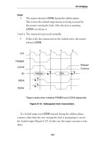
Figure 5-7 shows the clock waveform and the required measure-
ment points. Table 5-5 summarizes the specifications. For expansion
boards, clock measurements are made at the expansion board PCI
component and not at the connector. Note again the distinction
between the 5V and 3.3V signaling environments.
Electrical and Mechanical Issues
Table 5-5: Clock and reset specifications.
Figure 5-7: Clock waveform and required measurement points.
Symbol Parameter Min Max Units Notes
T
cyc
CLK Cycle Time 30 ∞ ns 1
T
high
CLK High Time 11 ns
T
low
CLK Low Time 11 ns
– CLK Slew Rate 1 4 V/ns 2
– RST# Slew Rate 50 – MV/ns 3
82
Notes for Table 5-5
1. In general, all PCI components must work with any clock frequency
between nominal DC and 33 MHz. Device operational parameters at
frequencies under 16 MHz may be guaranteed by design rather than
by testing. The clock frequency may be changed at any time during
the operation of the system so long as the clock edges remain “clean”
(monotonic) and the minimum cycle and high and low times are not
violated. For example, the use of spread spectrum techniques to reduce
EMI emissions is included in this requirement. The clock may only be
stopped in a low state. A variance on this specification is allowed for
components designed for use on the system motherboard only. These
components may operate at any single fixed frequency up to 33 MHz
and may enforce a policy of no frequency changes.
2. Rise and fall times are specified in terms of the edge rate measured in
V/ns. This slew rate must be met across the minimum peak-to-peak
portion of the clock waveform as shown in Figure 5-7.
3. The minimum RST# slew rate applies only to the rising (deassertion)
edge of the reset signal and ensures that system noise cannot render an
otherwise monotonic signal to appear to bounce in the switching range.
Timing Parameters
Table 5-6 lists the timing parameters for both the 5V and 3.3V
signaling environments.
Notes for Table 5-6
1. See the output timing measurement conditions in Figure 5-8.
2. For parts compliant to the 5V signaling environment:
Minimum times are evaluated with 0 pF equivalent load; maximum
times are evaluated with 50 pF equivalent load. Actual test capacitance
may vary, but results must be correlated to these specifications. Note that
faster buffers may exhibit some ring back when attached to a 50 pF lump
load which should be of no consequence as long as the output buffers are
in full compliance with slew rate and V/I curve specifications.
PCI Bus Demystified
83
Electrical and Mechanical Issues
Symbol Parameter Min Max Units Notes
t
val
CLK to Signal Valid Delay — 2 11 ns 1,2,3
bussed signals
T
val
(ptp) CLK to Signal Valid Delay — 2 12 ns 1,2,3
point to point
t
on
Float to Active Delay 2 ns 1,7
t
off
Active to Float Delay 28 ns 1,7
t
su
Input Setup Time to CLK — 7 ns 3,4,8
bussed signals
t
su
(ptp) Input Setup Time to CLK — 10, 12 ns 3,4
point to point
t
h
Input Hold Time from CLK 0ns4
T
rst
Reset active time after power stable 1 ms 5
T
rst-clk
Reset active time after CLK stable 100 µs5
T
rst-off
Reset active to output float delay 40 ns 5,6,7
T
rrsu
REQ64# to RST# Setup time 10*T
cyc
ns
T
rrh
RST# to REQ64# Hold time 0 50 ns
T
rhfa
RST# high to first configuration access 2
25
clocks
T
rhff
RST# high to first FRAME# assertion 5 clocks
Table 5-6: Timing parameters.
For parts compliant to the 3.3V signaling environment:
Minimum times are evaluated with same load used for slew rate
measurement (Figure 5-5); maximum times are evaluated with the load
circuits shown in Figure 5-9.
3. REQ# and GNT# are point-to-point signals and have different output
valid delay and input setup times than do bused signals. GNT# has a
setup of 10; REQ# has a setup of 12. All other signals are bused.
4. See the input timing measurement conditions in Figure 5-8.
5. CLK is stable when it meets the requirements in the previous section.
RST# is asserted and deasserted asynchronously with respect to CLK.
84
6. All output drivers must be asynchronously floated when RST# is active.
7. For purposes of Active/Float timing measurements, the Hi-Z or “off” state
is defined to be when the total current delivered through the component
pin is less than or equal to the leakage current specification.
8. Setup time applies only when the device is not driving the pin. Devices
cannot drive and receive signals at the same time.
PCI Bus Demystified
Figure 5-8: Input and output timing measurement conditions.
Symbol 5V Signaling 3.3V Signaling
V
th
2.4 0.6V
cc
V
tl
0.4 0.2V
cc
V
test
1.5 0.4V
cc
V
trise
N/a 0.285V
cc
V
tfall
N/a 0.615V
cc
V
max
2.0 0.4V
cc
Input Signal
Edge Rate
1 V/ns
Table 5-7: Measurement condition parameters.
Output timing measurements Input timing measurements
85
66 MHz PCI
66 MHz operation is defined in a way that allows 33 MHz cards
to coexist with 66 MHz cards in much the same way that 32-bit cards
coexist with 64-bit cards. 66 MHz is supported only in a 3.3 volt
signaling environment. A read-only bit in the Status Register of an
add-in card, 66MHZ_CAPABLE, identifies it as capable of 66 MHz
operation.
The M66EN pin was formerly defined as ground. It is pulled up
on a 66 MHz capable motherboard. 33 MHz cards will connect this
pin to the ground plane thus pulling it low to signify that the system
is limited to 33 MHz. So only if all cards are 66 MHz capable will the
system run at 66 MHz.
M66EN is an input to the clock generation circuit. If M66EN is
low, the clock reverts to 33 MHz.
Clock Specification
Table 5-8 shows the clock specifications for 66 MHz operation.
Not surprisingly, the numbers are roughly half the same values for
33 MHz operation as shown in Table 5-5.
Electrical and Mechanical Issues
Figure 5-9: Load circuits for 3.3V slew measurements.
86
Notes for Table 5-8
1. Refer to Figure 5-7 for details of clock waveform.
2. In general, all 66 MHz PCI components must work with any clock
frequency up to 66 MHz. CLK requirements vary depending upon
whether the clock frequency is above 33 MHz.
a. Device operational parameters at frequencies at or under
33 MHz will conform to the specifications in Table 5-5. The
clock frequency may be changed at any time during the operation
of the system so long as the clock edges remain “clean” (monotonic)
and the minimum cycle and high and low times are not violated.
The clock may only be stopped in a low state. A variance on this
specification is allowed for components designed for use on the
motherboard only.
b. For clock frequencies between 33 MHz and 66 MHz, the
clock frequency may not change except while RST# is asserted
or when spread spectrum clocking (SSC) is used to reduce EMI
emissions.
3. Rise and fall times are specified in terms of the edge rate measured in
V/ns. This slew rate must be met across the minimum peak-to-peak
portion of the clock waveform as shown in Figure 5-7.
4. The minimum clock period must not be violated for any single clock
cycle; i.e., accounting for all system jitter.
PCI Bus Demystified
Table 5-8: Clock specifications for 66 MHz operation.
Symbol Parameter Min Max Units Notes
T
cyc
CLK Cycle Time 15 30 ns 2,4
T
high
CLK High Time 6 ns
T
low
CLK Low Time 6 ns
– CLK Slew Rate 1.5 4 V/ns 3
87
Timing Parameters
Table 5-9 shows those timing parameters that change from 33 MHz
to 66 MHz.
Electrical and Mechanical Issues
Symbol Parameter Min Max Units Notes
t
val
CLK to Signal Valid
2 6 ns 1,2,3,5
Delay — bussed signals
T
val
(ptp)
CLK to Signal Valid
2 6 ns 1,2,3,5
Delay — point to point
t
on
Float to Active Delay 2 ns 1,5,7
t
off
Active to Float Delay 14 ns 1,7
t
su
Input Setup Time to CLK —
3 ns 3,4,7
bussed signals
t
su
(ptp)
Input Setup Time to CLK —
5 ns 3,4
point to point
Table 5-9: Timing parameters for 66 MHz operation.
Notes for Table 5-9
1. See the output timing measurement conditions in Figure 5-8.
2. Minimum times are evaluated with same load used for slew rate
measurement (Figure 5-5); maximum times are evaluated with the
load circuits shown in Figure 5-9.
3. REQ# and GNT# are point-to-point signals and have different output
valid delay and input setup times than do bused signals. GNT# and
REQ# have a setup time of 5 ns. All other signals are bused.
4. See the input timing measurement conditions in Figure 5-8.
5. When M66EN is asserted, the minimum specification for T
val
,
T
val
(ptp), and T
on
may be reduced to 1 ns if a mechanism is provided
to guarantee a minimum value of 2 ns when M66EN is deasserted.
88
6. For purposes of Active/Float timing measurements, the Hi-Z or
“off” state is defined to be when the total current delivered through
the component pin is less than or equal to the leakage current
specification.
7. Setup time applies only when the device is not driving the pin.
Devices cannot drive and receive signals at the same time.
Mechanical Details
Connector
PCI expansion cards utilize a connector derived from the
connector used by IBM’s Microchannel (see Figure 5-10). The
basic 32-bit bus uses a 124-pin connector where 4 pins are used
for a keyway that distinguishes 5 volt signaling from 3.3 volt
signaling. The same physical connector is used for both signaling
environments. In one orientation, the key accommodates 5V cards.
Rotated 180 degrees, it accommodates 3.3V cards.
PCI Bus Demystified
Figure 5-10: 32-bit PCI expansion card connector.
89
The 64-bit extension, built into the same connector molding,
extends the total number of pins to 184 as shown in Figure 5-11.
Note that the 64-bit connector requires two different implementations
to accommodate signaling environment keying.
Electrical and Mechanical Issues
Figure 5-11: 64-bit PCI expansion card connector.
Card
The basic PCI expansion card is designed to fit in standard
PC chassis available from any number of vendors. The card looks
essentially like an ISA or EISA card except that the components are
on the opposite side. This allows the implementation of shared slots
where a single chassis slot could accommodate either an ISA card
or a PCI card.
Because of the tight timing requirements imposed by operation
up to 66 MHz, the specification places limits on the trace length of
PCI signals on expansion boards. The 32-bit interface signals are
limited to 1.5" from the top edge of the connector to the PCI inter-
face device. The 64-bit extension signals are limited to 2". The CLK
signal must be 2.5" ± 0.1".
90
The specification also strongly recommends that the pinout of
the interface chip connecting to the PCI align exactly with the PCI
connector pinout as shown in Figure 5-12. This contributes to
shorter, more consistent stub lengths.
PCI Bus Demystified
Figure 5-12: Suggested pinout for PQFP PCI component.
Summary
PCI’s electrical characteristics are explicitly designed for low
power consumption. The bus does away with power-consuming
termination resistors and instead takes advantage of the wavefront
reflected from an unterminated bus line to minimize the drive
requirements of interface silicon. Because the specification is based
on CMOS, DC current requirements are almost nil and drivers must
be characterized in terms of a V/I curve during switching.
All PCI-shaped signals
below this line
91
PCI supports two signaling environments, 5 volts and 3.3 volts.
Again, the motivation is lower power consumption. Keying in the
expansion card connector prevents a card from being plugged into
the wrong signaling environment. There is provision for a universal
card that can work in either environment.
Like the 64-bit extension, the 66 MHz extension is implemented
in a way that allows 33 MHz cards to coexist with 66 MHz cards. The
CLK for a bus segment operates at 66 MHz only if all cards are 66 MHz
capable.
Electrical and Mechanical Issues
92
A key feature of PCI that distinguishes it from earlier busses
such as ISA is the ability to dynamically configure a system to avoid
resource conflicts. This is known as Plug and Play configurability or,
if you’re less optimistic, “Plug and Pray.”
Background
In the “old days,” configuration issues were generally handled
by jumpers on each add-in card. The jumpers would select operating
characteristics such as memory or I/O address space, interrupt vectors
and perhaps a DMA channel. Configuring such a card correctly
requires a fairly detailed knowledge of the system and its hardware.
Configure such a card wrong and it will likely conflict with
something else. This often leads to bizarre system behavior that is
difficult to diagnose.
In the PC world, various device types such as serial controllers,
video adapters and so on have a limited range of defined configura-
tions. Software drivers for these devices expect that the card will
be configured to one of the default settings. Information about the
device’s settings is typically conveyed by the command line that
starts the driver.
Plug and Play Configuration
C H A P T E R
6
93
In the world of Plug and Play, an add-in card tells the system
what it needs — how much memory or I/O space, does the device
require an interrupt and so on. Configuration software scans the
system at boot up time to determine total resource requirements and
then assigns resources like memory and I/O space and interrupts to
individual cards in a way that avoids resource conflicts.
The device driver can make no assumptions about a device’s
configuration. Instead, it must interrogate the device to determine
what resources have been allocated to it.
Configuration Address Space
PCI defines a third address space in addition to memory and I/O.
This is called configuration space and every logical function gets 256
bytes in this space. A function is selected for configuration space
access by asserting the corresponding device’s IDSEL signal together
with executing a Config Read or Config Write bus command.
Configuration Transactions
PCI-based systems require a mechanism that allows software to
generate transactions to Configuration space. This mechanism will
generally be located in the Host-to-PCI bridge. The specification
defines an appropriate mechanism for x86 processors. Other proces-
sors may, and probably will, use a similar approach.
The x86 configuration mechanism uses two DWORD read/write
registers in I/O space. These are:
CONFIG_ADDRESS 0x3f8
CONFIG_DATA 0x3fc
The layout of CONFIG_ADDRESS is shown in Figure 6-1. Bit 31
is an enable that determines when access to CONFIG_DATA is to be
Plug and Play Configuration
94
interpreted as a configuration transaction on the PCI bus. When bit
31 is 1, reads and writes to CONFIG_DATA are translated to PCI
configuration read and write cycles at the address specified by the
contents of CONFIG_ADDRESS. When bit 31 is 0, reads and
writes to CONFIG_DATA are simply passed through as PCI I/O
reads and writes. Bits 30 to 24 are reserved, read-only, and must
return 0 when read. Bits 23 to 16 identify a specific bus segment in
the system. Bits 15 to 11 select a device on that segment. Bits 10 to 8
select a function within the device (if the device supports multiple
functions). Bits 7 to 2 select a DWORD configuration register within
the function. Finally, bits 1 and 0 are reserved, read-only, and must
return 0 when read.
CONFIG_ADDRESS can only be accessed as a DWORD. Byte
or word accesses to CONFIG_ADDRESS are passed through to the
PCI bus.
PCI Bus Demystified
Figure 6-1: x86 configuration address.
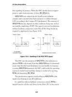
Driving IDSEL
A device is selected as the target of a configuration transaction by
asserting its IDSEL pin. The specification does not define the nature
of the mapping between the Device Number field and the individual
95
IDSEL signals. In the defined x86 configuration mechanism, the host
bridge decodes the Device Number field to drive one of the lines in
the range AD[31:11]. Every device then has its IDSEL pin connected
to exactly one of AD[31:11] as shown in Figure 6-2.
Plug and Play Configuration
Figure 6-2: Asserting IDSEL.
Configuration Header — Type 0
Of the 256 bytes of configuration space allocated to every func-
tion, the first 64 bytes are defined by the specification and are called
the Configuration Header. The remaining 192 bytes are available for
device-specific configuration functions. Figure 6-3 shows the layout
of the Configuration Header.
Header Type
Currently, three different header types are defined as indicated
by the value in byte 0xE (14 decimal). The Type 0 header is for
most devices. The Type 1 header describes a bridge device and the
Type 2 header describes a PC Card device. In all cases, the first three
DWORDS and the Header Type byte of the fourth DWORD are
the same.
96
The most significant bit of the Header Type is set to 1 if the
device is a multi-function device.
Identification Registers
Several fields in the header are read-only and serve to identify the
device along with various operational characteristics.
■ Vendor ID: Identifies the vendor of the device. More
specifically, it identifies the vendor of the PCI silicon.
PCI Bus Demystified
Figure 6-3: Type 0 configuration header.
97
Vendor ID codes are assigned by the PCI SIG.
■ Device ID: Identifies the device. This value is assigned by
the vendor.
■ Revision ID: Assigned by the device vendor to identify the
revision level of the device.
Two additional registers allow makers of PCI plug in adapters to
identify their devices.
■ Subsystem Vendor ID: Identifies the vendor of a functional
PCI device.
■ Subsystem Device ID: Assigned by the vendor to identify a
functional PCI device. Can also be used to identify indi-
vidual functions in a multi-function device.
The Class Code is a 24-bit read-only register that identifies the
basic function of the device. It is divided into three sections:
■ Base Class: Defines the basic functional category.
■ Sub-class: Identifies a device type or implementation
within the Base Class. For example, a mass storage con-
troller can be SCSI, IDE, floppy, etc. A network controller
can be Ethernet, token ring and so on.
■ Programming Interface: Defines specific register-level
implementations. For most classes this is simply 0, but it is
used for IDE controllers and other traditional PC peripher-
als.
Command Register
The read/writable Command Register provides coarse control
over a device’s ability to generate and respond to PCI cycles.
Plug and Play Configuration
98
Bit
0 When 1, allows the device to respond to PCI I/O space accesses.
1 When 1, allows the device to respond to PCI memory space accesses
2 When 1, enables the device to act as a bus master
3 When 1, allows a device to monitor Special Cycle operations.
4 When 1, a master is allowed to use the Memory Write and Invalidate
command if so capable. When 0, the master must use Memory Write
instead.
5 Controls how VGA devices handle access to VGA palette registers.
6 When 1, the device responds to a detected parity error by asserting
PERR#. If 0, the device ignores parity errors although it is still required
to generate parity.
7 Controls whether a device does address/data stepping. A device not
capable of stepping hardwires this bit to 0. A device that always steps
hardwires it to 1. A device that can do either must implement this bit
as writable.
PCI Bus Demystified
Figure 6-4: Configuration Command Register.
99
8 When 1, allows the device to assert SERR#.
9 When 1, allows a master to execute fast back-to-back transactions to
different targets. This bit will only be set if all targets are fast back-to-back
capable.
Note that writing all zeros to this register effectively disconnects
the device from the PCI bus for all accesses except configuration
cycles.
Status Register
The Status Register contains two types of information — Read
only bits that convey additional information about a device’s capa-
bilities and read/write bits that track bus related events.
Plug and Play Configuration
Figure 6-5: Configuration Status Register.
15 14 13 12 11 10 9 8 7 6 5 4 3
0
Reserved
Capabilities List
66 MHz Capable
Reserved
Fast Back-to-Back Capable
Data Parity Error Detected
DEVSEL timing
00 - fast
01 - medium
10 - slow
Signaled Target Abort
Received Target Abort
Received Master Abort
Signaled System Error
Detected Parity Error
100
The writable bits operate differently than normal. A bit is set to 1
by the occurrence of an event. Writing a 1 to a bit from the PCI bus
clears it. This simplifies programming. After reading the register and
determining that error bits are set, you simply write the same value
back to clear them.
Bit
4 RO. 1 = Extended capabilities pointer exists.
5 RO. 1 = device is capable of 66 MHz operation.
6 RO. 1 = device supports “user definable features”.
7 RO. 1 = target device supports fast back-to-back transactions to different
targets.
8 RW. Only implemented by masters. Set if
■ The agent asserted PERR# itself or observed PERR# asserted
■ The agent was the bus master for the operation in which the error
occurred AND
■ Its Parity Error Response bit is set
9–10 RO. DEVSEL# timing
00 = Fast
01 = medium
10 = slow
11 = reserved
11 RW. Set by a target when it terminates a transaction with Target Abort
12 RW. Set by a master when its transaction is terminated by Target Abort
13 RW. Set by a master when it terminates a transaction with Master
Abort
14 RW. Set by a device that asserts SERR#
15 RW. Set by a device whenever it detects a parity error, even if parity
error handling is disabled.
PCI Bus Demystified
101
Built-in Self-Test Register (BIST)
This optional mechanism provides a standardized way of imple-
menting self-test on plug-in cards. Devices that don’t support BIST
must return a value of 0 when this register is read.
Plug and Play Configuration
Figure 6-6: Built-in self-test (BIST) register.
Bit
7 RO. 1 = device supports BIST
6 RW. Write 1 to invoke BIST. Device resets bit when BIST is complete.
5–4 Reserved. Read as 0.
3–0 Completion code. 0 = device has passed test. Non-zero value indicates
failure. Failure codes are device specific.
Latency Timer
The Latency Timer is required and must be a read/writable register
for any master capable of bursting more than two data phases. The
value written here is the minimum number of clock cycles that the
7 6 5 4 3 2 1 0
Completion Code
0 = BIST succeeded
Reserved
Write 1 to start BIST
Device resets when BIST
complete
1 = device supports BIST
(read only)