the PCI Bus demystified phần 4 docx
Bạn đang xem bản rút gọn của tài liệu. Xem và tải ngay bản đầy đủ của tài liệu tại đây (350.04 KB, 21 trang )
59
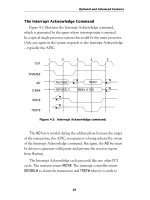
The Interrupt Acknowledge Command
Figure 4-2 illustrates the Interrupt Acknowledge command,
which is generated by the agent whose interrupt input is asserted.
In a typical single processor system this would be the main processor.
Only one agent in the system responds to the Interrupt Acknowledge
— typically the APIC.
Optional and Advanced Features
Figure 4-2: Interrupt Acknowledge command.
The AD bus is invalid during the address phase because the target
of the transaction, the APIC, recognizes it is being selected by virtue
of the Interrupt Acknowledge command. But again, the AD bus must
be driven to generate valid parity and prevent the receiver inputs
from floating.
The Interrupt Acknowledge cycle proceeds like any other PCI
cycle. The initiator asserts IRDY#. The interrupt controller asserts
DEVSEL# to claim the transaction and TRDY# when it is ready to
Not Valid
INT-ACK
IRDY#
BE#’s (1110)
CLK
FRAME#
AD
C/BE#
TRDY#
5
1
23
4
Vector
60
supply the interrupt vector. The C/BE# bus indicates which bytes of
the interrupt vector are valid. Because PCI is processor independent,
we don’t necessarily know the nature or size of an interrupt vector.
That’s a function of the host processor architecture. The example
shows a typical x86 system where the interrupt vector is a single byte.
“Special” Cycle
The Special Cycle provides a mechanism to broadcast informa-
tion simultaneously to multiple targets. The specification suggests
that it is a useful way to convey sideband information to one or
more devices without the need for additional wires on the backplane.
One use for this facility is to broadcast processor status such as Halt
and Shutdown.
By definition, a Special Cycle is not directed at a specific target
but rather to any and all targets that have an interest in the message
being broadcast. This has several consequences:
■ The AD bus is not valid during the address phase. Of
course it must still be driven in order to generate parity
correctly.
■ Targets do not assert DEVSEL# or TRDY#.
■ Since DEVSEL# is not asserted, the only way for the
transaction to terminate is with a Master Abort.
During the data phase AD[15:0] conveys a predefined message
type. AD[31:16] may optionally carry message-dependent data.
Table 4-2 shows the currently defined messages.
Figure 4-3 shows the timing of a Special Cycle.
PCI Bus Demystified
61
Optional and Advanced Features
Table 4-2
Message Code Message
(AD[15:0]) Type
0x0000 Shutdown. Processor is entering a shut-down
mode, probably due to an unrecoverable
software problem.
0x0001 Halt. Processor has executed a halt instruction.
0x0002 X86-specific message. AD[31:16] contains an
Intel-specific message.
0x0003 Reserved. Assigned by PCI SIG steering
to 0xfff committee.
Figure 4-3: Timing diagram of a Special Cycle.
62
Clock
2 Master asserts FRAME#. AD is not valid, C/BE# = Special
Cycle.
3 Master places message on AD, asserts IRDY# and deasserts
FRAME#. All targets must latch the message on the first
clock in which IRDY# is asserted.
4 – 7 Master waits to time out with a Master Abort.
A Special Cycle is always a full DWORD transfer so all four
C/BE# lines are asserted during the data phase.
Because of the Master Abort requirement, a Special Cycle is a
minimum of six clock cycles (more if the master delays the assertion
of IRDY#).
Multiple data phases are permitted but at present there are no
messages that would require more than one data phase. The require-
ment that data be latched on the first clock following the assertion
of IRDY# implies that IRDY# must be deasserted for at least one clock
before executing a second, or subsequent, data phase.
64-bit Extensions
The PCI specification defines an optional extension to 64 bits
for memory targets in a way that allows 64-bit agents to seamlessly
inter-operate with 32-bit agents. 64-bit transfers only occur if both
the initiator and target support 64 bits. Otherwise, transfers default
to 32 bits. The “negotiation” to transfer 64 bits occurs on a per-
transaction basis and is facilitated by two optional signals; REQ64#
and ACK64#.
PCI Bus Demystified
63
64-bit Bus
Figure 4-4 shows a 64-bit transaction. A 64-bit master asserts
REQ64# at the same time as FRAME# in clock 2. In this case the
selected target also supports 64-bit transfers so it asserts ACK64#
together with DEVSEL# in clock 3. This example shows a read trans-
action. The target places the low-order 32 bits on AD[31:0] and the
high-order on AD[63:32]. The master places byte enable information
for AD[63:32] on C/BE#[7:4]. Parity for AD[63:32] and C/BE#[7:4]
is computed and checked on PAR64.
Optional and Advanced Features
Figure 4-4: Timing diagram of a 64-bit transaction.
64
Figure 4-5 shows what happens when a 64-bit master executes a
write transaction to a 32-bit target. In clock 2 the master asserts
REQ64# as before. In clock 3 the master places up to eight bytes of
data on AD[63:0] and corresponding byte enables on C/BE#[7:0].
At the same time the master detects DEVSEL# asserted with ACK64#
not asserted indicating that the target only supports 32 bits. In clock
4 the master moves the upper four bytes (Data-2) down to AD[31:0].
A 64-bit target communicating with a 32-bit master knows that it
must revert to 32 bits because it detects REQ64# unasserted.
PCI Bus Demystified
Figure 4-5: Execution of a write transaction
from a 64-bit master to a 32-bit target.
65
64-bit Addressing — The Dual Address Cycle
There is another optional mechanism that permits 32-bit agents
to address memory locations above 4 GBytes. This is accomplished
by adding a second address phase to a transaction in the form of a
Dual Address Cycle command (DAC). Note that even if a target
supports DAC, standard single address commands (SAC) must be
used for locations below 4 GBytes. 64-bit addressing is only supported
in the memory space.
Figure 4-6 illustrates the Dual Address Command. In clock 2,
the master issues the DAC command on C/BE#[3:0] and puts the
low-order address on AD[31:0]. A 64-bit master puts the high-order
address on AD[63:32] and the transaction command (in this case
Mem Read) on C/BE[7:4]. In clock 3 the master places the high-
order address on AD[31:0] and the normal transaction command on
C/BE#[3:0].
Optional and Advanced Features
Figure 4-6: Dual Address Command used in 64-bit addressing.
66
A 64-bit target can decode the entire address and transaction
command during the first address phase. However, the master must
still execute the DAC because it won’t know until the target is
selected that the target is 64-bit capable. But by decoding the address
and command in the first address phase, a medium or slow DEVSEL
target saves one clock cycle.
The DAC command is always exactly one clock cycle. Conse-
quently, address stepping is not permitted for the DAC command.
Summary
The topics covered in this chapter, interrupts, the Special Cycle
command and 64-bit extensions, are all optional features of PCI.
The specification provides for four interrupt signals from each
PCI device. A single function device may only use one of the inter-
rupt signals, INTA#. Multi function devices may use any combination
of the four. The routing of the four signals among the devices in a
system is at the discretion of the designer. Interrupts are defined as
assertion low, level-sensitive and asynchronous to the clock.
The Special Cycle command is a broadcast mechanism that
may, in certain cases, substitute for sideband signals. Special Cycles
are not directed at a specific target and so no target responds. The
Special Cycle is always terminated by a Master Abort.
The PCI bus may be extended to 64 bits in a way that allows
32-bit agents to interoperate with 64-bit agents. The Dual Address
command (DAC) provides a way for 32-bit agents to access a 64-bit
memory address space.
PCI Bus Demystified
67
This chapter summarizes the electrical signaling environment of
PCI and mechanical issues related to add-in cards. The objective is to
highlight the electrical features of PCI without getting bogged down
in details that are primarily of interest to integrated circuit designers.
To dig deeper, refer to the current revision of the PCI specification.
A “Green” Architecture
Many aspects of PCI’s electrical specification are explicitly
intended to reduce power consumption. Not only is this environ-
mentally correct, it is essential for mobile and portable devices. PCI
is based on CMOS, which means that steady state DC currents are
minimal and in fact most DC drive current goes to pull-up resistors.
The bus protocol assures that bus receivers are not allowed to float
such that they might oscillate and consume unnecessary power.
Finally, the most interesting aspect of low power consumption is that
PCI is based on “reflected wave” switching rather than the more
traditional “incident wave” switching.
Incident Wave Switching — the Old Way
Traditional bus architectures have stressed the need for proper
termination of all bus lines to prevent unwanted reflections. Every
Electrical and
Mechanical Issues
C H A P T E R
5
68
signal on a backplane bus is really a transmission line with a charac-
teristic impedance of about 120 ohms. If the ends are not terminated,
a pulse travelling down the line will be reflected back from the end
possibly causing unwanted interference.
The solution is to terminate both ends of the bus in the character-
istic impedance. Figure 5-1 shows a typical termination arrangement.
The “Thevenin equivalent” impedance of the 180/330 ohm divider
is 120 ohms while the divider maintains an open-circuit voltage of
3.4 volts.
PCI Bus Demystified
Figure 5-1: “Traditional bus” — incident wave switching.
This “incident wave” approach is fundamentally incompatible
with the objective of low power consumption. Each of the divider
networks in this example consumes 10 ma, or 20 ma per signal line.
For the 46 bussed signals of the PCI, that’s almost an amp. At 5 volts,
that’s about 5 watts just for the termination resistors!
Each driver must be capable of sinking 50 ma when it drives the
line to the low voltage state. Such high power drivers require a lot
of silicon real estate and dissipate substantial power themselves.
Vcc
Vcc
Driver Receiver
From/To
Functional
Logic
180 ohms
330 ohms
3.4 volts
Characteristic
Impedance 120 ohms
10 ma
25 ma
25 ma
69
Electrical and Mechanical Issues
The current surges resulting from many drivers switching on
or off at once can cause large noise spikes on the power lines, not to
mention crosstalk between bus signals.
Reflected Wave Switching — the New Way
Not surprisingly then, PCI takes a radically different approach to
bus termination. It eliminates the termination networks altogether
and actually takes advantage of the reflected wave front. As shown in
Figure 5-2, a PCI bus driver is designed to drive the line about “half
way”, and only half way. As the wave front propagates to the end of
the line, it is insufficient to switch the receivers that it passes. When
the wave front reaches the end of the bus, it is reflected back doubled
in magnitude. So the receivers switch as the wave front passes them
the second time going in the other direction.
Figure 5-2: Reflected wave switching.
Reflected wave switching requires twice the propagation time of
incident wave switching. It also requires much more careful attention
to trace length and layout. The specification limits propagation time
to 10 ns at 33 MHz and, as we’ll see shortly, sets very specific limits
on trace length.
1.5 volts
3 volts
70
Preventing Receiver Inputs from Floating
If a tri-state bus line is not driven, i.e. it is tri-stated, and it is
not terminated with a pull-up resistor, it is said to be “floating”.
The voltage level of a floating bus line tends to settle around the
switching point of the bus receivers. This may cause the receiver to
oscillate and consume more power than it should. There are basically
two approaches to preventing a bus line from floating:
1. Always drive the line, or
2. Pull it up to the signaling voltage (3.3V or 5V) through
a resistor
The PCI spec requires that AD[31::0], PAR and C/BE[3::0] be
driven to stable states when the bus is idle. If the bus is parked,
the agent on which it is parked should drive AD and C/BE. If the bus
is not parked then the central resource should drive AD and C/BE.
AD[63::32], PAR64 and C/BE[7:4] require pull up resistors because
otherwise they would float when a 32-bit agent is driving the bus.
The control signals all require pull ups since they can’t be driven
while the bus is idle. This includes FRAME#, DEVSEL#, IRDY#,
TRDY#, STOP#, SERR#, PERR#, LOCK#, REQ64#, ACK64# and the
INTx# signals. Typical resistor values are 2.7 kilohm in the 5V signal-
ing environment and 8.2 kilohm in the 3V signaling environment.
Signaling Environments — 3.3V and 5V
At the present time most computer busses use 5 volt TTL-
compatible signaling levels. There is, however, a trend toward
3.3 volt logic, particularly in portable and mobile environments
where power consumption must be minimized. Unfortunately, these
two logic families don’t mix well together, so PCI has developed
PCI Bus Demystified
71
separate electrical specifications for each signaling environment.
When we speak of a “signaling environment,” we are referring to the
signal level on the PCI pins and not to the voltage that powers the
board.
The motherboard (including connectors) defines the signaling
environment for the bus, whether it be 5V or 3.3V. A 5V expansion
board is designed to work only in a 5V signaling environment.
Similarly, a 3.3V board works only in a 3.3V signaling environment.
To prevent boards from being installed incorrectly, the connector has
different keying for the two signaling environments (see Figure 5-3).
There is also a provision for a “universal board”, one that can
operate in either signaling environment. A universal board has
notches for both signaling keys. There are three pins on the con-
nector labeled Vio. A universal board powers its PCI transceivers
from the Vio pins. The motherboard connects the Vio pins to the
power rail corresponding to system’s signaling environment.
Electrical and Mechanical Issues
Figure 5-3: 3.3V vs. 5V keying.
“5 volt” connector “3.3 volt” connector
“5 volt” Board “3.3 volt” Board
Dual Voltage Board
72
PCI defines four power rails: +5V, +3.3V, +12V and –12V.
Systems implementing the 3.3V signaling environment are required
to provide all four supplies. Systems with 5V signaling are not
required to provide 3.3V but it is strongly “encouraged.”
Many of the figures, tables and their accompanying notes in the
remainder of this chapter have been taken from Rev. 2.2 of the PCI
Specification. As always, refer to the specification for more details.
5 Volt Signaling Environment
The 5 volt specifications are given in terms of absolute voltages
based on standard TTL levels.
DC Specifications
Table 5-1 summarizes the 5 volt DC specifications.
Notes for Table 5-1
1. Input leakage currents include hi-Z output leakage for all bi-directional
buffers with tri-state outputs.
2. Signals without pull-up resistors must have 3 ma low output current.
Signals requiring pull up must have 5 ma; the latter include, FRAME#,
TRDY#, IRDY#, DEVSEL#, STOP#, SERR#, PERR#, LOCK#, and, when
used, AD[63::32], C/BE[7::4]#, PAR64, REQ64#, and ACK64#.
3. Absolute maximum pin capacitance for a PCI input is 10 pF (except
for CLK) with an exception granted to motherboard-only devices,
which could be up to 16 pF, in order to accommodate PGA packaging.
This would mean, in general, that components for expansion boards
would need to use alternatives to ceramic PGA packaging (i.e., PQFP,
SGA, etc.).
4. Lower capacitance on this input-only pin allows for non-resistive
coupling to AD[xx].
PCI Bus Demystified
73
5. This is a recommendation, not an absolute requirement. The actual
value should be provided with the component data sheet.
6. This input leakage is the maximum allowable leakage in the PME#
open drain driver when power is removed from V
cc
of the component.
This assumes that no event has occurred to cause the device to attempt
to assert PME#.
Electrical and Mechanical Issues
Symbol Parameter Condition Min Max Units Notes
V
cc
Supply Voltage 4.75 5.25 V
V
ih
Input High Voltage 2.0 V
cc
+0.5 V
V
il
Input Low Voltage –0.5 0.8 V
I
ih
Input High
V
in
= 2.7 70 µA1
Leakage Current
I
il
Input Low
V
in
= 0.5 –70 µA1
Leakage Current
V
oh
Output High
I
out
= –2 ma 2.4 V
Voltage
V
ol
Output Low
I
out
= 3 ma, 6 ma 0.55 V 2
Voltage
C
in
Input Pin
10 pF 3
Capacitance
C
clk
CLK Pin
512pF
Capacitance
C
IDSEL
IDSEL Pin
8pF4
Capacitance
L
pin
Pin Inductance 20 nH 5
I
Off
PME# Input V
o
≤ 5.25 V
1 µA6
V
cc
off or floating
Table 5-1: DC specifications for 5V signaling.
Leakage
74
AC Specifications
For the reflected wave switching mechanism to work properly,
the output driver must source or sink enough instantaneous current
to develop the initial half amplitude voltage step on a bus wire loaded
with PCI components. But it must not source or sink too much current
such that it drives the line too far possibly resulting in undesirable
reflections. Table 5-2 summarizes the AC specifications for the 5 volt
signaling environment while Figure 5-4 shows the V/I curves that
characterize a PCI driver. These numbers are based on a maximum
of ten AC loads where each expansion board connector is considered
one AC load. Typical configurations are six motherboard loads plus
two expansion connectors or two motherboard loads and four expan-
sion connectors.
Notes for Table 5-2
1. Refer to the V/I curves in Figure 5-4. Switching current characteristics
for REQ# and GNT# are permitted to be one half of that specified
here; i.e., half size output drivers may be used on these signals. This
specification does not apply to CLK and RST# which are system outputs.
“Switching Current High” specifications are not relevant to SERR#,
PME#, INTA#, INTB#, INTC#, and INTD# which are open drain outputs.
2. Note that this segment of the minimum current curve is drawn from
the AC drive point directly to the DC drive point rather than toward
the voltage rail (as is done in the pull-down curve). This difference is
intended to allow for an optional N-channel pull-up.
3. Maximum current requirements must be met as drivers pull beyond
the first step voltage. Equations defining these maximums (A and B)
are provided with the respective diagrams in Figure 5-4. The equation
defined maxima should be met by design. In order to facilitate
component testing, a maximum current test point is defined for each
side of the output driver.
PCI Bus Demystified
75
Electrical and Mechanical Issues
Table 5-2: AC specifications for 5V signaling.
Symbol Parameter Condition Min Max Units Notes
I
oh(AC
) Switching 0 < V
out
≤ 1.4 –44 mA 1
1.4 < V
out
< 2.4
–44+( V
out
–1.4)
mA 1,2
3.1 < V
out
< V
cc
Eq. A 1,3
(Test Point) V
out
= 3.1 –142 mA 3
I
ol(AC
) Switching V
out
≥ 2.2 95 mA 1
2.2 > V
out
> 0.55
V
out
mA 1
0.71 > V
out
> 0 Eq. B 1,3
(Test Point) V
out
= 0.71 206 mA 3
I
cl
Low Clamp
–5 < V
in
≤ –1
–25+( V
in
+1)
mA
Current
slew
r
Output Rise
0.4V to 2.4V load 1 5 V/ns 4
Slew Rate
slew
f
Output Fall
2.4V to 0.4V load 1 5 V/ns 4
Slew Rate
0.015
0.024
Current High
0.023
Current Low
4. This parameter is to be interpreted as the cumulative edge rate across the
specified range, rather than the instantaneous rate at any point within the
transition range. The specified load (Figure 5-5) is optional; i.e., the designer
may elect to meet this parameter with an unloaded output per revision 2.0 of
the PCI Local Bus Specification. However, adherence to both maximum and
minimum parameters is now required (the maximum is no longer simply a
guideline). Since adherence to the maximum slew rate was not required prior
to revision 2.1 of the specification, there may be components in the market for
some time that have faster edge rates; therefore, motherboard designers must
bear in mind that rise and fall times faster than this specification could occur,
and should ensure that signal integrity modeling accounts for this. Rise slew
rate does not apply to open drain outputs.
76
PCI Bus Demystified
Figure 5-4: Characteristic V/I curves for a PCI driver in
the 5V signaling environment.
Figure 5-5: Specified load for output rise and fall
slew rate measurements.
output
buffer
1/2 inch max.
pin
Vcc
10 pF
1K Ω 1K Ω
77
3.3 Volt Signaling Environment
The 3.3 volt environment is based on V
cc
-relative switching
voltages and is optimized for CMOS. The intent is that components
connect directly together, whether on the motherboard or an expan-
sion board, without any external buffers or other “glue.”
DC Specifications
Table 5-3 summarizes the DC specifications for the 3.3 volt envi-
ronment.
Electrical and Mechanical Issues
Table 5-3: DC specifications for 3.3V signaling.
Symbol Parameter Condition Min Max Units Notes
V
cc
Supply Voltage 3.0 3.6 V
V
ih
Input High Voltage 0.5V
cc
V
cc
+0.5 V
V
il
Input Low Voltage –0.5 0.3V
cc
V
V
ipu
Input Pull-up
0.7V
cc
V1
Voltage
I
il
Input Leakage
0 < V
in
< V
cc
±10 µA2
Current
V
oh
Output High
I
out
= –500 µA 0.9V
cc
V
Voltage
V
ol
Output Low
I
out
= 1500 µA 0.1V
cc
V
Voltage
C
in
Input Pin
10 pF 3
Capacitance
C
clk
CLK Pin
512pF
Capacitance
C
IDSEL
IDSEL Pin
8pF4
Capacitance
L
pin
Pin Inductance 20 nH 5
I
Off
PME# input
V
o
≤ 3.6 V
1 µA6
leakage
V
cc
off or floating
78
Notes for Table 5-3
1. This specification should be guaranteed by design. It is the minimum
voltage to which pull-up resistors are calculated to pull a floated
network. Applications sensitive to static power utilization must assure
that the input buffer is conducting minimum current at this input
voltage.
2. Input leakage currents include hi-Z output leakage for all bi-directional
buffers with tri-state outputs.
3. Absolute maximum pin capacitance for a PCI input is 10 pF (except
for CLK) with an exception granted to motherboard-only devices,
which could be up to 16 pF, in order to accommodate PGA packaging.
This would mean, in general, that components for expansion boards
would need to use alternatives to ceramic PGA packaging (i.e., PQFP,
SGA, etc.).
4. Lower capacitance on this input-only pin allows for non-resistive
coupling to AD[xx].
5. This is a recommendation, not an absolute requirement. The actual
value should be provided with the component data sheet.
6. This input leakage is the maximum allowable leakage in the PME#
open drain driver when power is removed from V
cc
of the component.
This assumes that no event has occurred to cause the device to attempt
to assert PME#.
AC Specifications
Table 5-4 summarizes the AC specifications for the 3.3 volt
signaling environment while Figure 5-6 illustrates the corresponding
V/I curves.
Notes for Table 5-4
1. Refer to the V/I curves in Figure 5-6. Switching current characteristics
for REQ# and GNT# are permitted to be one half of that specified here;
i.e., half size output drivers may be used on these signals. This specifi-
PCI Bus Demystified
79
cation does not apply to CLK and RST# which are system outputs.
“Switching Current High” specifications are not relevant to SERR#,
PME#, INTA#, INTB#, INTC#, and INTD# which are open drain outputs.
2. Maximum current requirements must be met as drivers pull beyond
the first step voltage. Equations defining these maximums (C and D)
are provided with the respective diagrams in Figure 5-6. The equation
defined maxima should be met by design. In order to facilitate compo-
nent testing, a maximum current test point is defined for each side of
the output driver.
Electrical and Mechanical Issues
Table 5-4: AC specifications for 3.3V signaling.
Current High
Symbol Parameter Condition Min Max Units Notes
I
oh(AC
) Switching 0 < V
out
≤ 0.3V
cc
–12 V
cc
mA 1
0.3V
cc
<V
out
<0.9V
cc
–17.1(V
cc
– V
out
)mA1
0.7V
cc
< V
out
< V
cc
Eq. C 1,2
(Test Point) V
out
= 0.7V
cc
–32V
cc
mA 2
I
ol(AC
) Switching V
cc
> V
out
≥ 0.6V
cc
16V
cc
mA 1
0.6V
cc
>V
out
> 0.1V
cc
26.7V
out
mA 1
0.18V
cc
> V
out
> 0 Eq. D 1,2
(Test Point) V
out
= 0.18V
cc
38V
cc
mA 2
I
cl
Low Clamp
–3 < V
in
≤ –1
–25+( V
in
+1)
mA
Current
I
ch
High Clamp
V
cc
+4 > V
in
≥ V
cc
+1
25+( V
in
–V
cc
–1)
mA
Current
slew
r
Output Rise
0.2V
cc
to 0.6V
cc
load 1 4 V/ns 3
Slew Rate
slew
f
Output Fall
0.6V
cc
to 0.2V
cc
load 1 4 V/ns 3
Slew Rate
Current Low
0.015
0.015