Bộ điều chỉnh chuyển mạch nguồn Switching regulators
Bạn đang xem bản rút gọn của tài liệu. Xem và tải ngay bản đầy đủ của tài liệu tại đây (485.1 KB, 71 trang )
SWITCHING REGULATORS
3.1
SECTION 3
SWITCHING REGULATORS
Walt Kester, Brian Erisman
INTRODUCTION
Virtually all of today's electronic systems require some form of power conversion.
The trend toward lower power, portable equipment has driven the technology and
the requirement for converting power efficiently. Switchmode power converters,
often referred to simply as "switchers", offer a versatile way of achieving this goal.
Modern IC switching regulators are small, flexible, and allow either step-up (boost)
or step-down (buck) operation.
When switcher functions are integrated and include a switch which is part of the
basic power converter topology, these ICs are called “switching regulators”. When no
switches are included in the IC, but the signal for driving an external switch is
provided, it is called a “switching regulator controller”. Sometimes - usually for
higher power levels - the control is not entirely integrated, but other functions to
enhance the flexibility of the IC are included instead. In this case the device might
be called a “controller” of sorts - perhaps a “feedback controller” if it just generates
the feedback signal to the switch modulator. It is important to know what you are
getting in your controller, and to know if your switching regulator is really a
regulator or is it just the controller function.
Also, like switchmode power conversion, linear power conversion and charge pump
technology offer both regulators and controllers. So within the field of power
conversion, the terms “regulator” and “controller” can have wide meaning.
The most basic switcher topologies require only one transistor which is essentially
used as a switch, one diode, one inductor, a capacitor across the output, and for
practical but not fundamental reasons, another one across the input. A practical
converter, however, requires several additional elements, such as a voltage
reference, error amplifier, comparator, oscillator, and switch driver, and may also
include optional features like current limiting and shutdown capability. Depending
on the power level, modern IC switching regulators may integrate the entire
converter except for the main magnetic element(s) (usually a single inductor) and
the input/output capacitors. Often, a diode, the one which is an essential element of
basic switcher topologies, cannot be integrated either. In any case, the complete
power conversion for a switcher cannot be as integrated as a linear regulator, for
example. The requirement of a magnetic element means that system designers are
not inclined to think of switching regulators as simply “drop in” solutions. This
presents the challenge to switching regulator manufacturers to provide careful
design guidelines, commonly-used application circuits, and plenty of design
assistance and product support. As the power levels increase, ICs tend to grow in
complexity because it becomes more critical to optimize the control flexibility and
precision. Also, since the switches begin to dominate the size of the die, it becomes
more cost effective to remove them and integrate only the controller.
SWITCHING REGULATORS
3.2
The primary limitations of switching regulators as compared to linear regulators are
their output noise, EMI/RFI emissions, and the proper selection of external support
components. Although switching regulators do not necessarily require transformers,
they do use inductors, and magnetic theory is not generally well understood.
However, manufacturers of switching regulators generally offer applications support
in this area by offering complete data sheets with recommended parts lists for the
external inductor as well as capacitors and switching elements.
One unique advantage of switching regulators lies in their ability to convert a given
supply voltage with a known voltage range to virtually any given desired output
voltage, with no “first order” limitations on efficiency. This is true regardless of
whether the output voltage is higher or lower than the input voltage - the same or
the opposite polarity. Consider the basic components of a switcher, as stated above.
The inductor and capacitor are, ideally, reactive elements which dissipate no power.
The transistor is effectively, ideally, a switch in that it is either “on”, thus having no
voltage dropped across it while current flows through it, or “off”, thus having no
current flowing through it while there is voltage across it. Since either voltage or
current are always zero, the power dissipation is zero, thus, ideally, the switch
dissipates no power. Finally, there is the diode, which has a finite voltage drop while
current flows through it, and thus dissipates some power. But even that can be
substituted with a synchronized switch, called a “synchronous rectifier”, so that it
ideally dissipates no power either.
Switchers also offer the advantage that, since they inherently require a magnetic
element, it is often a simple matter to “tap” an extra winding onto that element and,
often with just a diode and capacitor, generate a reasonably well regulated
additional output. If more outputs are needed, more such taps can be used. Since the
tap winding requires no electrical connection, it can be isolated from other circuitry,
or made to “float” atop other voltages.
Of course, nothing is ideal, and everything has a price. Inductors have resistance,
and their magnetic cores are not ideal either, so they dissipate power. Capacitors
have resistance, and as current flows in and out of them, they dissipate power, too.
Transistors, bipolar or field-effect, are not ideal switches, and have a voltage drop
when they are turned on, plus they cannot be switched instantly, and thus dissipate
power while they are turning on or off.
As we shall soon see, switchers create ripple currents in their input and output
capacitors. Those ripple currents create voltage ripple and noise on the converter’s
input and output due to the resistance, inductance, and finite capacitance of the
capacitors used. That is the conducted part of the noise. Then there are often ringing
voltages in the converter, parasitic inductances in components and PCB traces, and
an inductor which creates a magnetic field which it cannot perfectly contain within
its core - all contributors to radiated noise. Noise is an inherent by-product of a
switcher and must be controlled by proper component selection, PCB layout, and, if
that is not sufficient, additional input or output filtering or shielding.
SWITCHING REGULATORS
3.3
INTEGRATED CIRCUIT SWITCHING REGULATORS
n Advantages:
u High Efficiency
u Small
u
Flexible - Step-Up (Boost), Step-Down (Buck), etc.
n Disadvantages
u Noisy (EMI, RFI, Peak-to-Peak Ripple)
u Require External Components (L’s, C’s)
u Designs Can Be Tricky
u Higher Total Cost Than Linear Regulators
n "Regulators" vs. "Controllers"
Figure 3.1
Though switchers can be designed to accommodate a range of input/output
conditions, it is generally more costly in non-isolated systems to accommodate a
requirement for both voltage step-up and step-down. So generally it is preferable to
limit the input/output ranges such that one or the other case can exist, but not both,
and then a simpler converter design can be chosen.
The concerns of minimizing power dissipation and noise as well as the design
complexity and power converter versatility set forth the limitations and challenges
for designing switchers, whether with regulators or controllers.
The ideal switching regulator shown in Figure 3.2 performs a voltage conversion and
input/output energy transfer without loss of power by the use of purely reactive
components. Although an actual switching regulator does have internal losses,
efficiencies can be quite high, generally greater than 80 to 90%. Conservation of
energy applies, so the input power equals the output power. This says that in step-
down (buck) designs, the input current is lower than the output current. On the
other hand, in step-up (boost) designs, the input current is greater than the output
current. Input currents can therefore be quite high in boost applications, and this
should be kept in mind, especially when generating high output voltages from
batteries.
SWITCHING REGULATORS
3.4
THE IDEAL SWITCHING REGULATOR
n P
in
= P
out
n Efficiency = P
out
/ P
in
= 100%
n v
in
• i
in
= v
out
• i
out
n
n Energy Must be Conserved!
v
out
v
in
i
in
i
out
==
LOSSLESS
SWITCHING
REGULATOR
i
in
i
out
LOAD
v
in
v
out
P
in
P
out
+
Figure 3.2
Design engineers unfamiliar with IC switching regulators are sometimes confused
by what exactly these devices can do for them. Figure 3.3 summarizes what to
expect from a typical IC switching regulator. It should be emphasized that these are
typical specifications, and can vary widely, but serve to illustrate some general
characteristics.
Input voltages may range from 0.8 to beyond 30V, depending on the breakdown
voltage of the IC process. Most regulators are available in several output voltage
options, 12V, 5V, 3.3V, and 3V are the most common, and some regulators allow the
output voltage to be set using external resistors. Output current varies widely, but
regulators with internal switches have inherent current handling limitations that
controllers (with external switches) do not. Output line and load regulation is
typically about 50mV. The output ripple voltage is highly dependent upon the
external output capacitor, but with care, can be limited to between 20mV and
100mV peak-to-peak. This ripple is at the switching frequency, which can range
from 20kHz to 1MHz. There are also high frequency components in the output
current of a switching regulator, but these can be minimized with proper external
filtering, layout, and grounding. Efficiency can also vary widely, with up to 95%
sometimes being achievable.
SWITCHING REGULATORS
3.5
WHAT TO EXPECT FROM A SWITCHING REGULATOR IC
n Input Voltage Range: 0.8V to 30V
n Output Voltage:
u “Standard”: 12V, 5V, 3.3V, 3V
u “Specialized”: VID Programmable for Microprocessors
u (Some are Adjustable)
n
Output Current
u Up to 1.5A, Using Internal Switches of a Regulator
u No Inherent Limitations Using External Switches with a
Controller
n Output Line / Load Regulation: 50mV, typical
n Output Voltage Ripple (peak-peak) :
20mV - 100mV @ Switching Frequency
n Switching Frequency: 20kHz - 1MHz
n Efficiency: Up to 95%
Figure 3.3
POPULAR APPLICATIONS OF SWITCHING REGULATORS
For equipment which is powered by an AC source, the conversion from AC to DC is
generally accomplished with a switcher, except for low-power applications where size
and efficiency concerns are outweighed by cost. Then the power conversion may be
done with just an AC transformer, some diodes, a capacitor, and a linear regulator.
The size issue quickly brings switchers back into the picture as the preferable
conversion method as power levels rise up to 10 watts and beyond. Off-line power
conversion is heavily dominated by switchers in most modern electronic equipment.
Many modern high-power off-line power supply systems use the distributed
approach by employing a switcher to generate an intermediate DC voltage which is
then distributed to any number of DC/DC converters which can be located near to
their respective loads (see Figure 3.4). Although there is the obvious redundancy of
converting the power twice, distribution offers some advantages. Since such systems
require isolation from the line voltage, only the first converter requires the isolation;
all cascaded converters need not be isolated, or at least not to the degree of isolation
that the first converter requires. The intermediate DC voltage is usually regulated
to less than 60 volts in order to minimize the isolation requirement for the cascaded
converters. Its regulation is not critical since it is not a direct output. Since it is
typically higher than any of the switching regulator output voltages, the distribution
current is substantially less than the sum of the output currents, thereby reducing
I
2
R losses in the system power distribution wiring. This also allows the use of a
smaller energy storage capacitor on the intermediate DC supply output. (Recall that
the energy stored in a capacitor is ½CV
2
).
SWITCHING REGULATORS
3.6
Power management can be realized by selectively turning on or off the individual
DC/DC converters as needed.
POWER DISTRIBUTION USING LINEAR
AND SWITCHING REGULATORS
TRADITIONAL USING
LINEAR REGULATORS
DISTRIBUTED USING
SWITCHING REGULATORS
AC
RECTIFIER
AND
FILTER
LINEAR
REG
V
1
RECTIFIER
AND
FILTER
LINEAR
REG
V
N
AC
OFF LINE
SW REG
SW REG
V
1
V
N
SW REG
V
DC
< 60V
Figure 3.4
ADVANTAGES OF DISTRIBUTED POWER
SYSTEMS USING SWITCHING REGULATORS
n Higher Efficiency with Switching Regulators than
Linear Regulators
n Use of High Intermediate DC Voltage Minimizes
Power Loss due to Wiring Resistance
n Flexible (Multiple Output Voltages Easily Obtained)
n AC Power Transformer Design Easier (Only One
Winding Required, Regulation Not Critical)
n Selective Shutdown Techniques Can Be Used for
Higher Efficiency
n Eliminates Safety Isolation Requirements for DC/DC
Converters
Figure 3.5
Batteries are the primary power source in much of today's consumer and
communications equipment. Such systems may require one or several voltages, and
they may be less or greater than the battery voltage. Since a battery is a self-
contained power source, power converters seldom require isolation. Often, then, the
basic switcher topologies are used, and a wide variety of switching regulators are
SWITCHING REGULATORS
3.7
available to fill many of the applications. Maximum power levels for these regulators
typically can range up from as low as tens of milliwatts to several watts.
Efficiency is often of great importance, as it is a factor in determining battery life
which, in turn, affects practicality and cost of ownership. Often of even greater
importance, though often confused with efficiency, is quiescent power dissipation
when operating at a small fraction of the maximum rated load (e.g., standby mode).
For electronic equipment which must remain under power in order to retain data
storage or minimal monitoring functions, but is otherwise shut down most of the
time, the quiescent dissipation is the largest determinant of battery life. Although
efficiency may indicate power consumption for a specific light load condition, it is not
the most useful way to address the concern. For example, if there is no load on the
converter output, the efficiency will be zero no matter how optimal the converter,
and one could not distinguish a well power-managed converter from a poorly
managed one by such a specification.
The concern of managing power effectively from no load to full load has driven much
of the technology which has been and still is emerging from today’s switching
regulators and controllers. Effective power management, as well as reliable power
conversion, is often a substantial factor of quality or noteworthy distinction in a
wide variety of equipment. The limitations and cost of batteries are such that
consumers place a value on not having to replace them more often than necessary,
and that is certainly a goal for effective power conversion solutions.
TYPICAL APPLICATION OF A BOOST
REGULATOR IN BATTERY OPERATED EQUIPMENT
STEP-UP
(BOOST)
SWITCHING
REGULATOR
LOAD
V
BATTERY
V
OUT
> V
BATTERY
+
Figure 3.6
SWITCHING REGULATORS
3.8
INDUCTOR AND CAPACITOR FUNDAMENTALS
In order to understand switching regulators, the fundamental energy storage
capabilities of inductors and capacitors must be fully understood. When a voltage is
applied to an ideal inductor (see Figure 3.7), the current builds up linearly over time
at a rate equal to V/L, where V is the applied voltage, and L is the value of the
inductance. This energy is stored in the inductor's magnetic field, and if the switch is
opened, the magnetic field collapses, and the inductor voltage goes to a large
instantaneous value until the field has fully collapsed.
INDUCTOR AND CAPACITOR FUNDAMENTALS
+
i
V
L
V L
di
dt
==
di
dt
V
L
==
I C
dv
dt
==
dv
dt
I
C
==
I
C
+
v
-
i
t
0
v
t
0
Current Does Not
Change Instantaneously
Voltage Does Not
Change Instantaneously
Figure 3.7
When a current is applied to an ideal capacitor, the capacitor is gradually charged,
and the voltage builds up linearly over time at a rate equal to I/C, where I is the
applied current, and C is the value of the capacitance. Note that the voltage across
an ideal capacitor cannot change instantaneously.
Of course, there is no such thing as an ideal inductor or capacitor. Real inductors
have stray winding capacitance, series resistance, and can saturate for large
currents. Real capacitors have series resistance and inductance and may break down
under large voltages. Nevertheless, the fundamentals of the ideal inductor and
capacitor are critical in understanding the operation of switching regulators.
An inductor can be used to transfer energy between two voltage sources as shown in
Figure 3.8. While energy transfer could occur between two voltage sources with a
resistor connected between them, the energy transfer would be inefficient due to the
power loss in the resistor, and the energy could only be transferred from the higher
to the lower value source. In contrast, an inductor ideally returns all the energy that
SWITCHING REGULATORS
3.9
is stored in it, and with the use of properly configured switches, the energy can flow
from any one source to another, regardless of their respective values and polarities.
ENERGY TRANSFER USING AN INDUCTOR
i
L
I
PEAK
I
PEAK
I
PEAK
t
1
t
2
i
1
i
2
i
1
i
2
V
1
V
2
i
L
V
L
1
0
0
0 t
t
t
++
(SLOPE)
L
−−
V
L
2
E L I
PEAK
== ••
1
2
2
Figure 3.8
When the switches are initially placed in the position shown, the voltage V
1
is
applied to the inductor, and the inductor current builds up at a rate equal to V
1
/L.
The peak value of the inductor current at the end of the interval t
1
is
I
PEAK
V
L
t= •
1
1
.
The average power transferred to the inductor during the interval t
1
is
P
AVG
I
PEAK
V= •
1
2
1
.
The energy transferred during the interval t
1
is
E P
AVG
t I
PEAK
V t= • = • •
1
1
2
1 1
.
Solving the first equation for t
1
and substituting into the last equation yields
E L I
PEAK
= •
1
2
2
.
SWITCHING REGULATORS
3.10
When the switch positions are reversed, the inductor current continues to flow into
the load voltage V
2
, and the inductor current decreases at a rate –V
2
/L. At the end
of the interval t
2
, the inductor current has decreased to zero, and the energy has
been transferred into the load. The figure shows the current waveforms for the
inductor, the input current i
1
, and the output current i
2
. The ideal inductor
dissipates no power, so there is no power loss in this transfer, assuming ideal circuit
elements. This fundamental method of energy transfer forms the basis for all
switching regulators.
IDEAL STEP-DOWN (BUCK) CONVERTER
The fundamental circuit for an ideal step-down (buck) converter is shown in Figure
3.9. The actual integrated circuit switching regulator contains the switch control
circuit and may or may not include the switch (depending upon the output current
requirement). The inductor, diode, and load bypass capacitor are external.
BASIC STEP-DOWN (BUCK) CONVERTER
LOAD
+
ERROR AMPLIFIER
AND SWITCH
CONTROL CIRCUIT
L
C
SENSE
SW
SW ON
SW OFF
t
on
t
off
f
t
on
t
off
==
++
1
D
Figure 3.9
The output voltage is sensed and then regulated by the switch control circuit. There
are several methods for controlling the switch, but for now assume that the switch is
controlled by a pulse width modulator (PWM) operating at a fixed frequency, f.
The actual waveforms associated with the buck converter are shown in Figure 3.10.
When the switch is on, the voltage V
IN
–V
OUT
appears across the inductor, and the
inductor current increases with a slope equal to (V
IN
–V
OUT
)/L (see Figure 3.10B).
When the switch turns off, current continues to flow through the inductor and into
the load (remember that the current cannot change instantaneously in an inductor),
with the ideal diode providing the return current path. The voltage across the
inductor is now V
OUT
, but the polarity has reversed. Therefore, the inductor
SWITCHING REGULATORS
3.11
current decreases with a slope equal to – V
OUT
/L. Note that the inductor current is
equal to the output current in a buck converter.
The diode and switch currents are shown in Figures 3.10C and 3.10D, respectively,
and the inductor current is the sum of these waveforms. Also note by inspection that
the instantaneous input current equals the switch current. Note, however, that the
average input current is less than the average output current. In a practical
regulator, both the switch and the diode have voltage drops across them during their
conduction which creates internal power dissipation and a loss of efficiency, but
these voltages will be neglected for now. It is also assumed that the output
capacitor, C, is large enough so that the output voltage does not change significantly
during the switch on or off times.
BASIC STEP-DOWN (BUCK) CONVERTER WAVEFORMS
+
LOAD
SW
V
IN
V
IN
0
(SLOPES)
i
IN
= i
SW
i
L
= i
OUT
L
C
v
D
i
IN
= i
SW
i
L
= i
OUT
I
IN
I
OUT
V
OUT
i
D
I
OUT
I
IN
I
OUT
I
OUT
i
D
v
D
0
0
0
t
on
t
off
t
on
Lower Case = Instantaneous Value
Upper Case = Average Value
V
IN
V
OUT
L
−− −−V
OUT
L
D
A
B
C
D
Figure 3.10
There are several important things to note about these waveforms. The most
important is that ideal components have been assumed, i.e., the input voltage source
has zero impedance, the switch has zero on-resistance and zero turn-on and turn-off
times. It is also assumed that the inductor does not saturate and that the diode is
ideal with no forward drop.
Also note that the output current is continuous, while the input current is pulsating.
Obviously, this has implications regarding input and output filtering. If one is
concerned about the voltage ripple created on the power source which supplies a
buck converter, the input filter capacitor (not shown) is generally more critical that
the output capacitor with respect to ESR/ESL.
SWITCHING REGULATORS
3.12
If a steady-state condition exists (see Figure 3.11), the basic relationship between
the input and output voltage may be derived by inspecting the inductor current
waveform and writing:
V
IN
V
OUT
L
t
on
V
OUT
L
t
off
−
• = • .
Solving for V
OUT
:
V
OUT
V
IN
t
on
t
on
t
off
V
IN
D= •
+
= • ,
where D is the switch duty ratio (more commonly called duty cycle), defined as the
ratio of the switch on-time (t
on
) to the total switch cycle time (t
on
+ t
off
).
This is the classic equation relating input and output voltage in a buck converter
which is operating with continuous inductor current, defined by the fact that the
inductor current never goes to zero.
INPUT/OUTPUT RELATIONSHIP
FOR BUCK CONVERTER
n Write by Inspection from Inductor/Output Current Waveforms:
n
n Rearrange and Solve for V
OUT
:
n
V
IN
V
OUT
L
t
on
V
OUT
L
t
off
−−
•• == ••
i
L
= i
OUT
I
OUT
0
V
IN
V
OUT
L
−−
−−V
OUT
L
t
on
t
off
t
on
V
OUT
V
IN
t
on
t
on
t
off
V
IN
D== ••
++
== ••
Figure 3.11
Notice that this relationship is independent of the inductor value L as well as the
switching frequency 1/(t
on
+ t
off
) and the load current. Decreasing the inductor
value, however, will result in a larger peak-to-peak output ripple current, while
increasing the value results in smaller ripple. There are many other tradeoffs
involved in selecting the inductor, and these will be discussed in a later section.
SWITCHING REGULATORS
3.13
In this simple model, line and load regulation (of the output voltage) is achieved by
varying the duty cycle using a pulse width modulator (PWM) operating at a fixed
frequency, f. The PWM is in turn controlled by an error amplifier - an amplifier
which amplifies the "error" between the measured output voltage and a reference
voltage. As the input voltage increases, the duty cycle decreases; and as the input
voltage decreases, the duty cycle increases. Note that while the average inductor
current changes proportionally to the output current, the duty cycle does not change.
Only dynamic changes in the duty cycle are required to modulate the inductor
current to the desired level; then the duty cycle returns to its steady state value. In
a practical converter, the duty cycle might increase slightly with load current to
counter the increase in voltage drops in the circuit, but would otherwise follow the
ideal model.
This discussion so far has assumed the regulator is in the continuous-mode of
operation, defined by the fact that the inductor current never goes to zero. If,
however, the output load current is decreased, there comes a point where the
inductor current will go to zero between cycles, and the inductor current is said to be
discontinuous. It is necessary to understand this operating mode as well, since many
switchers must supply a wide dynamic range of output current, where this
phenomenon is unavoidable. Waveforms for discontinuous operation are shown in
Figure 3.12.
BUCK CONVERTER WAVEFORMS
DISCONTINUOUS MODE
+
LOAD
SW
L
C
v
D
i
IN
= i
SW
i
L
= i
OUT
I
IN
I
OUT
V
IN
V
OUT
i
D
Lower Case = Instantaneous Value
Upper Case = Average Value
0
i
L
= i
OUT
I
OUT
i
D
0
i
IN
= i
SW
I
IN
0
V
IN
v
D
0
t
on
t
on
t
off
V
OUT
D
A
B
C
D
Figure 3.12
Behavior during the switch on-time is identical to that of the continuous mode of
operation. However, during the switch off-time, there are two regions of unique
behavior. First, the inductor current ramps down at the same rate as it does during
continuous mode, but then the inductor current goes to zero. When it reaches zero,
the current tries to reverse but cannot find a path through the diode any longer. So
the voltage on the input side of the inductor (same as the diode and switch junction)
SWITCHING REGULATORS
3.14
jumps up to V
OUT
such that the inductor has no voltage across it, and the current
can remain at zero.
Because the impedance at diode node (v
D
) is high, ringing occurs due to the inductor,
L, resonating with the stray capacitance which is the sum of the diode capacitance,
C
D
, and the switch capacitance, C
SW
. The oscillation is damped by stray resistances
in the circuit, and occurs at a frequency given by
f
o
L C
D
C
SW
=
+
1
2
π
( )
.
A circuit devoted simply to dampening resonances via power dissipation is called a
snubber. If the ringing generates EMI/RFI problems, it may be damped with a
suitable RC snubber. However, this will cause additional power dissipation and
reduced efficiency.
If the load current of a standard buck converter is low enough, the inductor current
becomes discontinuous. The current at which this occurs can be calculated by
observing the waveform shown in Figure 3.13. This waveform is drawn showing the
inductor current going to exactly zero at the end of the switch off-time. Under these
conditions, the average output current is
I
OUT
= I
PEAK
/2.
We have already shown that the peak inductor current is
I
PEAK
V
IN
V
OUT
L
t
on
=
−
• .
Thus, discontinuous operation will occur if
I
OUT
V
IN
V
OUT
L
t
on
<
−
•
2
.
However, V
OUT
and V
IN
are related by:
V
OUT
V
IN
D V
IN
t
on
t
on
t
off
= • = •
+
.
Solving for t
on
:
( )
t
on
V
OUT
V
IN
t
on
t
off
V
OUT
V
IN
f
= • + = •
1
.
SWITCHING REGULATORS
3.15
Substituting this value for t
on
into the previous equation for I
OUT
:
I
OUT
V
OUT
V
OUT
V
IN
Lf
<
−
1
2
. (Criteria for discontinuous operation -
buck converter)
BUCK CONVERTER POINT
OF DISCONTINUOUS OPERATION
DISCONTINUOUS MODE IF:
V
IN
V
OUT
L
−− −−
V
OUT
L
I
OUT
I
PEAK
t
on
t
off
INDUCTOR CURRENT AND OUTPUT CURRENT
0
I
OUT
I
PEAK
V
IN
V
OUT
L
t
on
<< ==
−−
••
1
2 2
I
OUT
V
OUT
V
OUT
V
IN
Lf
f
t
on
t
off
<<
−−
==
++
1
2
1
,
Figure 3.13
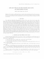
IDEAL STEP-UP (BOOST) CONVERTER
The basic step-up (boost) converter circuit is shown in Figure 3.14. During the
switch on-time, the current builds up in the inductor. When the switch is opened, the
energy stored in the inductor is transferred to the load through the diode.
The actual waveforms associated with the boost converter are shown in Figure 3.15.
When the switch is on, the voltage V
IN
appears across the inductor, and the
inductor current increases at a rate equal to V
IN
/L. When the switch is opened, a
voltage equal to V
OUT
– V
IN
appears across the inductor, current is supplied to the
load, and the current decays at a rate equal to (V
OUT
– V
IN
)/L. The inductor
current waveform is shown in Figure 3.15B.
SWITCHING REGULATORS
3.16
BASIC STEP-UP (BOOST) CONVERTER
LOAD
+
ERROR AMPLIFIER
AND SWITCH
CONTROL CIRCUIT
L
C
SENSE
SW
SW ON
SW OFF
t
on
t
off
f
t
on
t
off
==
++
1
D
Figure 3.14
BASIC STEP-UP (BOOST) CONVERTER WAVEFORMS
(SLOPES)
0
i
D
= i
OUT
i
IN
= i
L
+
LOAD
SW
L
C
v
D
i
IN
= i
L
i
D
= i
OUT
I
IN
I
OUT
V
IN
V
OUT
i
SW
V
OUT
I
IN
I
OUT
I
IN
I
IN
i
SW
v
SW
0
0
0
t
on
t
off
t
on
Lower Case = Instantaneous Value
Upper Case = Average Value
V
IN
V
OUT
L
−−V
IN
L
D
A
B
C
D
Figure 3.15
SWITCHING REGULATORS
3.17
Note that in the boost converter, the input current is continuous, while the output
current (Figure 3.15D) is pulsating. This implies that filtering the output of a boost
converter is more difficult than that of a buck converter. (Refer back to the previous
discussion of buck converters). Also note that the input current is the sum of the
switch and diode current.
If a steady-state condition exists (see Figure 3.16), the basic relationship between
the input and output voltage may be derived by inspecting the inductor current
waveform and writing:
V
IN
L
t
on
V
OUT
V
IN
L
t
off
• =
−
• .
Solving for V
OUT
:
V
OUT
V
IN
t
on
t
off
t
off
V
IN
D
= •
+
= •
−
1
1
.
INPUT/OUTPUT RELATIONSHIP
FOR BOOST CONVERTER
n Write by Inspection from Inductor/Input Current Waveforms:
n
n Rearrange and Solve for V
OUT
:
n
V
IN
L
t
on
V
OUT
V
IN
L
t
off
•• ==
−−
••
i
L
= i
IN
I
OUT
0
V
IN
V
OUT
L
−−
V
IN
L
t
on
t
off
t
on
V
OUT
V
IN
t
on
t
off
t
off
V
IN
D
== ••
++
== ••
−−
1
1
Figure 3.16
SWITCHING REGULATORS
3.18
This discussion so far has assumed the boost converter is in the continuous-mode of
operation, defined by the fact that the inductor current never goes to zero. If,
however, the output load current is decreased, there comes a point where the
inductor current will go to zero between cycles, and the inductor current is said to be
discontinuous. It is necessary to understand this operating mode as well, since many
switchers must supply a wide dynamic range of output current, where this
phenomenon is unavoidable.
Discontinuous operation for the boost converter is similar to that of the buck
converter. Figure 3.17 shows the waveforms. Note that when the inductor current
goes to zero, ringing occurs at the switch node at a frequency f
o
given by:
f
o
L C
D
C
SW
=
+
1
2 π ( )
.
BOOST CONVERTER WAVEFORMS
DISCONTINUOUS MODE
0
i
IN
= i
L
I
IN
i
SW
0
i
D
= i
OUT
I
OUT
0
V
IN
v
SW
0
t
on
t
on
t
off
V
OUT
+
LOAD
SW
L
C
v
SW
i
IN
= i
L
i
D
= i
OUT
I
IN
I
OUT
V
IN
V
OUT
i
SW
Lower Case = Instantaneous Value
Upper Case = Average Value
D
A
B
C
D
Figure 3.17
The inductor, L, resonates with the stray switch capacitance and diode capacitance,
C
SW
+ C
D
as in the case of the buck converter. The ringing is dampened by circuit
resistances, and, if needed, a snubber.
The current at which a boost converter becomes discontinuous can be derived by
observing the inductor current (same as input current) waveform of Figure 3.18.
SWITCHING REGULATORS
3.19
BOOST CONVERTER POINT
OF DISCONTINUOUS OPERATION
DISCONTINUOUS MODE IF:
(( ))
I
OUT
V
IN
V
OUT
V
IN
V
OUT
Lf
f
t
on
t
off
<<
−−
••
==
++
2
2
2
1
,
V
IN
V
OUT
L
−−
V
IN
L
I
IN
I
PEAK
t
on
t
off
INDUCTOR CURRENT AND INPUT CURRENT
0
I
IN
I
PEAK
V
OUT
V
IN
L
t
off
<< ==
−−
••
1
2 2
Figure 3.18
The average input current at the point of discontinuous operation is
I
IN
= I
PEAK
/2.
Discontinuous operation will occur if
I
IN
< I
PEAK
/2.
However,
I
IN
I
PEAK
V
OUT
V
IN
t
off
= =
−
•
2 2L
.
Also,
V
IN
I
IN
V
OUT
I
OUT
• = •
, and therefore
(
)
I
OUT
V
IN
V
OUT
I
IN
V
IN
V
OUT
V
OUT
V
IN
L
t
off
= • = •
−
•
2
.
However,
V
OUT
V
IN
D
t
on
t
on
t
off
t
on
t
off
t
off
=
−
=
−
+
=
+1
1
1
1
.
SWITCHING REGULATORS
3.20
Solving for t
off
:
( )
t
off
V
IN
V
OUT
t
on
t
off
V
IN
f V
OUT
= + =
•
.
Substituting this value for t
off
into the previous expression for I
OUT
, the criteria for
discontinuous operation of a boost converter is established:
I
OUT
V
IN
V
OUT
V
IN
V
OUT
Lf
<
−
•
2
2
2
( )
. (Criteria for discontinuous operation -
boost converter).
The basic buck and boost converter circuits can work equally well for negative
inputs and outputs as shown in Figure 3.19. Note that the only difference is that the
polarities of the input voltage and the diode have been reversed. In practice,
however, not many IC buck and boost regulators or controllers will work with
negative inputs. In some cases, external circuitry can be added in order to handle
negative inputs and outputs. Rarely are regulators or controllers designed
specifically for negative inputs or outputs. In any case, data sheets for the specific
ICs will indicate the degree of flexibility allowed.
NEGATIVE IN, NEGATIVE OUT
BUCK AND BOOST CONVERTERS
+
LOAD
SW
L
C
V
IN
V
OUT
D
+
LOAD
SW
L
C
V
IN
V
OUT
D
BUCK BOOST
+ +
Figure 3.19
SWITCHING REGULATORS
3.21
BUCK-BOOST TOPOLOGIES
The simple buck converter can only produce an output voltage which is less than the
input voltage, while the simple boost converter can only produce an output voltage
greater than the input voltage. There are many applications where more flexibility
is required. This is especially true in battery powered applications, where the fully
charged battery voltage starts out greater than the desired output (the converter
must operate in the buck mode), but as the battery discharges, its voltage becomes
less than the desired output (the converter must then operate in the boost mode).
A buck-boost converter is capable of producing an output voltage which is either
greater than or less than the absolute value of the input voltage. A simple buck-
boost converter topology is shown in Figure 3.20. The input voltage is positive, and
the output voltage is negative. When the switch is on, the inductor current builds
up. When the switch is opened, the inductor supplies current to the load through the
diode. Obviously, this circuit can be modified for a negative input and a positive
output by reversing the polarity of the diode.
BUCK-BOOST CONVERTER #1,
+V
IN
, -V
OUT
The Absolute Value of the Output Can Be Less Than
Or Greater Than the Absolute Value of the Input
LOAD
+
L
C
SW
D
V
IN
V
OUT
(NEGATIVE)
+
Figure 3.20
SWITCHING REGULATORS
3.22
A second buck-boost converter topology is shown in Figure 3.21. This circuit allows
both the input and output voltage to be positive. When the switches are closed, the
inductor current builds up. When the switches open, the inductor current is supplied
to the load through the current path provided by D1 and D2. A fundamental
disadvantage to this circuit is that it requires two switches and two diodes. As in the
previous circuits, the polarities of the diodes may be reversed to handle negative
input and output voltages.
BUCK-BOOST CONVERTER #2
+V
IN
, +V
OUT
V
OUT
(POSITIVE)
LOAD
+
L
C
SW1
D1
V
IN
SW2
D2
The Absolute Value of the Output Can Be Less Than
Or Greater Than the Absolute Value of the Input
+
Figure 3.21
Another way to accomplish the buck-boost function is to cascade two switching
regulators; a boost regulator followed by a buck regulator as shown in Figure 3.22.
The example shows some practical voltages in a battery-operated system. The input
from the four AA cells can range from 6V (charged) to about 3.5V (discharged). The
intermediate voltage output of the boost converter is 8V, which is always greater
than the input voltage. The buck regulator generates the desired 5V from the 8V
intermediate voltage. The total efficiency of the combination is the product of the
individual efficiencies of each regulator, and can be greater than 85% with careful
design.
An alternate topology is use a buck regulator followed by a boost regulator. This
approach, however, has the disadvantage of pulsating currents on both the input
and output and a higher current at the intermediate voltage output.
SWITCHING REGULATORS
3.23
CASCADED BUCK-BOOST REGULATORS
(EXAMPLE VOLTAGES)
V
IN
,
4 AA CELLS
3.5 - 6V
INTERMEDIATE
VOLTAGE
V
OUT
5V
8V
BOOST
REGULATOR
BUCK
REGULATOR
+
Figure 3.22
OTHER NON-ISOLATED SWITCHER TOPOLOGIES
The coupled-inductor single-ended primary inductance converter (SEPIC) topology is
shown in Figure 3.23. This converter uses a transformer with the addition of
capacitor C
C
which couples additional energy to the load. If the turns ratio (N = the
ratio of the number of primary turns to the number of secondary turns) of the
transformer in the SEPIC converter is 1:1, the capacitor serves only to recover the
energy in the leakage inductance (i.e., that energy which is not perfectly coupled
between the windings) and delivering it to the load. In that case, the relationship
between input and output voltage is given by
V
OUT
V
IN
D
D
= •
−1
.
For non-unity turns ratios the input/output relationship is highly nonlinear due to
transfer of energy occurring via both the coupling between the windings and the
capacitor C
C
. For that reason, it is not analyzed here.
SWITCHING REGULATORS
3.24
SINGLE-ENDED PRIMARY INDUCTANCE CONVERTER
(SEPIC)
LOAD
+
V
IN
V
OUT
C
C
C
N:1
Figure 3.23
This converter topology often makes an excellent choice in non-isolated battery-
powered systems for providing both the ability to step up or down the voltage, and,
unlike the boost converter, the ability to have zero voltage at the output when
desired.
The Zeta and Cük converters, not shown, are two examples of non-isolated
converters which require capacitors to deliver energy from input to output, i.e.,
rather than just to store energy or deliver only recovered leakage energy, as the
SEPIC can be configured via a 1:1 turns ratio. Because capacitors capable of
delivering energy efficiently in such converters tend to be bulky and expensive, these
converters are not frequently used.
ISOLATED SWITCHING REGULATOR TOPOLOGIES
The switching regulators discussed so far have direct galvanic connections between
the input and output. Transformers can be used to supply galvanic isolation as well
as allowing the buck-boost function to be easily performed. However, adding a
transformer to the circuit creates a more complicated and expensive design as well
as increasing the physical size.
The basic flyback buck-boost converter circuit is shown in Figure 3.24. It is derived
from the buck-boost converter topology. When the switch is on, the current builds up
in the primary of the transformer. When the switch is opened, the current reverts to
the secondary winding and flows through the diode and into the load. The
relationship between the input and output voltage is determined by the turns ratio,
N, and the duty cycle, D, per the following equation:
V
OUT
V
IN
N
D
D
= •
−1
.
SWITCHING REGULATORS
3.25
A disadvantage of the flyback converter is the high energy which must be stored in
the transformer in the form of DC current in the windings. This requires larger cores
than would be necessary with pure AC in the windings.
ISOLATED TOPOLOGY:
FLYBACK CONVERTER
LOAD
+
SW
D
CV
IN
V
OUT
(BUCK-BOOST DERIVED)
D = Duty Cycle
V
OUT
V
IN
N
D
D
== ••
−−1
N:1
Figure 3.24
The basic forward converter topology is shown in Figure 3.25. It is derived from the
buck converter. This topology avoids the problem of large stored energy in the
transformer core. However, the circuit is more complex and requires an additional
magnetic element (a transformer), an inductor, an additional transformer winding,
plus three diodes. When the switch is on, current builds up in the primary winding
and also in the secondary winding, where it is transferred to the load through diode
D1. When the switch is on, the current in the inductor flows out of D1 from the
transformer and is reflected back to the primary winding according to the turns
ratio. Additionally, the current due to the input voltage applied across the primary
inductance, called the magnetizing current, flows in the primary winding. When the
switch is opened, the current in the inductor continues to flow through the load via
the return path provided by diode D2. The load current is no longer reflected into
the transformer, but the magnetizing current induced in the primary still requires a
return path so that the transformer can be reset. Hence the extra reset winding and
diode are needed.
The relationship between the input and output voltage is given by:
V
OUT
V
IN
N
D= • .