đồ dàn trải ti vi màu trung quốc 4511n
Bạn đang xem bản rút gọn của tài liệu. Xem và tải ngay bản đầy đủ của tài liệu tại đây (455.15 KB, 5 trang )
MM54HC4511/MM74HC4511
BCD-to-7 Segment Latch/Decoder/Driver
General Description Features
January 1988
This high speed latch/decoder/driver utilizes advanced sili-
con-gate CMOS technology. It has the high noise immunity
and low power consumption of standard CMOS integrated
circuits, as well as the ability to drive 10 LS-TTL loads. The
circuit provides the functions of a 4-bit storage latch, an
8421 BCD-to-seven segment decoder, and an output drive
capability. Lamp test (LT), blanking (Bl), and latch enable
(LE) inputs are used to test the display, to turn-off or pulse
modulate the brightness of the display, and to store a BCD
code, respectively. It can be used with seven-segment light
emitting diodes (LED), incandescent, fluorescent, gas dis-
charge, or liquid crystal readouts either directly or indirectly.
Applications include instrument (e.g., counter, DVM, etc.)
display driver, computer/calculator display driver, cockpit
display driver, and various clock, watch, and timer uses.
The 54HC/74HC logic family is speed, function, and pinout
compatible with the standard 54LS/74LS logic family. All
inputs are protected from damage due to static discharge by
internal diode clamps to VCC and ground.
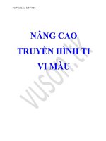
Connection Diagram
Dual-In-Line Package
TL/F/5373 – 1
Order Number MM54HC4511 or MM74HC4511
Y Latch storage of input data
Y Blanking input
Y Lamp test input
Y Low power consumption characteristics of CMOS
devices
Y Wide operating voltage range: 2 to 6 volts
Y Low input current: 1 mA maximum
Y Low quiescent current: 80 mA maximum over full tem-
perature range (74 Series)
Truth Table
INPUTS OUTPUTS
LE BI LT D C B A a b c d e f g DISPLAY
x x L x x x x H H H H H H H 8
x L H x x x x L L L L L L L
L H H L L L L H H H H H H L 0
L H H L L L H L H H L L L L 1
L H H L L H L H H L H H L H 2
L H H L L H H H H H H L L H 3
L H H L H L L L H H L L H H 4
L H H L H L H H L H H L H H 5
L H H L H H L L L H H H H H 6
L H H L H H H H H H L L L L 7
L H H H L L L H H H H H H H 8
L H H H L L H H H H L L H H 9
L H H H L H L L L L L L L L
L H H H L H H L L L L L L L
L H H H H L L L L L L L L L
L H H H H L H L L L L L L L
L H H H H H L L L L L L L L
L H H H H H H L L L L L L L
H H H x x x x
x
e
Don’t care
* *
C1995 National Semiconductor Corporation TL/F/5373
*
e
Depends upon the BCD code applied during the 0 to 1 transition of LE.
RRD-B30M105/Printed in U. S. A.
M
M
5
4
H
C
4
5
1
1
/
M
M
7
4
H
C
4
5
1
1
B
C
D
-
t
o
-
7
S
e
g
m
e
n
t
L
a
t
c
h
/
D
e
c
o
d
e
r
/
D
r
i
v
e
r
Absolute Maximum Ratings (Notes 1 and 2)
If Military/Aerospace specified devices are required,
Operating Conditions
Min Max Units
please contact the National Semiconductor Sales
Office/Distributors for availability and specifications.
Supply Voltage (VCC) b0.5 to
a
7.0V
DC Input Voltage (VIN) b1.5 to VCC
a
1.5V
Supply Voltage (VCC)
DC Input or Output Voltage
(VIN, VOUT)
Operating Temp. Range (TA)
2
0
6
V
CC
V
V
DC Output Voltage (V
OUT
) b0.5 to V
CC
a0.5V
Clamp Diode Current (IIK, IOK) g20 mA
DC Output Current, per pin (IOUT) g25 mA
DC V
CC
or GND Current, per pin (I
CC
) g50 mA
Storage Temperature Range (TSTG)
b
65§C to
a
150§C
Power Dissipation (PD)
(Note 3) 600 mW
S.O. Package only 500 mW
Lead Temp. (TL) (Soldering 10 seconds) 260§C
DC Electrical Characteristics (Note 4)
MM74HC
MM54HC
Input Rise or Fall Times
(t
r
, t
f
) V
CC
e2.0V
V
CC
e4.5V
VCC
e
6.0V
74HC
TA
e
25§C
b40
a
85
b55
a
125
1000
500
400
54HC
§C
§C
ns
ns
ns
Symbol Parameter Conditions VCC
Typ
T
A
e b40 to 85§C T
A
e b55 to 125§C Units
Guaranteed Limits
VIH
VIL
VOH
Minimum High Level
Input Voltage
Maximum Low Level
Input Voltage**
Minimum High Level VIN
e
VIH or VIL
2.0V
4.5V
6.0V
2.0V
4.5V
6.0V
1.5
3.15
4.2
0.5
1.35
1.8
1.5
3.15
4.2
0.5
1.35
1.8
1.5
3.15
4.2
0.5
1.35
1.8
V
V
V
V
V
V
Output Voltage
lIOUTl
s
20 mA
VIN
e
VIH or VIL
2.0V 2.0 1.9
4.5V 4.5 4.4
6.0V 6.0 5.9
1.9
4.4
5.9
1.9
4.4
5.9
V
V
V
V
OL
lIOUTl
s
6.0 mA 4.5V 4.2 3.98
lIOUTl
s
7.8 mA 6.0V 5.7 5.48
Maximum Low Level V
IN
eV
IH
or V
IL
3.84
5.34
3.7
5.2
V
V
Output Voltage
lIOUTl
s
20 mA
V
IN
eV
IH
or V
IL
2.0V 0 0.1
4.5V 0 0.1
6.0V 0 0.1
0.1
0.1
0.1
0.1
0.1
0.1
V
V
V
I
IN
Maximum Input
Current
lIOUTl
s
4.0 mA 4.5V 0.2 0.26
lIOUTl
s
5.2 mA 6.0V 0.2 0.26
V
IN
eV
CC
or GND 6.0V g0.1
0.33
0.33
g1.0
0.4
0.4
g1.0
V
V
mA
ICC Maximum Quiescent VIN
e
VCC or GND 6.0V
Supply Current IOUT
e
0 mA
8.0 80 160 mA
Note 1: Absolute Maximum Ratings are those values beyond which damage to the device may occur.
Note 2: Unless otherwise specified all voltages are referenced to ground.
Note 3: Power Dissipation temperature derating Ð plastic ‘‘N’’ package:
b
12 mW/§C from 65§C to 85§C; ceramic ‘‘J’’ package:
b
12 mW/§C from 100§C to 125§C.
Note 4: For a power supply of 5V
g
10% the worst case output voltages (V
OH
, and V
OL
) occur for HC at 4.5V. Thus the 4.5V values should be used when
designing with this supply. Worst case V
IH
and V
IL
occur at V
CC
e5.5V and 4.5V respectively. (The V
IH
value at 5.5V is 3.85V.) The worst case leakage current (I
IN
,
I
CC
, and I
OZ
) occur for CMOS at the higher voltage and so the 6.0V values should be used.
**VIL limits are currently tested at 20% of VCC. The above VIL specification (30% of VCC) will be implemented no later than Q1, CY’89.
2
AC Electrical Characteristics V
CC
e5V, T
A
e25§C, C
L
e15 pF, t
r
et
f
e6 ns
Guaranteed
Symbol Parameter Conditions Typ
Limit
Units
t
PHL
, t
PLH
Maximum Propagation
Delay from Inputs A thru D to any Output
tPHL, tPLH Maximum Propagation
Delay from BI to any Output
tPHL, tPLH Maximum Propagation
Delay from LT to any Output
60
60
60
120
120
120
ns
ns
ns
tS
tH
t
W
Minimum Setup Time
Inputs A thru D to LE
Minimum Hold Time
Inputs A thru D to LE
Minimum Pulse Width
for LE
10
b3
20
0
16
ns
ns
ns
AC Electrical Characteristics CL
e
50 pF, tr
e
tf
e
6 ns (unless otherwise specified)
74HC
TA
e
25§C
54HC
Symbol Parameter Conditions VCC
Typ
TA
e b
40 to 85§C TA
e b
55 to 125§C Units
Guaranteed Limits
tPHL, tPLH Maximum Propagation LE
e
0V
2.0V 300 600 756 894 ns
Delay from Inputs
LT
e
VCC 4.5V 60 120
151 179 ns
A thru D to any Output BI
e
VCC 6.0V 51 102
t
PHL
, t
PLH
Maximum Propagation LT
e
V
CC
2.0V 300 600
129
756
152
894
ns
ns
Delay from BI to
any Output
t
PHL
, t
PLH
Maximum Propagation BI
e
0V
Delay from LT to
any Output
4.5V 60 120
6.0V 51 102
2.0V 300 600
4.5V 60 120
6.0V 51 102
151
129
756
151
129
179
152
894
179
152
ns
ns
ns
ns
ns
tS
tH
tW
t
r
, t
f
C
PD
CIN
Minimum Setup Time
Inputs A thru D to LE
Minimum Hold Time
Inputs A thru D to LE
Minimum Pulse Width
for LE
Maximum Input Rise and
Fall Time
Power Dissipation
Capacitance (Note 5)
Maximum Input
Capacitance
2.0V
4.5V
6.0V
2.0V
4.5V
6.0V
2.0V
4.5V
6.0V
2.0V
4.5V
6.0V
100
20
17
0
0
0
80
16
14
1000
500
400
5 10
126
25
21
0
0
0
100
20
17
1000
500
400
10
149
30
25
0
0
0
120
24
20
1000
500
400
10
ns
ns
ns
ns
ns
ns
ns
ns
ns
ns
ns
ns
pF
pF
Note 5: C
PD
determines the no load dynamic power consumption, P
D
eC
PD
V
CC
2 f
a
I
CC
V
CC
, and the no load dynamic current consumption, I
S
eC
PD
V
CC
f
a
I
CC
.
3
INPUTS
A, B, C, D (Pins 7, 1, 2, 6)ÐBCD data inputs. A (pin 7) is the
least-significant data bit and D (pin 6) is the most significant
bit. Hexadecimal data A – F at these inputs will cause the
outputs to assume a logic low, offering an alternate method
of blanking the display.
OUTPUTS
a – gÐDecoded, buffered outputs. These outputs, unlike the
4511, have CMOS drivers, which will produce typical CMOS
output voltage levels.
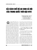
Output Characteristics (VCC
e
5V)
TL/F/5373 – 2
*The expected minimum curves are not guarantees, but are design aids.
Typical Applications
TL/F/5373 – 4
Typical Common Cathode LED Connection
4
CONTROLS
BI (Pin 4)ÐActive-low display blanking input. A logic low on
this input will cause all outputs to be held at a logic low,
thereby blanking the display. LT is the only input that will
override the Bl input.
LT (Pin 3)ÐActive-low lamp test. A low logic level on this
input causes all outputs to assume a logic high. This input
allows the user to test all segments of a display, with a
single control input. This input is independent of all other
inputs.
LE (Pin 5)ÐLatch enable input. This input controls the 4-bit
transparent latch. A logic high on this input latches the data
present at the A, B, C and D inputs; a logic low allows the
data to be transmitted through the latch to the decoder.
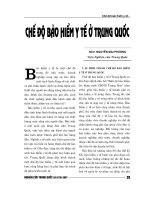
TL/F/5373 – 3
TL/F/5373 – 5
Incandescent Bulb Driving Circuit
Logic Diagram
Display
Segment Identification
TL/F/5373 – 8
5
TL/F/5373 – 6
TL/F/5373 – 7