MANAGING POWER ELECTRONICS VLSl and DSP-Driven Computer Systems phần 3 docx
Bạn đang xem bản rút gọn của tài liệu. Xem và tải ngay bản đầy đủ của tài liệu tại đây (1.97 MB, 41 trang )
Buck
Converters
61
A,
=
6.28
x
30 kHz
x
3.6 pH13 mQ
=
226
Eq.
3-80
We know the
ESR
zero to be at
1
kHz
fZESR
=
kHz
Eq.
3-81
and
fpLc=
1/27~(LC)”*
=
116.28
x
4.3
x
lo4
=
10000127
=
370 Hz
Eq.
3-82
and given
VIN=
12
V,
VCT=
1
V,
a=
1,
andGM= 26pN26 mV
=
111 kQ
we have
Rc= 226
x
1
kQ112
=
19 kR
Eq.
3-84
Now from
fzc
=
1
127~RCCc
Eq.
3-85
settingfic at 37 Hz
(
1
Ox
below the
LC
double pole) we have
C,
=
116.28
x
19 kR
x
37
=
0.22
pF
=
220 nF
Eq.
3-86
And
so
all the main parameters of the control loop are set.
Input
Filter
The input current is chopped
as
indicated in Figure 3-29
so
it will need
some input filtering.
Input
Inductor
LIN
Assuming that at the input we need a current smoothed down to
0.1
Alps
with an input voltage ripple of
0.5
V, we have
dV
=
0.5
V
Eq.
3-87
dlldt
=
0.1
Alps
Eq.
3-88
62
Chapter
3
Circuits
Figure
3-29
Input filter.
and from
LIN
x
dlldt
=
dV
'OUT
Eq.
3-89
LIN
=
0.5
Vl(0.1
Alps)
=
5
pH
Eq.
3-90
Input Capacitor
1=20A
Eq.
3-91
Eq.
3-92
dlldt
=
0.1
Alps
hence the time to build
up
20 A
in
the inductor is, from
Eq.
3-89
dT
=
20 Al(0.
1
Alp)
=
200
ps
Eq.
3-93
From the formula
CIN
x
dVldt
=
I
Eq.
3-94
Knowing that
dVldt
=
0.5
Vl200
ps
=
2.5
Vlms
C
=
20 Al(2.5
Vlms)
=
8
mF
Eq.
3-95
Eq.
3-96
This capacitor has to sustain an
RMS
current defined as a function of
the
DC
and peak current as follows:
IRMs
=
I(DC
-
DC2)'12
Eq.
3-97
from which
IRMs
=
20(0.1
-
0.01)1/2
=
20
x
0.091/2
=
20
x
0.3
=
6
A
Eq.
3-98
It is important to select the input capacitor capable of carrying the cal-
culated
RMS
current.
Buck Converters
63
Current Mode
So
far we have analyzed control schemes based on a single control loop, the
voltage control loop setting the output voltage. In any regulator when the
output is low-say at start-up-the pass transistor will keep charging the
output capacitor via the inductor until the output reaches final value. Dur-
ing this phase the voltage across the inductor is
VIN
-
VoUr
and the current
is building in the inductor at a rate
[(VIN
-
VoUT)/L]
x
t.
If
this phase lasts
too long, the current build up inside the inductor can be excessive. One way
to control such build up is cycle-by-cycle current control using a secondary
current control loop nested inside the primary voltage control loop. In the
current control loop illustration in Figure
3-30
the current in the inductor is
limited to
VIRDsop
Peak Current Control
Figure
3-30
Current mode illustration.
Another interesting outcome is that now the entire block from the
V
voltage node to the
I,
current node (inductor current) becomes a simple
trans-conductance block with a transfer function that is simply
~/RD,,N
It follows that from a small signal analysis stand point, the inductor
effect in the loop is effectively bypassed; the open loop gain loses the LC
double pole and is left with only the
COuT
single pole. In this case the
expression of the open loop gain becomes
AOL
=
A"/@C
X
RDSoN)
Eq.
3-100
This is a very simple expression compared to
Eq.
3-77.
A
more com-
plicated circuit yields a simpler transfer function! It follows that in princi-
ple a current mode regulator should be easier to compensate compared
to
a
plain voltage mode control loop.
64
Chapter
3
Circuits
In this section we have covered some fundamental aspects
of
switching
regulators and some general techniques for their analysis. With the tools
provided we should be able to pick
a
PWM controller and match
it
to
the
power train and compensation elements. With this foundation the reader
can venture into more complex aspects of circuital architecture including
leading and trailing edge modulation
valley and peak current control
PWM versus PFM versus hysteretic control
Some of these aspects are discussed in the following chapters. For
other aspects not covered here the reader should refer to the references
in
the further reading section at the end of this book.
3.9
Flyback
Converters
Figure 3-3
1
shows
a
simplified block diagram of
a
flyback converter
power train. In this voltage mode flyback architecture the energy is stored
in the transformer when the switch SW is on and transferred to the load
when the switch is off.
The use
of
a
transformer with
a
turns ration of n:
1
allows
a
lot of free-
dom
as
far
as
input versus output value setting. In
a
flyback converter the
transformer stores energy during the
on
time of the SW
1
transistor. The
inductor windings are coupled
in
such
a
way (opposite windings as indi-
cated by the dots on each transformer winding) that voltage on the two
windings are of the opposite sign. This arrangement, coupled with the
placement of diode
D
(we will approximate the forward drop
of
the diode
to zero), is such that when current flows
in
the primary winding,
it
cannot
flow in the secondary. Accordingly the energy associated with the primary
current cannot be transferred to the secondary and
it
is stored
in
the trans-
former air gap. When the switch is open, the current ceases to circulate
in
the primary and the energy stored in the transformer gap releases via
a
cur-
rent in the secondary. If the voltage on the secondary is
VouT
(assured by
the control loop not shown here) then this voltage will reflect back on the
primary via the turns ration, hence the voltage across the transformer pri-
mary will be
-nVo.
This voltage subtracts to
VfN
so
that the final voltage
across the open switch SW during the
off
phase is
Vsw
=
VfN
-
(-nVo)
=
VIN
+
nVo
Eq. 3-101
This observation is important because the switch SW is most likely
going to be
a
DMOS
transistor and its voltage rating will have to be
Flyback
Converters
65
‘sw
‘R
drk
VS
“IN,,
Figure
3-31
Flyback converter simplified block diagram and waveforms.
selected to be safely above
VIN
+
nVo. On the secondary side, the average
of the secondary current waveform
I,
is the load current. The picture
shows the case of light load, with secondary current reaching zero when
the primary switch
SW
is still off. In the absence of current on the second-
ary there is no voltage on the secondary and no reflected voltage
on
the
primary side, hence during this time interval the voltage across the pri-
mary winding is zero and the voltage across the switch
SW
is simply
VIM
The control loop and its analysis techniques are similar to the one dis-
cussed for the buck converter and will not be repeated here.
The other advantage of the transformer, besides input-to-output volt-
age ratioing, is isolation. In high voltage applications isolation is
mandatory not only in the forward path, but also in the feedback path. For
this reason transformers
in
the forward path are a must in offline applica-
tions, while
in
the feedback path often opto-couplers (Figure
3-32)
are uti-
lized for signal isolation. In an opto-coupler the photo-diode emits light
proportionally to its bias current.
A
portion of this light hits the corre-
sponding phototransistor which in turn produces a current variation pro-
portional to the incoming light. Since the coupling mechanism is based on
light, the opto-coupler works with
AC
as well as
DC
feedback signals. In
the following chapters we will encounter a few examples of such isolated
architectures.
A
conventional transformer is called to transfer energy, not store it,
so
it
does not normally have an
air
gap,
which is the place where energy is stored.
In
the flyback configuration, the transformer is hybridized to have an air gap
and store energy as discussed earlier. For this reason this “transformer” is also
referred
to
as a “coupled inductor” since the two windings, due to the energy
storage twist, act essentially like inductors. Figure
3-33
is a nice illustration
of
the transformer femte core and its energy storage air gap.
66
Chapter
3
Circuits
Figure
3-32
Symbol of opto-coupler.
Figure
3-33
Gapped transformer illustration.
As
with non-isolated converters, there is a long list
of
isolated con-
verter architectures as well. We will encounter some of these architectures
in the next chapters. For a more systematic treatment of these architectures
the reader can refer to the provided references.
Part
II
Digital Circuits
In this section we will discuss some fundamental digital building blocks
for power management. We will quickly review the main properties of the
elementary components, the logic gates,
so
that we can use them to build
higher level functions like flip-flops, shift registers, and communications
input and output functions. There are many good reasons to mix analog
and digital circuits. Soon we will see an example where adding
a
flip-flop
to an analog regulation loop improves the noise insensitivity of the circuit.
Logic Functions
67
Today's power management devices are often externally driven by a
central processing unit. In order to interface with such
CPUs,
power man-
agement chips may include
on
board some or all of the logic elements
mentioned above
in
the form
of
input-output communications cells.
Finally digitalization
of
power, as will be discussed
in
detail later, is
another reason for
a
mixed analog and digital approach to power
management.
3.1
0
Logic Functions
NAND
Gate
In Figure
3-34
we have a fundamental logic block, the
NAND
gate
with its
symbol,
CMOS
implementation, and truth table, the equivalent
of
the
input to output transfer function we have for an analog block. The truth
table can be easily proven by exercising it
on
the
CMOS
implementation
schematic.
"cc
TI
?
T2
-
C=A’B
I
0-
*
T3
__c_(
T4
Figure
3-34
Logic
NAND
gate (a) symbol, (b)
CMOS
implementation,
and (c) truth table.
68
Chapter
3
Circuits
Set-Reset
R
Flip-Flop
In Figure
3-35
we have put
to
use the NAND gates to build
a
Set-Reset
Flip-Flop,
or to be more precise,
a
Set#-Reset# one
(#
stands for the nega-
tion bar), the most elementary memory cell. In the truth table
M
stands for
the memory state; when Set#
=
Reset#
=
1
the output stays in the previous
state. Naturally one inverter in front of each input will produce a Set-Reset
Flip-Flop with the table shown in Figure
3-36.
(a)
(b)
Figure
3-35
Set#-Reset# Flip-Flop (a) logic schematic and (b) truth table.
(a)
(b)
Figure
3-36
Set-Reset Flip-Flop
(a)
symbol and (b) truth table.
Current Mode with Anti-Bouncing
Flip-Flop
In Figure
3-37
we have put to use the Set-Reset Flip-Flop by inserting it
into the current mode voltage control loop from Figure
3-30.
The circuit
in
Figure
3-30
is subject to noise as the comparator can be triggered by
any noise spike at any time. By inserting the flip-flop in the loop we create
Logic Functions
69
a synchronous system that is insensitive to noise. In fact, from Figure
3-37
and the table in Figure 3-36(b) we see that once reset is triggered (a spike
to one and back to zero) the flip-flop is in a memory state until the next set
spike. Hence a new charging cycle cannot be initiated by false triggering
of
the comparator.
Peak
Current
Control
LRIPPLE
V,
IL.RDSON
CLOCK
=
SET
COMPO
=
RESET
PWM
Figure
3-37
Current control with anti-bounce Set-Reset Flip-Flop.
This Page Intentionally Left Blank
In
the first two sections of this chapter, we will discuss
in
detail two
buck converter cases. The first case is
a
high current buck converter for
desktop, handling high current and thus requiring external power
MOS-
FET transistors. The emphasis here will be on the advantages of
a
spe-
cific architecture for this application, called
vulley
control.
The second
case is
a
low current buck converter for ultraportable applications. For
such low power applications, the power transistors are integrated on
board.
In
this case, the emphasis is on the design methodology and fast
time to market.
In
the third section we will discuss the active clamp,
a
method to deliver instantaneous power to the load bypassing the output
filter. This method is advantageous because the filter slows down the
response of
a
regular buck converter regardless of the speed of the front
end silicon. In the fourth section we will discuss battery charger system
architecture for notebooks. Finally
in
the fifth section we will cover the
subject of digital power, a new trend of implementing power with digital
techniques
in
place of traditional analog ones.
4.1
Valley Control Architecture
Modern CPUs require very low voltage
of
operation
(1.5
V
and below)
and very high currents (up to
100
A).
Such power comes more and more
frequently from the
silver
box,
a power supply device typically used
inside a desktop PC box that provides all the necessary offline power to
the PC electronics. With a buck converter, this application results
in
very
low duty cycle,
on
the order of
0.1
V/V,
which stretches the limit of
71
72
Chaoter
4
DC-DC Conversion Architectures
performance of the conventional
peak current-mode control
architec-
ture. The proposed valley control technique brings new life to the buck
converter application, allowing
it
to meet present day specifications more
easily as well as remain a viable solution
in
the future.
Peak and Valley Control Architectures
This section describes the two different architectures illustrated
in
Figure
4-
1.
Peak Current-Mode Control Based on Trailing Edge Modulation
In normal closed-loop operation, the error amplifier forces
VouT
to equal
VREF
at its input, while at its output the voltage
V,
is compared to the
high side MOSFET current
(IL)
multiplied by
RDsoN
(on resistance of the
DMOS). When
I,
x
RDsoN
exceeds the error voltage, the PWM compara-
tor flips high, resetting the flip-flop and consequently terminating the
charge phase by turning
off
the high side driver and initiating the dis-
charge phase by turning on the low side driver. The discharge phase con-
tinues
until
the next clock pulse sets the flip-flop, initiating a new
charging phase.
Valley Current-Mode Control Based on Leading Edge
Modulation
Vulley current-rnode control
operation mirrors that of peak current-mode
control, but
it
has significant advantages. In normal closed-loop operation,
the error amplifier forces
VouT
to
equal
VREF
at its input, while at its out-
put its voltage
V,
is compared
to
the low side MOSFET current
(IL)
times
RDsoN
(notice that
in
the previous case
V,
is compared
to
the high side
MOSFET current). When
I,
x
RDsoN
falls below the error voltage, the
PWM comparator flips high, setting the flip-flop and consequently initiat-
ing the charge phase by turning on the high side driver and terminating the
discharge phase by turning off the low side driver. The charge phase con-
tinues
until
the next clock pulse resets the flip-flop, initiating a new dis-
charging phase.
Current Sensing
The fact that valley current-mode control relies on sensing of the decay-
ing current (the current
in
the low side MOSFET) has one useful implica-
tion for current sensing.
If
lossless current is implemented, the sensing is
done across the low side MOSFET, which is normally
on
for
90
percent
of
the time in this type of application. Since the on-time of the low side
Valley
Control
Architecture
73
CK
-
f
I
Peak
Control
v,
CK
-
-+
+
RUSONI’L
A,=
1
Valley
Control
IRlPPLE
VF
‘,^RUSON
CLOCK
=
SET
COMPO
=
RESET
PWM
COMPO
=
RESET
PWM
Figure
4-1
Peak and valley control.
MOSFET
is almost ten times wider than that of the high side MOSFET,
sampling and processing of the low side device current are much easier to
accomplish
in
comparison to high side sensing. Sensing
of
the high side
current at low duty cycles is
so
undesirable that some solutions
in
the mar-
ket have been based on sensing low side current
and
a
trailing edge current
control strategy. However, the current information comes after the fact-
namely after the current has peaked, has started the decaying phase, and
can be utilized for cycle-by-cycle peak current control only at the next
cycle.
In
addition
to
sampling the current, a mechanism must be provided
to hold the sampled information until the next cycle. The sample-and-hold
mechanism adds complexity
to
the circuitry. and more importantly adds
a
delay
or
phase shift, which tends
to
compromise the frequency stability
of
the control loop.
Maximum Frequency
of
Operation
In
the case of very low duty cycle operation with either valley
or
peak cur-
rent-mode control, the maximum frequency of operation is limited by the
minimum possible on-time
of
the high side driver. While
in
both cases the
74
Chapter
4
DC-DC
Conversion Architectures
same set
of
initial physical limitations determines the high side driver min-
imum pulse width, the peak current-mode control has in addition
a
limit-
ing settling time requirement, namely the pulse must be wide enough to
allow the current to be measured. This additional limitation applies to the
cases of lossless high side sensing and to sensing with a discrete high side
sense resistor.
Frequency of Operation for Peak Current-Mode Control
Assuming that the settling time for sensing the high side current is
ToNp-
MIN
=
100
ns, then with DC
=
0.1
VN,
we have
a
minimum period of oper-
ation
TMiNp
TMINp
=
ToNp-MINIDC
=
100
nsl0.l
=
1
ps
which corresponds to
a
maximum frequency of operation
Frequency of Operation for Valley Current-Mode Control
In
valley current-mode control where we sample the low side current, the
limitation discussed above is
far
less strict. Assuming an analogous mini-
mum pulse width for the low side device,
TMINV
=
T~NV
MINI(
1
-
DC)
=
100
ns10.9
=
1
10
ns
which corresponds to
a
maximum frequency of operation
fMAxv=
111
10
ns
=
9
MHz
The converter still has
to
meet the constraint of minimum on-time
of
the
high side driver. Transition times of
10
ns and below are obtainable
today. Assuming a minimum on-time of the high side device of two transi-
tion times. we have
TMlNHV
=
ToNHv-
MINIDC
=
20
ns1O.
1
=
200
ns
This yields
a
maximum frequency
of
operation,
fMAXHV
=
llTMINHV
=
MHz
Valley Control Architecture
75
'c,
Tdelay
While today's conventional monolithic and discrete technologies do
not permit practical operation at such a high clock rate, it appears that
as
these technologies improve, only valley current mode control will be able
to
easily track the speed curve and operate at such high frequencies.
Transient Response
of
Each System
In
this section we discuss the transient response
of
the two systems. The
advantages of valley control are obvious from Figure
4-2.
This system is
inherently fast and able to turn
on
immediately
in
response to
a
step cur-
rent, as opposed to peak control, where a delay
(TDELAy)
as high
as
a full
clock period is to be expected. In both cases the current ramps up (builds
up linearly inside the inductor) with
a
slope that
is
determined by the
inductance and saturated voltage appearing across the inductance and lim-
ited by the maximum duty cycle
DC,,,.
Peak
Current
r
Steady State Ripple Current
t
/
/
Positive Current
I
Step
/=/
Current in Peak Control
Figure
4-2
Positive current step.
As
an
example,
if
the clock is
700
kHz per phase,
a
full period delay
corresponds to
1.5
ps.
Traditional peak current-mode control architecture will need enough
output capacity to hold up
for
one extra
1.5
ps
in comparison to valley cur-
rent-mode control. Consider for this example that an output capacitor of
l
mF will discharge an extra
100
mV with a
65
A
load in
1.5
ps.
The comparative responses to a negative load current step are illus-
trated
in
Figure
4-3.
Here again the advantage
of
valley control architec-
ture is evident. During
a
negative load current step, the valley control
scheme is able to respond with zero duty cycle.
On
the other hand, after
76
ChaDter
4
DC-DC Conversion Architectures
Steady State Ripple Current
Out
DC
=
0
HSD
DC
=
0
Inductor Current in Vallev Control
Figure
4-3
Negative current step.
each clock pulse with peak current-mode control, the controller forces a
minimum width high side on-time. This minimal on-time is determined by
the speed of the current control loop. Thus, it is seen that the valley control
scheme offers superior transient response with
a
negative load step as well.
Valley
Control
with
FAN5093
The FAN5093 is a two-phase interleaved buck controller IC that implements
the valley control architecture based on leading edge modulation. The cur-
rent normally is sensed across the low side MOSFET
RDsoN
(for lossless
current sensing); although for precision applications
a
physical sense resis-
tor can be placed in series with the source of the low side MOSFET.
Figure
4-4
shows the two PWM switching nodes of the two-phase
buck converter, with the FAN5093 clocking each phase at
a
frequency
of
700
kHz.
In
Figure 4-5 we show the response of the voltage regulator to
a
25
A
per phase positive current step.
In Figure 4-6 we show the response of the voltage regulator to a 25
A
per phase negative current step.
Figure 4-7 shows the FAN5093 application and highlights the two-
phase interleaved architecture of this buck converter. Multiphase is
discussed
in
more detail
in
Chapter 7. As evidenced in Figure 4-4,
interleaving
consists of phasing the two channels
180
degrees apart
so
the
load current is provided in
a
more time-distributed fashion, leading to
lower input and output ripple currents. In other words, if the load is too
high
to
be handled by a single phase, there are two ways to solve the prob-
lem. The more traditional way is brute force:
to
beef up the circuit by par-
alleling
as
many MOSFETs
as
necessary. The new concept introduced by
multiphase is interleaving, to take the same numbers of transistors that we
Valley
Control
Architecture
77
I
I
1
., , ,
*
i
_._ _._._
' _
, ,
I.
,.
2
Aoav
2001
12:16
19
Figure
4-4
Interleaved buck converter:
VIN
=
12
V,
VouT
=
1.5
V,
fCK
=
700
kHz per phase.
Top
waveform: switching node of
Phase
1.
Bottom waveform: switching node of Phase
2.
I
L
1
I
C1
Freq
7
14.284kHZ
LOW
resolution
2
May
2001
12:54:58
Figure
4-5
Regulator response
to
a
positive current step.
Top
waveform:
switching node
of
Phase
1.
Bottom waveform: Phase
1
current.
wanted to parallel and operate them
out
of phase. Now we have reduced
input and output ripple, and hence we can get by with smaller input and
output passives.
The
IC
whose die layout is shown in Figure
4-8
incorporates the controller
and the drivers and works
in
conjunction with an external
DMOS
transistor
78
Chapter
4
DC-DC Conversion Architectures
C1
Freq
716.476kH2
LO
w
resolution
2
May
2001
12.50.19
Figure
4-6
Regulator response to a negative current step. Top waveform:
switching node of Phase
I.
Bottom waveform: Phase
1
current.
I
FAN5093
R16
f
Monolithic Buck
Converter
79
4.2
to handle 30 A with
3.3
V.
For further details,
a
full
data sheet of the
FAN5093 is provided
in
Appendix A. The IC is built
in
a 30
V,
0.8
pm
BiCMOS mixed signal process with excellent Bipolar and CMOS
performance.
Figure
4-8
FAN5093 die picture.
Conclusion
We have shown that the valley current-mode control buck architecture
based on leading edge modulation has superior transient response charac-
teristics when compared to the traditional peak current-mode control buck
architecture based on trailing edge modulation. These transient response
characteristics translate directly
into
a
reduced number of output capacitors
and consequently lead to a more cost-effective solution
in
a smaller board
space. This advantage, while already measurable today, will become more
marked
in
the future when progress in discrete and controller technologies
will enable multi-MHz frequencies of operation at reasonable efficiencies.
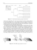
Monolithic Buck Converter
A
New Design Methodology for Faster Time
to
Market
Until recently, the prototype of a new power management subsystem
would be built
only
after its various components were physically avail-
able for prototype construction. However, a new trend is emerging, where
a
virtual prototype
is built by the subsystem manufacturer
far
ahead
of
the
80
Chapter
4
DC-DC Conversion Architectures
availability
of
physical components. From a power chip designer's perspec-
tive, the benefit is that a good behavioral model of the voltage regulator can
be utilized prior
to
the transistor-level design, reducing time-consuming
full-chip simulations to a minimum. From the system designerhstomer's
perspective, the benefit
is
that behavioral models will be available far ahead
of final silicon. Therefore, the system designer can quickly test his virtual
subsystem using behavioral simulations to provide timely feedback
to
the
chip designer before the chip is frozen
into
silicon. When the physical sub-
system prototype is finally built, testing and debugging will be much faster
and easier
to
finalize thanks
to
the previous virtual iterations.
In
the model (Figure
4-9),
the platform designer launching the system
Px at time zero will wait six months for delivery of silicon Sx+l for his
next platform Px+l. But the designer could immediately obtain behavioral
models of the silicon Sx+l from the silicon vendor, who is already twelve
months into the development cycle of that silicon.
Since Moore's law seems to hold well
no
matter what, the end result
should be an improvement
in
productivity rather than a reduction in the
development cycle. This results
in
a higher number of platform varieties
launched
in
a
unit
of time.
I
I
t
=
Delivery
of
Silicon
r
-30
-24 -18 -12
-6
0
6
12 18 24
Figure
4-9
Development cycle time model
The
Design
Cycle
This section explores the various steps of designing the controller for a
buck converter, from the construction of a simple behavioral macro model
and the subsequent transistor-level Simulation Program with Integrated
Circuit Emphasis (SPICE) simulation
to
the silicon implementation. The
time duration for each phase is also discussed. Finally, we will compare
the waveforms obtained with behavioral simulation versus
SPICE
simula-
tions and pictures taken at the oscilloscope from the physical prototype.
We will see that the three different methods produce quite similar results.
Monolithic Buck Converter
81
The
FAN5301
Figure
4-
10
shows the block diagram of the FAN530
1,
a high-efficiency
DC
to
DC
buck converter, while Figure
4-1
1
shows the application. The
architecture provides for high efficiency under light loads and at low input
voltages, as well as optimum performance at
full
load. Further detail is
provided
in
a later discussion of the behavioral block diagram.
"IN
SD
FB
REF
AGND
REFERENCE
FAN5301
Comp
Figure
4-1
0
FAN530
I
block diagram.
-
"IN,
-
sw
-
GND
out
Figure
4-1
1
FAN530
1
application.
82
ChaDter
4
DC-DC Conversion Architectures
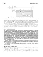
The Behavioral Model
Figure
4-12
shows the behavioral model
of
the entire power supply, com-
plete with the controller as well as the external components. The controller
is based on a minimum on-time, minimum off-time architecture.
Figure
4-12
Voltage regulator model.
Light Load Operation
The main control loop
in
light load operation is the minimum on-time sec-
tion
in Figure
4-12,
consisting
of
a
hysteretic compurutor
(Compl) that
controls a “one shot” circuit
(MIN-ON
One Shot) and driving the high
side
PMOS
switch
M
1.
The one shot circuit fires
on for
a duration
of
time
that remains steady at constant input voltage and increases as the voltage
across the pass transistor
(
VIN
-
Vour)
decreases.
During on-time, the high side driver transistor
M
1
is turned
on for
a
duration equal
to
the one shot
(MIN-ON
One Shot) on-time, and then
turned
off.
When
M
1
turns
off,
M2
is turned
on
until the inductor current
goes
to
zero, at which point both transistors are turned
off
until the output
voltage
falls
below
a
set threshold. At this point the one shot fires again,
initiating another cycle.
Monolithic
Buck
Converter
83
Full Load Operation
In
full
load, the minimum on-time block is bypassed by the hysteretic
comparator (Compl), which forces the output to swing with a ripple equal
to
the comparator hysteresis. At full load, the current in the inductor is
continuous and the operation is synchronous.
Over-Current
The minimum off-time one shot (MIN-OFF One Shot) in Figure 4-12 is
controlled with a cycle-by-cycle current limit comparator (Comp3) that
samples the current flowing through M1 via
RSENSE.
In over-current, the
high side driver is turned off for the time that is set by the MIN-OFF One
Shot. The high side driver is then turned back on.
If
the over-current per-
sists, MI is turned off again after a short time set by the Comp3 and
MIN-OFF One Shot loop delay.
Completing the circuit shown in Figure 4-12 is an under voltage lock-
out circuit (UVLO block) and a precision-trimmed band-gap reference
(VREF
block).
One
Shot
To illustrate the level of complexity of the regulator behavioral model,
Figure 4-13 dives into a representation of the MIN-ON One Shot device
shown
in
Figure 4-1 2. The one shot consists
of
a current source
IRA~P
that
charges
a
capacitor C
1,
which can be reset via the switch
S
1.
The compar-
ator “looks” at the ramp level with respect
to
the control reference voltage
CONT. The ramp time provides the duration of the output pulse.
Comparator
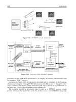
Delving further down into the nesting of the controller, Figure 4-14 shows
the block diagram of the comparator Comp
in
Figure 4-13. The PSPICE
(a popular brand and flavor
of
SPICE) behavioral model of the comparator
uses “primitive” SPICE-level blocks (like the one
in
Figure 4-15).
A
sum-
ming block follows the inverting stage into the GLIMIT
(or
gainholtage
limiter), into the inverter, and then into the output. The GLIMIT function
provides the comparator gain while the limit function allows the designer
to restrict the voltage output to a reasonable range, like
0-5
V. The resistor
provides some convergence help.
A
SPICE
deck
like the one
in
Figure 4-15 describes each primitive
functional block
in
Figure 4-14.
84
Chapter
4
DC-DC
Conversion Architectures
CLK
I
IN-
-
V
;
I
Comp
GLlMlT
-
OUT
*
Figure
4-13 Model
of
a
one shot device.
Gain
=
10000
Figure
4-14 Comparator behavioral model.
Results
The waveforms
in
Figure
4-16
show the transient response of the regula-
tor
to
a
step function
load
from
0
mA
to
100
mA
as
produced by the
behavioral simulation. Input voltage is
3.3
V
and output voltage is
1.25
V.
The graph
in
Figure
4-17
shows the same transient response from
a
transistor-level SPICE simulation (Spectre on Cadence platform). Finally,
Figure
4-1
8
illustrates the same transient from the physical prototype.
Monolithic
Buck
Converter
85
IOo.r
SLLII:
o*
2
Figure
4-15
GLIMIT SPICE deck
Although the corresponding waveforms
in
Figures 4-16,4-17, and 4-18
are not identical, they are sufficiently similar to infer consistent functional
behavior from each. Some
of
the differences can be attributed to the
unavoidable variation
on
the external components such as inductor parasit-
ics, capacitor ESR/ESL, and noise (in the case of Figure 4-18). Also com-
plicating the comparison is the fact that the laboratory equipment cannot
duplicate the instantaneous current load change the way that simulations
can. On the simulation side, differences
in
SPICE operating parameters
(Spectre versus PSPICE) and sampling can affect the output wave shapes
due to interpolation and sampling errors.
Figure
4-1
6
Transient response from behavioral model.
Top Trace:
ILoAD
0-
100
mA
Middle Trace:
VouT
Bottom Trace:
SWpin