Carbon Materials for Advanced Technologies Part 3 potx
Bạn đang xem bản rút gọn của tài liệu. Xem và tải ngay bản đầy đủ của tài liệu tại đây (632.3 KB, 35 trang )
50
of a strong electron-vibration interaction.
Optical transitions between the
HOMO and LUMO levels can thus occur through the excitation of
a
vibronic
state involving the appropriate odd-parity vibrational mode [68, 69, 70, 711.
Because of the involvement of
a
vibrational energy in the vibronic state, there
is an energy difference between the lowest energy absorption band [67] and
the lowest energy luminescence band [71].
Using these molecular states, the weak absorption observed between 490 and
640 nm for
c60
in solution (Fig. 6) [67] is assigned to transitions between the
singlet ground state
SO
and the lowest excited singlet state
SI
(associated with
the
tl,
orbital and activated by vibronic coupling).
For
C70,
molecular orbital calculations [60] reveal
a
large number
of
closely-
spaced orbitals both above and below the HOMO-LUMO gap [60]. The large
number of orbitals makes it difficult to assign particular groups of transitions
to structure observed in the solution spectra of
c70.
UV-visible solution
spectra for higher fullerenes
(C,;
n
=
76,78,82,84,90,96) have also been
reported [37, 39, 721.
Further insight into the electronic structure of fullerene molecules is pro-
vided by pulsed laser studies of
Ceo
and
(270.
Such time-resolved studies
of fullerenes in solution have been used to probe the photo-dynamics of the
optical excitation/luminescence spectra.
The importance of these dynamic
studies is to show that photo-excitation in the long-wavelength portion of the
UV-visible spectrum leads to the promotion of
C60
from the singlet
SO
ground
state
(IAg)
into a singlet
SI
excited state, which decays quickly with
a
nearly
100% efficiency [73, 741 via an inter-system
(ie,
S,
+
T,)
crossing to the
lowest excited triplet state
TI.
This rapid singlet-triplet decay (-33 ps [74]) is
fostered by the overlap
in
energy between the vibronic manifold of electronic
states associated with the lowest singlet
SI
state and the corresponding vi-
bronic manifold for the triplet
TI
state, and the very weak spin-orbit coupling
mentioned above.
For higher energy optical excitations, once
in
the
Ti
triplet excitonic manifold,
a
very rapid transition occurs to the lowest level of the
TI
triplet manifold,
about
1.55
eV above the ground state energy. The
TI
state is a metastable
state. It lies
-0.3
eV
lower in energy than the singlet
5'1
manifold [74], and
has
a
long lifetime
(>
2.8
x
lov4
s)
relative to the lowest singlet state (1.2 ns)
in the room temperature solution spectra [75]. The efficient populating of the
metastable
TI
level in
c60
by optical pumping leads to interesting non-linear
optical properties. One practical application which may follow from this non-
linear property may be the development of an optical limiting material, whose
absorptivity increases with increasing light intensity [76, 771.
A
close correspondence is found in the photoluminescence spectrum in
solu-
tion and in solid films [71]. Using the inter-system crossing to populate the
TI
51
Fig.
7.
Optical density
of
solid
CSO
on
Suprasil based on
two
different optical
techniques
(+,o).
For comparison,
the
solution
spectrum for
(260
dissolved
in
decalin
(small dots)
is
shown.
The
inset
is
a
plot of
the
electron
loss
function
-Im[(l
+
E)]-'
vs
E
shown
for
comparison
(HREELS)
[78].
level, the stronger
TI
-
T,
absorption relative to the
So
+
S,
absorption, can
be exploited to enhance non-linear absorption and optical limiting effects.
As shown in Fig.
7,
a large increase in optical absorption occurs
at
higher
photon energies above the
HOMO-LUMO
gap where electric dipole transi-
tions become allowed. Transmission spectra taken in this range (see Fig.
7)
confirm the similarity of the optical spectra for solid
c60
and
c60
in solution
(decalin)
[78],
as well as
a
similarity to electron energy
loss
spectra shown
as
the inset to this figure. The optical properties of solid
C~O
and
CTO
have
been studied over a wide frequency range
[78,
79,
801
and yield the complex
refractive index
ii(w)
=
n(w)
+
ik(w)
and the optical dielectric function
E(W)
=
E~(w)
+
i~(w)
=
fi2(w).
Results are shown in Fig.
8
for
a
solid
film
of
CG0
at
T
=
300
K
[82,
831.
The strong, sharp structure at low energy
is identlfied with infrared-active optic phonons and at higher energies the
structure is due to electronic transitions.
52
10’4
1015
1
0’6
excitation
frequency
(Hz)
id3
Fig.
8.
Summary of real
€1
(w)
and imaginary
EZ(W)
parts of the dielectric function
for
C60
vacuum-sublimed solid films at room temperature over a wide frequency
range, using a variety
of
experimental techniques. The arrow at the left axis points
to
€1
=
4.4,
the observed low frequency value of
€1
obtained
from
optical data[81].
Near-normal incidence, transmission/reflection studies on
c60
and
M6CGo
(M
=
K,
Rb,
Cs)
[84]
have been carried out in the range
0.5
-
6
eV to
determine the optical dielectric function
E(W)
[78].
For alkali metal-saturated
c60
solid films
(e.g.,
M6C60:
M
=
K,
Rb,
Cs),
the transmission and reflection
spectra are largely insensitive to the dopant or intercalate species
(M)
[84],
thus giving strong evidence for only weak hybridization between
M
and
c60
states. The optical spectra are thus consistent with complete charge transfer of
the alkali metal s-electrons to fill
a
lower lying, six-fold degenerate
c60
band
(tlu symmetry). The energy gap between the t,,-derived and t1,-derived states
[64]
is
-1
eV for the
MsCso
compounds.
Using
a
pulsed Nd:YAG laser, nonlinear optical behavior has been observed
in solid
c60
films at
T
=
300
K
[85,
86,
87.
Time-resolved four-wave mixing
experiments
[85,
861,
yield
a
fast
(<
35
ps)
nonlinear response (including
third- and fifth-order contributions) with a substantial third-order optical
susceptibility
xzzZz(3)
=
7x
esu. The origin of the optical non-linearity
is probably connected
to
the high efficiency
(-~100%)
in transferring electrons
from the excited singlet state
S,
manifold to the
T,
triplet excited states.
2.5
Vibrational
Properties
The normal modes for solid
c60
can be clearly subdivided into two main
categories: “intramolecular” and “intermolecular” modes, because of the
weak coupling between molecules. The former vibrations are often simply
called ‘‘molecular’’ modes, since their frequencies and eigenvectors closely
resemble those
of
an isolated molecule. The latter are also called lattice modes
or phonons, and can be further subdivided into librational, acoustic and optic
modes. The frequencies for the intermolecular modes are low, reflecting, the
53
Cso:
KBrd
I
d
=
5000A
/I
TOLUENE
BANDS
l,l
I
,+
11,
f
I
I1
,
,I,
1400
IMO
1200
IIM)
IWO
900
800
700
600
500
400
Fig.
9.
The infrared
spectra
of
CSO
on
a
KBr
substrate.
Also
shown schematically
are
the
IR
bands for
toluene,
a
common
solvent
for
fullerenes.
weak van der Waals bonds between heavy fullerene molecules.
In the limit
that the molecule
is
treated as a “point”, the molecular moment of inertia
1
approaches zero, and the librational modes are lost from the spectrum. In
addition, there are optic modes associated with metal-doped
C~O,
in which
the metal ions vibrate out of phase with the
c60
counter ion.
At
higher frequencies (above -200
cm-l)
the vibrational spectra for fullerenes
and their crystalline solids are dominated by the intramolecular modes.
Be-
cause of the high symmetry
of
the
CSO
molecule (icosahedral point group
h),
there are only
46
distinct molecular mode frequencies corresponding to the
180
-
6
=
174
degrees
of
freedom for the isolated
CSO
molecule, and of
these only 4 are infrared-active (all with
Tlu
symmetry) and 10 are Raman-
active (2 with
A,
symmetry and 8 with
Hg
symmetry). The remaining 32
eigenfrequencies correspond to silent modes,
ie.,
they are not optically active
in first order.
Raman and infrared spectroscopy provide sensitive methods for distinguish-
ing
CSo
from higher molecular weight fullerenes with lower symmetry
(eg.,
CT~
has
D5h
symmetry). Since most of the higher molecular weight fullerenes
have lower symmetry as well as more degrees of freedom, they have many
more infrared- and Raman-active modes.
2.3.1
InIrared-active modes in
c60
The simplicity of the infrared spectrum of solid
c60
(see Fig.
9),
which shows
four prominent lines at 527, 576, 1183, 1428
cm-l
each with
TlU
symmetry
[4],
provides
a
convenient method for characterizing
C~O
samples
[4,
881.
The
IR
spectrum of solid
CGO
remains almost unchanged relative to the isolated
54
I
200
100
600
806
loo0
/200
1400
Id00
Raman
Shift
(
cm’
)
Fig.
10.
Unpolarized Raman spectra
(T
=
300
K)
for solid
CSO,
K3C60,
RbsC60,
N~sCSO, K6C60, RbsC60 and cs6C60
[92,93].
The
tangential and radial modes of
A,
symmetry are identified, as are the features associated with the Si substrates. From the
insensitivity
of
these spectra to crystal structure and specific alkali metal dopant, it
is
concluded that the interactions between the
C~O
molecules are weak, as are also the
interactions between the
c60
anions and the alkali metal cations.
1539
cm-l
[89,90,91],
identified with a combination
(ie.,
VI
+
v2)
mode. The
strong correspondence between the solution and/or gas phase
IR
spectrum
and the solid state
IR
spectrum [71] is indicative
of
the highly molecular nature
of solid
c60.
2.5.2
Raman-active modes in
c60
The Raman spectrum in Fig. 10 for solid
c60
shows
10
strong Raman lines,
the number of Raman-allowed modes expected for the intramolecular modes
of the free molecule
[6,
94, 92, 93, 95, 96, 971.
As first calculated
by
Stanton
and Newton
[98],
the normal modes in molecular
C~O
above about
1000
cm-l involve carbon atom displacements that are predominantly tangential
55
to the
c60
surface, while the modes below
-800
cm-’ involve predominantly
radial motion. The displacements of adjacent atoms in the totally symmetric
493 cm-’
A,
breathing mode are in the radial direction and of equal magni-
tude.
The high frequency
A,
mode (1469 cm-l)
[99]
corresponds to an in-plane
tangential displacement of the
5
carbon atoms around each of the 12 pen-
tagons and therefore is called the “pentagonal pinch” mode. Under high laser
flux from an Ar ion laser, this mode frequency down-shifts to 1458 cm-l.
This down-shift has been interpreted as a signature of a photo-induced
structural transformation
[99].
In this phototransformation, numerous ad-
ditional radial and tangential molecular modes are activated by the apparent
breaking of the icosahedral symmetry resulting from bonds that cross-link
adjacent molecules. A new Raman-active mode is also observed at 116 cm-l
[loo]
which is identified with a stretching of the cross-linking bonds between
molecules. This frequency falls in the gap between the lattice and molecular
modes of undoped
c60.
2.5.3 Silent modes in
c60
The thirty-two silent modes of
c60
have been studied by various techniques
171,
the most fruitful being higher-order Raman and infra-red spectroscopy.
Because
of
the molecular nature of solid
c60,
the higher-order spectra are
relatively sharp. Thus overtone and combination modes can be resolved, and
with the help of a force constant model for the vibrational modes, various
observed molecular frequencies can be identlfied with specific vibrational
modes. Using this strategy, the 32 silent intramolecular modes
of
c60
have
been determined
[101,
1021.
2.5.4 Vibrational spectra for C~O
The Raman and infrared spectra for are much more complicated than for
c60
because of the lower symmetry and the large number of Raman-active
modes (53) and infrared active modes (31) out of a total of 122 possible
vibrational mode frequencies. Nevertheless, well-resolved infrared spectra
[88,
1031 and Raman spectra have been observed
[95,
103,
1041.
Using
polarization studies and a force constant model calculation [103,
1051,
an
attempt has been made to assign mode symmetries to all the intramolecular
modes. Malting use of a force constant model based on
c60
and a small
perturbation to account for the weakening of the force constants for the
belt atoms around the equator, reasonable consistency between the model
calculation and the experimentally determined lattice modes [103, 1051 has
been achieved.
56
2.5.5
The addition of alkali metal dopants to form the superconducting
M&60
(M=
K,
Rb) compounds and the alkali metal saturated compounds
M6C6o
(M=
Na,
K,
Rb, Cs) perturbs the Raman spectra only slightly relative to
the spectra for the undoped solid
c60.
This is seen in Fig.
10,
where the
Raman spectra for a
C60
film are shown in comparison to various
M3Cso
and
M&60
spectra [92, 931. One can, in fact, identify each of the lines
in the
M&o
spectra with those of pristine
c60,
and very little change is
found from one alkali metal dopant to another
[4].
The small magnitude
of the perturbation of the Raman spectrum by alkali metal doping and the
insensitivity of the spectra to the specific alkali metal species indicates
a
very weak coupling between the
c60
anions and the
M+
cations. In the case
of the superconducting
M3C60
phase
(M=
K,
Rb), the spectra (see Fig.
10)
are again quite similar to that of
c60,
except for the apparent absence in the
M3C60
spectra of several of the Raman lines derived from the
Hg
modes in
c60.
This is particularly true in the spectrum of Rb&0 for which the same
sample was shown resistively to exhibit a
T,
N
28
K
[99]. For both
K1C60
[92]
and
Rb3C60
[lo31 (see Fig. lo), the coupling between the phonons and a low
energy continuum asymmetrically broadens the
Hg
(1)
mode and broadens
several other
Hg
modes considerably [92, 971. The observed broadening has
been used to quantitatively determine the contribution of the intramolecular
modes to the electron pairing in the superconducting state [log, 1091.
As
a result of alkali metal doping, electrons are transferred to the .ir-electron
orbitals on the surface of the
c60
molecules, elongating the
C-C
bonds and
down-shifting the intramolecular tangential modes.
A
similar effect was noted
in alkali metal-intercalated graphite where electrons are transferred from the
alkali-metal
M
layers to the graphene layers [110]. The magnitude of the
mode softening in alkali metal-doped
c60
is comparable
(-60%)
to that for
alkali metal-doped
GICs,
and can be explained semiquantitatively by a charge
transfer model [lll]. The softening of the 1469 cm-l tangential
A,(2)
mode
by alkali metal doping
(by
-6
cm-l/K atom) has been used
as
a convenient
method to characterize the stoichiometry
z
of stable
KzCGO
samples [89].
Vibrational modes in doped fullerene solids
2.6
Electrical
Transport
2.6.1 Normal state electrical transport
The doping of
c60
with alkali metals creates carriers at the Fermi level in the
t1,-derived band and decreases the electrical resistivity
p
of pristine solid
c60
by several orders of magnitude.
As
z
in
M,C60
increases, the resistivity
p(x)
approaches
a
minimum
at
z
=
3.0
3
0.05
[9, 1121, corresponding to
a
half-
filled tl,-derived conduction band. Then, upon further increase in
z
from
3
to
6,
p(x)
again increases, as is shown in Fig.
11
for various alkali metal dopants
57
'S
10'
al
K
100
10-
i
KXC60
012345
0123456
Concentration
(x)
Fig.
11.
Composition dependence of the resistivity
p(z)
for thick films of
c60
doped
with Na,
K,
Rb, and Cs. Points indicate where exposure to the alkali-metal source was
stopped and x-ray and ultraviolet photoemission spectra were acquired to determine
the concentration
z.
The labels indicate the known fulleride phases at
300
K.
The
minima in
p(x)
occur for stoichiometries corresponding to NazC60, K3C60 and
cSS.Sc60
[I
131.
58
Fig.
12.
Normalized dc electrical resistivity
p(T)
of
single
crystal
K&o.
The inset
shows
the
p(T)
behavior near the superconducting transition temperature
T,
=
19.8
K
11
141.
The curvature
in
p(T)
for
T
>
T,
is
due
to
the
volume
expansion
of
the
sample
17,431.
[113]. It should be noted that stable hdzC60 compounds only occur for
IC
=
0,3,4,
and 6 at room temperature, though
IC
=
1
(the quenched RblCGO
polymer
at
300
K)
forms
a
stable rock salt phase at elevated temperatures (see
52.2.5). The compounds corresponding to filled molecular levels
(c60
and
M6Cs0)
exhibit maxima in the resistivity. Furthermore, even at the minimum
resistivity
in
MzC60,
the value of
p
found for
K3C60
(2.5
x
0-cm) is
high, consistent with a high resistivity metal with strong carrier scattering.
Studies of the temperature dependence of the resistivity of polycrystalline
M,Cso samples in the normal state show that conduction is by a thermally-
activated
(oc
exp[-E,/kT])
hopping process except for
a
small range
of
5
near
3
where the conduction is metallic
[9,
1141. The activation energy
E,
for the
hopping process increases as
J:
deviates further and further from the resistivity
minimum at
x
N
3
[112,
1131. In the metallic regime
(E,
=
0),
results for
p(T)
for a superconducting single crystal
K3C60
sample (see Fig.
12)
show
a
quadratic increase in
p(T)
above
T,
[114, 1151, though more detailed studies
[7]
show that under conditions of constant volume, the increase in
p(T)
is
linear in
T.
A
number
of
studies have shown that the temperature dependence
of the resistivity
p(T)
is strongly dependent on whether the sample is
a
single crystal or a film
[114,
1151.
Film samples tend to exhibit
a
negative
temperature coefficient of
p(T)
just above the superconducting transition
temperature
T,
while single crystal samples exhibit
a
positive
dp(T)/aT
just
above
T,.
Temperature dependent Hall effect measurements have also been carried out
in the temperature range
30
to 260
K
on a K3C60 thin film [116]. For three
59
electrons per c60, the expected Hall coefficient
RH
based on a one-carrier
model would
be
about one order of magnitude larger than the experimentally
observed value
[116].
The small value of the observed Hall coefficient suggests
multiple carrier types including both electrons and holes. This interpretation
is
corroborated by the observed sign change in
RH
from negative below 220
K
to positive above 220
K.
Multiple carrier types are consistent with Fermi
surface calculations [64], which also suggest both electron and hole orbits
on
the Fermi surface.
The high electrical resistivity and the magnitude of the optical bandgap
of
c60
can be reduced by the application
of
high pressure, with decreases in
resistivity of about one order
of
magnitude observed per 10 GPa pressure
[117].
However, at a pressure of -20 GPa, an irreversible phase transition to
a more insulating phase has been reported
[
1
171.
2.6.2 Superconductivity
The most striking electronic property of the C6o-related materials has been
the observation of high temperature superconductivity
(T,
I
40
K)
[lo,
561.
The first observation of superconductivity in an alkali metal-doped carbon
material goes back to 1965 when superconductivity was observed in the first
stage alkali metal graphite intercalation compound (GIC) CsK
[I
181. Except
for the novelty
of
observing superconductivity in a compound having no
superconducting constituents, this observation did not attract a great deal
of
attention, since the
T,
was very low
(-
140
mK)
[22]. Later, higher
Tc’s
were
observed in GICs using superconducting intercalants
(e.g,
KHgC8, for which
T,
=
1.9
K
[119]), and in subjecting the alkali metal GICs to pressure
(e.g.,
NaC2, for which
Tc
N
5
K)
[120].
The early observation of superconductivity at 18
K
in K3C60 [6] was soon
followed by observations of superconductivity at even higher temperatures: in
RbsC60
(T,
=
29
K)
[9, 1211, and R~,CS,C~~
(T,
=
33
K)
[26], and finally
by applying pressure to stabilize
cS3c60
(T,
=
40
K)
[lo]. A large increase
in
T,
was achieved in the early research by going to compounds with larger
intercalate atoms, resulting in unit cells with larger lattice constants [122].
As
the lattice constant increases, the
c6O-c60
coupling decreases, narrowing the
electronic bandwidth derived from the LUMO level, and thereby increasing
the corresponding density of states consistent with the BCS expression relat-
ing the transition temperature to the density of states
N(EF)
Tc
Wph
exP[-1/VN(EF)],
(1)
where
V
is the electron-phonon coupling energy. Figure
13
shows an empiri-
cal, nearly linear, relation between
T,
and the lattice constant
a
for supercon-
ducting alkali-metal doped
c60
[44]. This correlation includes compounds
derived from alkali-metal dopants, alloys
of
different alkali metals [123] and
60
35
-
30
-
25
-
h
25
20-
h"
15
-
13.9
14.1
14.3
14.5
14.7
Lattice
constant
a
(A)
Fig.
13.
Dependence
of
T,
for various
MsCfio
and
MS-~M&,
compounds
on
the
lattice constant
a.
Also
included
on
the figure are data for superconducting samples
under pressure
[44].
61
samples under pressure 1124, 125, 1261. Because of the close connection
between the electronic density of states at the Fermi level
N(EF)
and the
lattice constant
a,
plots of
T,
vs
N(EF)
similar to Fig. 13 have been made
The reason why the
T,
is
so
much higher for M3C60 relative to other carbon-
based materials appears to be closely related to the high density of states [c.f.,
Eq.
(l)] that can be achieved at the Fermi level when the
tl,
LUMO molecular
level is half filled with carriers. It is believed [127, 1281 that the dominant
coupling mechanism for superconductivity is electron-phonon coupling and
that the H,-derived high frequency phonons play a dominant role in the
coupling. The observation of broad H,-derived Raman lines
[89,
971
in
M3
C~O
is
consistent with a strong electron-phonon coupling.
The magnitude of the superconducting bandgap
2A
has been studied by a
variety of experimental techniques [122, 1291 leading to the conclusion that
the superconducting bandgap for both K3Cso and Rb3C60 is close to the BCS
value of 3.5
LT,
[56,
64, 122, 1301.
A
good fit for the functional form of the
temperature dependence of the bandgap to BCS theory was also obtained
using the scanning tunneling microscopy technique [13 11. Measurements
of
the isotope effect also suggest that
T,
oc
M-". Both small
(a
N
0.3
-
0.4)
values [132, 1331 andlarge
(a
N
1.4)values [134, 1351 ofa have beenreported.
Future work is needed to clarify the experimental picture of the isotope effect
in the M3Cso compounds. Closely related to the high compressibility of C~O
[35]
and M3C60 (M
=
K,
Rb) [125]
is
the large linear decrease in
T,
with
pressure.
These superconductors are strongly type
II
superconductors, with high values
for the upper critical field
H,z
and a short superconducting coherence length
Eo,
with values of
EO
(2-3 nm) only slightly larger than a lattice constant for
the fcc unit cell (-1.4 nm).
A
listing of values for the various parameters
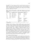
pertinent to the superconductivity of M3C60 (M
=
K,
Rb) is given in Table 1.
In this table:
a0
is
the lattice constant;
T,
is the superconducting transition
temperature;
2A
is the superconducting bandgap;
P
is the pressure;
H,I,
Hc2,
and
H,
are, respectively, the lower critical field, upper critical field,
and thermodynamic critical field;
J,
is the critical current density;
(0
is the
superconducting coherence length;
XL
is the London penetration depth; and
L
is the electron mean free path.
[621.
3
Carbon Nanotnbes
The field
of
carbon nanotube research was launched in 1991 by the initial
experimental observation
of
carbon nanotubes by transmission electron
mi-
croscopy (TEM)
[
1511,
and the subsequent report
of
conditions for the synthe-
sis of large quantities
of
nanotubes [152,153]. Though early work was done on
62
Table
1.
Experimental
values
for
the
macroscopic
parameters
of
the superconducting
phases
of
GC60
and
RbsC60.
Parameter
K3C60
Rb&o
a0
(A)
14.253"
14.436"
19.7'
5.2", 4.0", 3.6g, 3.6h
-7.8'
13j
26j, 301, 29", 17.5'
0.38i
0.12j
2.6j, 3.11,
3.4",
4.5'
240j, 480°, 6OOp,
8OOq
92j
3.1'.
1.0'
-1
.34b,
-3.5'
30.0b
5.3d, 3.1", 3.6f, 3.0g,2.9Sh
-9.7i
263, 19k
34j,
55',
16'
0.44i
1.9
2.0i, 2.0',
3.0"
168j, 370f, 46OP,
8004,
210k
843,
90k
-3.8'
0.9'
aRef.
[27;
'Ref.
[136];
cSTM
measurements in Ref.
[137];
%TM
measurements in
Ref.
[131];
"NMR
measurements in Ref.
[138, 1391;
fpSR
measurements in Ref.
[140];
Var-IR
measurements in
Ref.
[141];
hFar-IR measurements in Ref.
[142];
%Ref
[125];
jRef.
[143];
kReE
[144];
'Ref.
[145];
"Ref.
[146];
nRef.
[147];
ORef.
[148];
PRef.
[138];
qRef.
[129, 1491;
'Ref.
[150];
sRef.
[132].
coaxial carbon cylinders called multi-wall carbon nanotubes, the discovery
of
smaller diameter single-wall carbon nanotubes in
1993
[
154, 1551, one atomic
layer in thickness, greatly stimulated theoretical and experimental interest in
the field. Other breakthroughs occurred with the discovery
of
methods to
synthesize large quantities of single-wall nanotubes with a small distribution
of
diameters
[156,
1571,
thereby enabling experimental observation
of
the
remarkable electronic, vibrational and mechanical properties
of
carbon nan-
otubes. Various experiments carried out thus far
(cg.,
high resolution
TEM,
STM,
resistivity, and Raman scattering) are consistent with identifying single-
wall carbon nanotubes as rolled up seamless cylinders
of
graphene sheets
of
sp2
bonded carbon atoms organized into a honeycomb structure as a flat
graphene sheet. Because
of
their very small diameters (down to
-0.7
nm) and
relatively long lengths (up to
N
several pm), single-wall carbon nanotubes are
prototype hollow cylindrical
1
D
quantum wires.
3.1
Synthesis
The earliest observations of carbon nanotubes with very small (nanometer)
diameters
[151,
158,
1591
are shown in Fig. 14. Here we see results
of
high
resolution transmission electron microscopy
(TEM)
measurements, providing
evidence for pm-long multi-layer carbon nanotubes, with cross-sections show-
ing several concentric coaxial nanotubes and a hollow core. One nanotube has
63
Fig.
14.
High resolution TEM observations
of
three multi-wall carbon nanotubes
with
N
concentric carbon nanotubes with various outer diameters
do
(a)
N
=
5,
do
=
6.7
nm,
(b)
N
=
2,
do
=
5.5
nm, and (c)
N
=
7,
do
=
6.5
nm. The inner
diameter
of
(c) is
d,
=
2.3
nm. Each cylindrical shell is described by its own diameter
and chiral angle
[
1511.
only two coaxial carbon cylinders [Fig. 14(b)], and another has an inner diam-
eter
of
only
2.3
nm [Fig. 14(c)] 11511. These carbon nanotubes were prepared
by a carbon arc process (typical dc current
of
50-100
A
and voltage of
20-
25
V),
where carbon nanotubes form as bundles
of
nanotubes on the negative
electrode, while the positive electrode
is
consumed in the arc discharge in a
helium atmosphere
[160].
The apparatus is similar to that used to synthesize
endohedral fullerenes, except that the metal added to the anode is viewed as a
catalyst keeping the end
of
the
growing
nanotube from closing [156]. Typical
lengths
of
the arc-grown multi-wall nanotubes are ~1 pm, giving rise to an
aspect ratio (length to diameter ratio)
of
lo2
to
lo3.
Because
of
their small
diameter, involving only a small number
of
carbon atoms, and because
of
their large aspect ratio, carbon nanotubes are classified as 1D carbon systems.
Most
of
the theoretical work on carbon nanotubes has been on single-wall
nanotubes and has emphasized their 1D properties.
In
the multi-wall carbon
nanotubes, the measured interlayer distance
is
0.34 nm [151], comparable to
the interlayer separation
of
0.344 nm in turbostratic carbons.
Single-wall nanotubes were first discovered
in
an arc discharge chamber using
a
catalyst, such as Fe,
Co
and other transition metals, during the synthesis
process [154,155]. The catalyst is packed into the hollow core of the electrodes
and the nanotubes condense in a cob-web-like soot sticking to the chamber
walls. Single-wall nanotubes, just like the multi-wall nanotubes and also
conventional vapor grown carbon fibers
[161],
have hollow cores along the
axis of the nanotube.
The diameter distribution
of
single-wall carbon nanotubes
is
of great interest
for both theoretical and experimental reasons, since theoretical studies indi-
cate that the physical properties of carbon nanotubes are strongly dependent
on the nanotube diameter. Early results for the diameter distribution
of
Fe-catalyzed single-wall nanotubes (Fig.
15)
show a diameter range between
0.7
nm and
1.6
nm, with the largest peak in the distribution at
1.05
nm, and
with a smaller peak at 0.85 nm [154]. The smallest reported diameter for a
single-wall carbon nanotube is
0.7
nm [154], the same as the diameter
of
the
C~O molecule
(0.71
nm)
[162].
Two recent breakthroughs in the synthesis of single-wall carbon nanotubes
[156,
1571
have provided a great stimulus to the field by making significant
amounts of available material for experimental studies. Single-wall carbon
nanotubes prepared by the Rice University group by the laser vaporization
method utilize a Co-Nilgraphite composite target operating in a furnace
at 1200°C. High yields with
>70%90%)
conversion of graphite to single-
wall nanotubes have been reported [156,
1631
in the condensing vapor
of
the heated flow tube when the Co-Ni catalystharbon ratio was
1.2
atom
%
Co-Ni alloy with equal amounts
of
Co and Ni added to the graphite
(98.8
atom
%I).
Two sequenced laser pulses separated by a 50 ns delay were used to
65
0.7
OB
0.9
1.0 1.1
1.2
1.3 1.4
1.5 1.6
Nanotube
diameters
(nm)
Fig.
15.
Histogram
of
the
single-wall nanotube diameter distribution for Fe-catalyzed
nanotubes
[154].
A
relatively small range of diameters
are
found, the smallest diameter
corresponding to
that
for the hllerene
(260.
provide
a
more uniform vaporization of the target and to gain better control
of the growth conditions. Flowing argon gas sweeps the entrained nanotubes
from the high temperature zone
to
a water-cooled Cu collector downstream,
just outside the furnace
[156].
Subsequently, an efficient
(>70%1
conversion)
carbon arc method (using a Ni-Y catalyst) was found by a French group at
Montpellier
[157]
for growing single-wall carbon nanotube arrays with a small
distribution
of
nanotube diameters, very similar to those produced by the Rice
group
[156, 1631.
Other groups worldwide are now also making single-wali
carbon nanotube ropes using variants of the laser vaporization or carbon arc
methods.
The nanotube material produced by either the laser vaporization method or
the carbon arc method appears in a scanning electron microscope (SEM)
image as
a
mat
of
carbon “ropes”
10-20
nm in diameter and up to 100 pm or
more in length. Under transmission electron microscope
(TEM)
examination,
each carbon rope is found to consist primarily of a bundle of single-wall
carbon nanotubes aligned along a common axis. X-ray diffraction (which
views many ropes at once) and transmission electron microscopy (which
views a single rope) show that the diameters of the single-wall nanotubes
have a strongly peaked narrow distribution
of
diameters. For the synthesis
conditions used by the Rice and Montpellier groups, the diameter distribution
was strongly peaked at
1.38f0.02 nm, very close to the diameter of an ideal
(1
0,10>
nanotube. X-ray diffraction measurements
[
156,
1
571
showed that
these single-wall nanotubes form a two-dimensional triangular lattice with a
66
lattice constant of
1.7
nm, and an inter-tube separation of
0.3
15
nm at closest
approach within a rope, in good agreement with prior theoretical modeling
results
[164,
1651.
Whereas multi-wall carbon nanotubes require no catalyst for their growth,
either by the laser vaporization or carbon arc methods, catalyst species are
necessary for the growth of the single-wall nanotubes
[156],
while two different
catalyst species seem to be needed to efficiently synthesize arrays
of
single
wall
carbon nanotubes by either the laser vaporization or arc methods. The
detailed mechanisms responsible
for
the growth of carbon nanotubes are not
yet well understood. Variations in the most probable diameter and the width
of
the diameter distribution is sensitively controlled by the composition
of
the
catalyst, the growth temperature and other growth conditions.
3.2
Structure
of
Carbon
Nanotubes
The structure of carbon nanotubes has been explored by high resolution
TEM and STM characterization studies, yielding direct confirmation that the
nanotubes are cylinders derived from the honeycomb lattice (graphene sheet).
Strong evidence that the nanotubes are cylinders and are not scrolls comes
from the observation that the same numbers of walls appear on the left and
right hand sides of thousands of TEN images of nanotubes, such as shown
in Fig.
14.
In pioneering work, Bacon in 1960 [166] synthesized graphite
whiskers which he described as scrolls, using essentially the same condtions as
for the synthesis of carbon nanotubes, except for the use of helium pressures
higher by an order
of
magnitude to synthesize the scrolls. It is believed that
the cross-sectional morphology of multi-wall nanotubes and carbon whisker
scrolls is different.
A
single-wall carbon nanotube is conveniently characterized in terms of its
diameter
dt,
its chiral angle
8
and its
1D
(onsdimensional) unit cell, as shown
in Fig. 16(a). Measurements of the nanotube diameter
dt
and chiral angle
8
are conveniently made by using STM (scanning tunneling microscopy) and
TEM (transmission electron microscopy) techniques. Measurements of the
chiral angle
8
have been made using high resolution TEM [154, 167, and
8
is normally defined by taking
8
=
Oo
and
6'
=
30°,
for zigzag and armchair
nanotubes, respectively. While the ability to measure the diameter
dt
and the
chiral angle
8
of
individual single-wall nanotubes has been demonstrated, it
remains
a
major challenge to determine
dt
and
0
for
specific nanotubes that
are used for an actual physical property measurements, such as resistivity,
Raman scattering, infrared spectra, etc.
The circ_umference
of
any carbon nanotube is expressed in terms of the chiral
vector
ch
=
nfi1
+
mfia
which connects two crystallographically equivalent
sites on
a
2D
graphene sheet [see Fig. 16(a)]
[162].
The construction in
67
-+
Fig. 16.
(a) The chiral vector
OA
or
&
=
niL1
+
miL2
is defined on the honeycomb
lattice of carbon atoms by unit vectors
iL1
and
iL2
of a graphene layer and the
chiral
angle 0 with respect to the zigzag axis
(0
=
0").
Also shown are the lattice vector
OB=
T
of the
1D
nanotube unit cell, the rotation angle
$
a2d the translation
7'.
The lattice vector of the 1D nanotube
T
is determined by
ch.
Therefore the
integers
(n,
m)
uniquely specify the symmetry of the basis vectors of a nanotube. The
basic symmetry operation for the carbon nanotube is
R
5
($I?).
The diagram
is
constructed for (n,
m)
=
(4,2).
(b) Possible chiral vectors
ch
specified by the pairs
of
integers
(n,
m)
for general carbon nanotubes, including zigzag, armchair, and chiral
nanotubes. According to theoretical calculations, the encircled dots denote metallic
nanotubes, while the small dots are for semiconducting nanotubes [162].
-+
68
Fig.
17.
Schematic models for
a
single-wall carbon nanotubes with the nanotube
axis
normal
to:
(a) the
B
=
30”
direction
(an
“armchair”
(n,
n)
nanotube),
(b)
the
0
=
0’
direction
(a
“zigzag”
(n,
0)
nanotube),
and
(c)
a
general direction, such
as
OB
(see
Figure
16),
with
0
<
0
<
30”
(a
“chiral”
(n,
m)
nanotube). The
actual
nanotubes
shown
here
correspond
to
(n,
rn)
values
of:
(a)
(5,5),
(b)
(9,0),
and (c)
(10,5)
[168].
Fig. 16(a) shows the chiral angle
8
between the vector
C?h
and the “zigzag”
direction
(0
=
0),
and
shows the unit vectors
iL1
and
62
of
the hexagonal
honeycomb lattice [Figs. 16(a) and 171. An ensemble
I
of
chiral vectors specified
by pairs
of
integers
(n,
m)
denoting the vector
ch
=
n6l
+
m&
is given in
Fig. 16(b) [169].
The cylinder connecting the two hemispherical caps
of
the carbon nanotube
is formed by superimposing the two ends
of
the vector
C?h
and the cylinder
joint is made along the two lines
OB
and
AB’
in Fig. 16(a). The lines
OB
and
AB’
are both perpendicular to the vector
eh
at each end
of
6h
[162].
The
intersection
of
OB
with the first lattice point determines the fundamental
1D
translation vector
T’
and thus defines the length
of
the unit cell
of
the
1D
lattice [Fig. 16(a)]. The chiral nanotube, thus generated has no distortion
of
bond angles other than distortions caused by the cylindrical curvature
of
the
nanotube. Differences in the chiral angle
B
and in the nanotube diameter
dt
give rise to differences
in
the properties
of
the various graphene nanotubes. In
the
(n,
m)
notation for
(?h
=
n&1
+
miL2,
the vectors
(n,
0)
or
(0,
m)
denote
zigzag nanotubes and the vectors
(n,
n)
denote armchair nanotubes. All other
vectors
(n,
rn)
correspond
to
chiral nanotubes [169]. In terms
of
the integers
(n,
m),
the nanotube diameter
dt
is given by
+
dt
=
&ac-c(m2
+
mn
+
n2)1’2/x
(2)
69
and the chiral angle
8
is given by
e
=
tan-l(J?;n/(2m
+
n)).
(3)
The number of hexagons,
N,
per unit cell of a chiral nanotube is specified by
the integers
(n,
m)
and is given by
2(m2
+
n2
+
nm)
dR
N=
(4)
where
dR
is the greatest common divisor of (2n
+
m,
2m
+
n)
and
is
given by
(5)
d
3d
if
n
-
m
is not
a
multiple
of
3d
if
n
-
m
is
a
multiple
of
3d,
dR=
{
where
d
is
the greatest common divisor of
(n,
m).
The addition of a hexagon
to the structure corresponds to the addition of two carbon atoms.
As
an
example, application of Eq.
(4)
to the
(5,5)
and (9,O) nanotubes yields values
of 10 and
18,
respectively, for
N.
Since the 1D nanotube unit cell in real
space is much larger than the 2D graphene unit cell, the 1D Brillouin zone
is therefore much smaller than the one corresponding to a single 2-atom
graphene unit cell. The application of Brillouin zone-folding techniques has
been commonly used to obtain approximate electron and phonon dispersion
relations for carbon nanotubes with specific symmetry
(n,
m),
as discussed
in
53.3.
Because
of
the special atomic arrangement of the carbon atoms in a carbon
nanotube, substitutional impurities are inhibited by the small size of the
carbon atoms. Furthermore, the screw axis dislocation, the most common
defect found in bulk graphite, is inhibited by the monolayer structure of
the
Cs0
nanotube. For these reasons, we expect relatively few substitutional
or structural impurities in single-wall carbon nanotubes. Multi-wall carbon
nanotubes frequently show “bamboo-like’’ defects associated with the termi-
nation of inner shells, and pentagon-heptagon
(5
-
7)
defects are also found
frequently
[7].
3.3
Electronic Structure
Structurally, carbon nanotubes of small diameter are examples of a one-
dimensional periodic structure along the nanotube axis. In single wall carbon
nanotubes, confinement of the structure in the radial direction is provided by
the monolayer thickness of the nanotube in the radial direction. Circumferen-
tially, the periodic boundary condition applies to the enlarged unit cell that
is
formed in real space. The application of this periodic boundary condition
to the graphene electronic states leads to the prediction of a remarkable
electronic structure for carbon nanotubes of small diameter. We first present
70
3
2
1
eo
2
-1
-2
-3
ki
k
k k
Fig.
18.
One-dimensional energy dispersion relations for
(a)
armchair
(5,5)
nanotubes,
@)
zigzag
(9,O)
nanotubes,
and
(c)
zigzag
(10,O)
nanotubes.
The
energy
bands
with
a
symmetry
are
non-degenerate,
while
the
e-bands
are
doubly
degenerate at
a
general
wave vector
k:
[169,
175,
1761.
a
summary
of
theoretical predictions, followed by
a
summary of experimental
observations which lend support to these predictions.
The
ID
electronic energy bands for carbonnanotubes [170,171, 172,
173,
1741
are related to bands calculated for the
2D
graphene honeycomb sheet used
to
form the nanotube. These calculations show that about 1/3 of the nanotubes
are metallic and
2/3
are semiconducting, depending on the nanotube diameter
dt
and chiral angle
8.
It can be shown that metallic conduction in a
(n,
m)
carbon nanotube is achieved when
2n+m=3q
(6)
where
q
is an integer.
All
armchair carbon nanotubes
(8
=
30")
are metallic
and satisfy
Eq.
(6).
The metallic nanotubes, satisfying
Eq.
(6),
are indicated in
Fig. 16(b) as encircled dots, and the small dots correspond to semiconducting
nanotubes.
Calculated dispersion relations based on these simple considerations are
shown for metallic nanotubes
(n,
m)
=
(5,5)
and
(9,O)
in Figs. 18(a) and
(b), respectively, and for a semiconducting nanotube
(n,
m)
=
(10,O)
in
Fig.
18(c) [175]. Figure 16(b) and
Eq.
(6)
shows that all armchair nanotubes
(n, n)
are metallic, but only
113
of the possible zigzag nanotubes
(n,
0)
and
(0,
m)
are metallic
[169]).
The calculated electronic structure can be either
metallic or semiconducting depending on the choice
of
(n,
m),
although there
is no difference in the local chemical bonding between the carbon atoms in
the nanotubes, and no doping impurities are present [169].
These surprising results can be understood on the basis of the electronic struc-
ture
of
a graphene sheet which is found to be
a
zero gap semiconductor
1177
with bonding and antibonding
7r
bands that are degenerate at the K-point
(zone corner) of the hexagonal
2D
Brillouin zone. The periodic boundary
71
Fig.
19.
The
energy
gap
E,
for
a
general
chiral
single-wall
carbon
nanotube
as
a
function
of
100
&dt,
where
dt
is
the
nanotube
diameter
in
8,
[179].
conditions for the
1D
carbon nanotubes
of
small diameter permit only a
few wave vectors to exist in the circumferential direction and these satisfy
the relation
nX
=
7rdt
where
X
=
2n/k.
Metallic conduction occurs when
one of these wave vectors
k
passes through the K-point
of
the
2D
Brillouin
zone, where the valence and conduction bands are degenerate because
of
the
symmetry
of
the
2D
graphene lattice.
As
the nanotube diameter increases, more wave vectors become allowed for
the circumferential direction, the nanotubes become more two-dimensional
and the semiconducting band gap disappears, as is illustrated in Fig.
19
which
shows the semiconducting band gap to be proportional to the reciprocal
diameter
l/dt.
At
a
nanotube diameter
of
dt
N
3
nm (Fig.
19),
the bandgap
becomes comparable to thermal energies at room temperature, showing that
small diameter nanotubes are needed to observe these quantum effects. Cal-
culation
of
the electronic structure for two concentric nanotubes shows that
pairs
of
concentric metal-semiconductor or semiconductor-metal nanotubes
are stable
[178].
Closely related to the
1D
dispersion relations for the carbon nanotubes
is
the
1D
density
of
states shown in Fig.
20
for:
(a)
a
semiconducting
(10,O)
zigzag
carbon nanotube, and
(b)
a metallic
(9,O)
zigzag carbon nanotube. The results
show that the metallic nanotubes have a small, but non-vanishing
1D
density
of
states, whereas for a
2D
graphene sheet (dashed curve) the density
of
states
72
r_l
1.0
al
c
Ti
u-
0
0)
0
-
0.5
C
- -
2
%
_1
2
oa
0.0
rn
4.0
-3.0
-2.0
-1.0
0.0
1.0
2.0
3.0
Energyly,
0
v)
B
0.0
4.0
-3.0
-2.0
-1.0
0.0
1.0
2.0
3.0
4.0
Energyly,
Fig.
20.
Electronic
1D
density of states per unit cell
of
a
2D
graphene sheet
for
two
(n,
0)
zigzag nanotubes: (a) the
(10,O)
nanotube which has semiconducting behavior,
(b) the
(9,O)
nanotube which has metallic behavior.
Also
shown in the figure
is
the
density of states for the
2D
graphene sheet (dotted line)
[178].
is zero at the Fermi level, and varies linearly with energy, as we move away
from the Fermi level.
In
contrast, the density
of
states for the senliconducting
1D
nanotubes is zero throughout the bandgap, as shown in Fig. 20(a).
From these results, one could imagine designing an electronic shielded wire
device less than
3
nm in diameter, consisting of two concentric graphene
nanotubes with a smaller diameter metallic inner nanotube surrounded by a
larger diameter semiconducting (or insulating) outer nanotube. Such concepts
could in principle be extended to the design
of
tubular metal-semiconductor
all-carbon devices without introducing any doping impurities
[169],
Experimental measurements to test the remarkable theoretical predictions
of
the electronic structure of carbon nanotubes are difficult to carry out because
73
of
the strong dependence of the predicted properties on nanotube diameter
and chirality. The experimental difficulties arise from the great experimental
challenges in making electronic or optical measurements on individual single-
wall nanotubes, and further challenges arise in making such demanding
measurements on individual nanotubes that have been characterized with
regard to diameter and chiral angle
(dt
and
0).
Despite these difficulties,
pioneering work has already been reported on experimental observations
relevant to the electronic structure of individual multi-wall nanotubes, on
bundles of multi-wall nanotubes, on a single bundle or rope of single-wall
carbon nanotubes, and even on an individual single-wall nanotube.
The most promising present technique for carrying out sensitive measure-
ments of the electronic properties of individual nanotubes is scanning tun-
neling spectroscopy (STS) because of the ability
of
the tunneling tip to
sensitively probe the electronic density of states of either
a
single-wall nan-
otube 1180, 1811 or the outermost cylinder of
a
multi-wall nanotube 11821,
because of the exponential dependence of the tunneling current on the dis-
tance between the nanotube and the tunneling tip. With ths technique, it
is
further possible to carry out both STS and scanning tunneling microscopy
(STM) measurements on the same nanotube and therefore to measure the
nanotube diameter concurrently with the
STS
spectrum
[182].
It has also been
demonstrated that the chiral angle
0
of
a
carbon nanotube can be determined
using atomic resolution STM techniques [183, 1811 or high-resolution TEM
[151,!54,184,185,186].
Several
groups
have thus far attempted STS studies
of
individual nanotubes
[186,
182,
18
11. The studies which appear to provide the most detailed test
of
the theory for the electronic properties of 1D carbon nanotubes, thus far, use
the combined
STM/STS
technique [182, 1811. In this early STMlSTS study,
more than nine individual multi-wall nanotubes with diameters ranging from
1.7
to
9.5
nm were examined. Topographic STM measurements were also
made to obtain the maximum height of the nanotube relative to the gold
substrate. thus determining the diameter of an individual nanotube [182].
Then switching to the
STS
mode
of
operation, current-voltage (I-V) plots
were made on the same region
of
the same nanotube as was characterized
for its diameter by the STM measurement. The
I-V
plots for three typical
nanotubes are shown in Fig.
21.
The results on this figure provide evidence
for
one metallic nanotube with
dt
=
8.7
nm [trace (I)] showing ohmic behavior,
and two semiconducting nanotubes [trace (2) for a nanotube with
dt
=
4.0 nrn
and trace
(3)
for a nanotube with
dt
1.7
nm] showing plateaus
at
zero
current and passing through
V
=
0.
The
dI/dV
plot
in the upper inset
provides
a
tunneling density of states measurement for carbon nanotubes, the
peaks in the
dI/dV
plot being attributed to singularities in the 1D density of
states, as are shown in Fig. 20. Similar studies on single-wall nanotubes under
higher resolution conditions show much more clearly defined density
of
states
74
40
t
.
.
. .
.
.
.,
. .
.
.
. .
. . .
,
.
. .
.~~FrI.
*
I
*
.
.
.
. .
.
.
q
Fig.
21.
Current-voltage
I
vs.
V
traces taken with scanning tunneling spectroscopy
(STS)
on individual nanotubes
of
various outer diameters:
(1)
dt
=
8.7
nm,
(2)
dt
=
4.0
nm, and
(3)
&
=
1.7
nm.
The top inset shows the conductance
vx
voltage
plot for
data
taken on
the
1.7
nm nanotube. The bottom inset shows an
I-V
trace
taken
on
a gold surface under the same conditions
[
1821.