SMT Soldering Handbook surface mount technology 2nd phần 5 potx
Bạn đang xem bản rút gọn của tài liệu. Xem và tải ngay bản đầy đủ của tài liệu tại đây (2.73 MB, 37 trang )
job:LAY04 page:49 colour:1 black–text
demand a solder with a different melting point or maybe a certain percentage of
silver, the user will be well advised never to change the specification of his
solder. The upheaval which would be caused by changing from the standard
tin–lead solder to a lead-free one (Section 3.2.3) explains the general reluctance
of the industry to adopt a lead-free technology, unless forced to do so.
4. The standard wavesoldering temperature of 250 °C/480 °F plus or minus a few
degrees is, like the conveyor angle, the result of over four decades of practical
wavesoldering experience. Without a compelling need, it is advisable not to
depart from it.
4.7.2 Choosing and monitoring operating parameters
Condition of the flux
Given that the choice of flux is settled, the contents of the fluxer should at all times
match the density and/or the acid value which is specified in the vendor’s data sheet.
Section 4.2.2 discusses in detail how this requirement can be met, by automatic
equipment if required. It is worth restating at this point that the success of
wavesoldering depends critically on the consistent quality of the flux, and that this
constancy is assured more easily with sprayfluxers than with foamfluxers.
Amount of flux per unit of board area
This parameter also affects the soldering success, though to a lesser degree than the
density and the activity of the flux. Too much flux means more solvent in the flux
cover and, unless the preheater is adjusted accordingly, a risk of boiling and
solder-prill formation as the board passes through the solderwave. If boards have to
be cleaned after soldering, too much flux reduces the cleaning efficiency. Too little
flux, uneven fluxcover or, worse, unfluxed patches inevitably cause soldering faults,
such as bridges, icicles, solder adhering to the board and open joints, especially with
low-solids fluxes. With these, the margin of error is much narrower than with
high-solids fluxes.
The thickness of the flux cover can be controlled to some extent with the various
types of sprayfluxer, but foamfluxers permit very little, if any, control over this
parameter. At the time of writing (1997), there is no equipment on the market for
automatically monitoring the thickness of the flux cover. A frequent visual check of
the overall appearance of the soldered boards is the best method of ensuring the
stability of this important factor. Automatic video surveillance of the output of a
soldering line should be capable of giving warning of a malfunction of the fluxing
unit.
Intensity of preheating
Insufficient preheat leaves too much solvent in the fluxcover, which is therefore
more liable to be washed off in the solderwave, leading to bridging or open joints.
This factor is particularly critical with double waves, where a substantial portion of
Wavesoldering 131
job:LAY04 page:50 colour:1 black–text
the flux cover must survive the passage through the first, turbulent wave. Moreover,
if the board is too cool, the solder may not rise through all plated holes and form the
required solder meniscus on the upper board surface.
Too sharp a preheat can cause trouble with rosin-based fluxes: overbaking such a
flux will cause the rosin to polymerize. This reduces its mobility, so that it may
obstruct the solder in tinning all solderpads or in rising to the top surface of the
board. It will certainly make cleaning less efficient.
By contrast, fluxes with a low solids content and very little rosin, and the
so-called ‘no-clean’ fluxes (Sections 3.5 and 8.1) which are mostly rosin-free,
require more intense preheating to ensure that the flux coating is not washed off in
the double solderwave. With these fluxes, most vendors suggest that the underside
of the board should have a temperature of 120 °C/250 °F on emerging from the
preheating stage.
The methods of controlling the intensity of preheating are dealt with in Section
4.2.3.
Parameters of the solderbath and the wave
The level of molten solder in the machine should at all times be kept strictly at the
height recommended by the maker. Many machines are fitted with an automatic
solder feeder, which maintains the correct solder level. Failing an automatic level
control, the solder level must be regularly checked at intervals depending on the
usage of the machine, and if necessary topped up. Unless fitted by the maker, it is
advisable to install a simple solder-level sensor, which gives an audible or visible
warning as soon as the solder level drops below the maker’s danger mark.
If the solder level drops too low, dross and flux-residues which float on the
solderbath can be sucked into the inlet of the solderpump. Once in the solder
stream, they tend to deposit on the solder conduits and the pump impeller. These
deposits interfere with the steady running of the solderwave, as will be discussed
below. Particles of dross and flux which reach the wave nozzle emerge in the wave
as small, but conspicuous, black spots, which pop up in the wavecrest and finish up
on the surface of the solderjoints. Such dross or flux inclusions do not necessarily
threaten the function or reliability of the affected joints, but they are a legitimate
cause of rejection by quality control or by the customer.
The temperature of the solder is one of the most basic wavesoldering parameters.
The general suitability of 250 °C/480 °F for most wavesoldering tasks has been
mentioned already. Close adherence to this value is less critical than is often
assumed, an accuracy of ±2–3 °C/4–6 °F being quite sufficient. It is much more
important to guard against a slow, unnoticed upward or downward drift of the
solder temperature away from its set value. The temperature readout on the control
panel of the machine, together with its warning signals, may be misleading: software
or functional errors are not unknown. The safest way to guard against this danger is
to check the actual solder temperature halfway through every working shift by
checking it with a reliable, preferably occasionally re-calibrated, handheld tempera-
ture measuring instrument, with its sensor placed in the solderwave about 5–
10 mm/0.25–0.5 in below the crest.
132 Wavesoldering
job:LAY04 page:51 colour:1 black–text
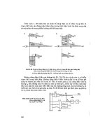
Figure 4.30
Checking the wave height.
: Conveyor angle
The height of a wavecrest is directly linked to the speed of the solder pump,
which with most good machines has a slip-free, tachometrically controlled drive
which is protected against variations in the supply voltage. The waveheight and its
consistency across the whole width of the wave can be checked very simply by
sliding a piece of plain FR4, with gradations marked on it, across the length of the
wavenozzle while the pump is running (Figure 4.30). It is advisable to carry out this
simple check at the beginning of every shift. Some computer-controlled machines
are fitted with a sensor-operated surveillance of the height and integrity of their
solderwave(s).
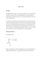
The depth of immersion of a board into the crest of the solderwave is normally
equivalent to the thickness of the board. It is therefore important that the underside
of the board is strictly parallel to the line of the wavecrest to well within this
measure. This is easily checked by letting a piece of plain FR4 without copper
lamination, as wide as the largest board, run across the wave and stop briefly over the
wavecrest. The flattened wavecrest will be clearly visible through the translucent
FR4. If the board is parallel to the wavecrest, the width of the band formed by the
flattened wave will be the same across the whole breadth of the testboard (Figure
4.31).
If the board is not parallel to the wavecrest, the whole conveyor must be tilted
sideways until a parallel position is achieved. Provisions for carrying out this
adjustment are, or should be, a feature of every wavesoldering machine. As an
alternative to the FR4 board, many machine vendors can supply a plate of heat-
resistant borosilicate glass which carries a pattern of parallel lines to make it easy to
check the width of the wavecrest across the plate. To make sure that the glass plate
does not crack during this manoeuvre, it is advisable to pass it over the fluxer and the
preheater before arresting it over the wave. With FR4, this is not necessary.
Uneven or rough running of the solderwave, such as fluttering of the
Wavesoldering 133
job:LAY04 page:52 colour:1 black–text
Figure 4.31
Checking depth of immersion and horizontal alignment between
wavecrest and board
waveheight, can be a sign that deposits of dross or flux residues have formed on the
pump impeller or the solder ducts, often as a consequence of an unduly low solder
level in the machine (see above). With all jetwaves, even quite small accretions of
dross or flux residue in the exit slot of the wavenozzle can ruin the smooth profile of
the solderjet. The wavecrest becomes ragged. One big dross particle can depress it
by quite large amounts, naturally leading to serious soldering defects. Regular
cleaning of the nozzle aperture is an important requirement with all jetwaves. It is
best carried out by drawing a scraping tool, made from soft steel or PTFE, along the
whole length of the nozzle aperture. Most vendors can supply suitable implements
for the purpose. A scraper made from aluminium, brass, copper or hardened steel
should on no account be used.
With all double-wave machines, the second wave is of the ‘asymmetrical’ type
(see Section 4.4.4). On the exit side of this kind of wave, the board lifts off from a
horizontal pool of solder, whose surface moves in the same direction and ideally at
the same speed as the board on its conveyor for reasons which have been explained
already (see Figure 4.14). The match between these two speeds can be checked
simply by floating a small steel ball, for instance from a ball bearing, on the solder
surface and comparing its movement with that of the board conveyor.
134 Wavesoldering
job:LAY04 page:53 colour:1 black–text
Conveyor speed
The conveyor speed is a critical wavesoldering parameter. On the one hand, the
heat received by a board is inversely proportional to the speed at which it travels
through the preheating unit at a given setting of the heater panels. On the other
hand, the maximum practicable soldering speed of a wave machine is governed
not only by the ability of the solderwave to get the necessary amount of heat into
the board within the time available for this, but also by the complexity of its
pattern and the density of its population of components. Furthermore, multilayer
boards with high heat capacity must travel more slowly than simple single-layer
boards. Boards with closely set SMDs and fine-pitch multilead components must
travel over the wave more slowly to give the solder a chance to flow into the
narrow gaps between neighbouring components, and to drain away from the fine
pattern of leads.
With most soldering machines, the set and the actual conveyor speed are
displayed on the control panel. Nevertheless, it should be part of the machine-
minder’s task to check the actual against the displayed conveyor speed of the
machine once every day, with the aid of a stopwatch and a simple marker, travel-
ling on the chain conveyor over a measured distance marked on the conveyor
rail. This very simple test can save hours of expensive rework of boards, should the
conveyor speed have drifted from its set value, or should the machine control
have started to malfunction.
Computer-controlled soldering machines
The large number of interlinked operational parameters makes wavesoldering a
natural subject for computer control, which generally has two tasks.
The first task is the monitoring and stabilizing of all parameters, which will have
been established as optimal and stored in the program. It is worth saying again that
this automatic pilot does not relieve the operating personnel from periodically
verifying that the machine does in fact run correctly. The functions which must be
watched are those which are difficult if not impossible to monitor by sensors, such as
the behaviour of the foamwave, the spraypattern of the fluxer and the correct
behaviour of the solderwave.
The second task relates to parameters which can be adjusted to suit a given type of
circuit board. The main parameter here is the conveyor speed, which can be raised
with boards of simple pattern and modest thermal requirements, or which may need
lowering for complex or multilayer boards. Linked to this is the intensity of preheat.
Low-temperature emitters respond slowly to a change in heater current (see Section
4.3.2), and this factor must be considered in the program. Alternatively, the
inclusion of one or more high-temperature emitters in the preheating unit will
permit a much faster response to the commands of the computer. Some types of
machine allow for a choice between foamfluxing and sprayfluxing to suit different
types of board.
With computer-controlled soldering lines, each board normally carries a barcode
which calls up the correct parameter as it enters the machine. Nevertheless, it is not
Wavesoldering 135
job:LAY04 page:54 colour:1 black–text
at all advisable to run a soldering line with a random mix of different types of board.
It is advisable to gather them in as large batches as possible.
4.7.3 Optimizing machine parameters
The following strategy for starting up a new machine, or changing to a new type of
board, has proved its worth in practice:
1. Check that the conveyor angle is near 7°, and that the conveyor is laterally
horizontal. Place a plain piece of FR4, of the same thickness and size as the
boards to be soldered, in a board carrier or into the chain conveyor and move it
forward into the fluxer. With a foamfluxer, adjust the air pressure so that the
wave can hold the required height with a good margin. With a sprayfluxer, set
the width of the spraypattern to suit the width of the board.
2. Move the board forward to the solderwave. With double-wave machines, set
the primary wave, whether it is of the turbulent type or a jetwave, as high as is
possible without causing the solder to push through apertures in the board and
flood the top surface. With a jetwave of the type where the solder flows in the
direction of the travelling board, make sure that the baffle at the trailing edge of
the board fixture is high enough to prevent the solder from flooding the top of
the board as it leaves the wave. Single jetwaves of the counterflow type need a
safety baffle at the leading edge of the board. Again, set the wave as high as is
possible without flooding the board.
The secondary wave is always of the asymmetrical laminar type. The board is
moved forward so that its leading edge is just in front of the wavecrest. Adjust
the waveheight so that the crest comes approximately level with the top surface
of the board. This means that thicker multilayer boards dip deeper into the
wave, spend more time in contact with it, and in consequence receive more
heat.
Having done this, move the board forward into the wave and check whether
the board is parallel with the wavecrest, as shown in Figure 4.31. If you find that
the board is not parallel with the wavecrest, do not try to adjust the setting of
the whole solderbath or of the wavenozzle, but tilt the conveyor, as has been
described already.
3. Next, set the conveyor speed at half the value which the vendor gives as its
maximum speed, unless operational requirements make it necessary to work
faster than that. It is worth remembering that it is a fact of life in engineering
that the failure-rate or fault-rate of any given equipment or process begins to
rise exponentially as it is driven at a rate or speed approaching its designed
maximum. (Compare the number of pit stops during an Indianapolis race with
the service requirements of a family car.)
Run a board of the pattern which is to be soldered on the machine, without
components, through the fluxer and the preheating stage and check its tem-
perature on leaving the latter (Section 4.3.4). If it gets too hot, reduce the
setting of the heaters. If on the other hand the heater, even at its maximum
setting, does not get the underside of a heavy multilayer board hot enough, fita
136 Wavesoldering
job:LAY04 page:55 colour:1 black–text
top reflector to the preheater if none is provided. If the board is still too cool,
reduce the distance between the heaters and the conveyor. Only if all else fails
(and in this case the design of the machine must be at fault) lower the transport
speed or, better, modify the heating stage yourself.
4. Having balanced the setting of the heating stage and the conveyor speed against
each other, proceed to solder about ten fully assembled boards, and check the
soldering quality of each carefully. If this is satisfactory, enter the set of working
parameters into the machine computer or your production control manual. If
faults persist in an erratic pattern, check the stability of the fluxer and wave
setting; as a last resort, lower the conveyor speed and reduce the setting of the
heating stage accordingly. If faults persist systematically with one or more given
components, check their solderability or the suitability of the layout. For details
of the systematic analysis, interpretation and elimination of soldering faults and
defects, see Chapter 9.
4.7.4 Machine maintenance
Daily
Clean the wavenozzle at the end of the shift, and if necessary also at the mid-shift
break. Turn on the solderpump and check whether the wavecrest is level and stable.
If you are not satisfied, switch off the pump and scrape the inner walls of the solder
conduit with an annealed hacksaw blade. An annealed hacksaw blade will not snap
and constitute a potential danger, nor will it damage the conduit. Restart the
solderpump and skim dross and flux residues, which may now be flushed through
the wavenozzle, from the solderbath. This maintenance is especially important with
jet nozzles.
At the end of the day, clean splashes of solder and flux from the top of the
machine and the rims of the solderbath. With endless-chain conveyors, check the
condition and functioning of the automatic chain cleaners. With board carriages,
remove excessive flux buildup from the holding jaws.
This schedule can be greatly relaxed with soldering units which work under a
nitrogen atmosphere (Section 4.5.2).
Monthly
Lift the wavenozzle assembly and the pump impeller from the solderbath and
remove all adhering dross and flux residue. With foamfluxers, renew the air filter
and clean the foaming stone. With sprayfluxers, clean spraynozzles, if any, and
remove buildup of dried flux, if any. Renew flux in fluxer, unless in the case of a
foamfluxer the scheduled flux renewal has taken place earlier. Clean the exhaust
system of the fluxing unit. Clean and, if necessary, renew air filters.
Annually
Carry out a complete overhaul of the soldering machine. Check all board carriages,
if any, for correct setting and alignment.
Wavesoldering 137
job:LAY04 page:56 colour:1 black–text
Figure 4.32
Taking a solder sample
This schedule applies for soldering lines which are in constant use. With machines
which are used only sporadically the schedule will, of course, be stretched accord-
ingly.
4.7.5 Check-analysis of the solderbath
Depending on the utilization of the machine, the solderbath should be checked at
least once a year for its tin content and its impurity levels. Most solder vendors are
able to carry out this analysis for their customers. Unless your own organization
maintains a central analytical laboratory, and sometimes even then, it is better and
quicker to employ the services of an outside specialist. For the interpretation of the
analytical report, and the measures to be taken if it is unsatisfactory, see Section
3.3.3.
An analytical laboratory requires a sample of solder weighing 100–200 g/3–6 oz,
in the form of a small ingot. In order for this sample to be meaningful and
representative of the contents of the solderbath, the following sampling procedure
should be followed. The wave is switched on and kept running for 1–2 minutes.
The sample is then taken from the over-run of the wave with a small stainless steel
ladle, which must be absolutely dry. This is best assured by preheating it in a
blowflame. The sample is then poured into a simple mould fabricated from heavy
steel or stainless steel sheet, as sketched in Figure 4.32. This mould too must be
absolutely dry, but it ought not to be too hot because the sample should solidify
reasonably quickly.
4.7.6 Dealing with dross
The nature of dross and the manner of its formation are discussed in Section 4.4.5.
The layer of dross which forms on the surface of the solderbath (unless the machine
is run under nitrogen) must be removed periodically to prevent it from being
sucked into the pump inlet. Skimming the dross twice daily is sufficient for this
138 Wavesoldering
job:LAY04 page:57 colour:1 black–text
purpose (Section 4.4.5). The simplest and best method is to gather the dross into
one corner of the bath surface with a simple stainless steel implement, and then to lift
the lump of dross out of the bath with a flat stainless steel spatula such as is obtainable
in any hardware shop. Tilting the spatula after lifting the dross allows most of the
clean solder trapped in it to drain back into the bath. The rest is then put into a steel
container which is provided with a lid. Most solder vendors are prepared to take
back solder dross from their customers once a sufficient quantity has accumulated,
and will credit them for a portion of the clean solder contained in it. Depending on
the circumstances, it may be advisable to demand an analysis of the returned dross
for its metal content from the solder vendor. Compact, fully enclosed electrically
heated melting pots for the in-house recovery of solder from dross are offered by
some equipment vendors.
Skimming the dross from the solderbath twice a day should be enough. Frequent
skimming in order to make the solderbath look attractive, and maybe to impress
visitors or the management, is not only unnecessary but also increases the amount of
dross which forms on the machine. An existing layer of dross helps to protect the
bath from further oxidation.
4.7.7 Hygiene and safety
Lead and its toxic nature
Solder contains about 40% lead, and lead is toxic. However, if treated and handled
with common sense, there need be no danger to any person working with solder in
any of its many forms, such as solderwire, solder ingots, molten solder or solder
paste, provided a few basic facts are recognized.
Lead can be absorbed into the human body only through the digestive system,
while skin contact is harmless. Put crudely, the basic rule is therefore ‘Do not eat
lead, in any of its forms.’ In practice, this means strict observation of a number of
simple rules.
Don’t smoke, eat or consume drinks on the job. Having handled solder or dross,
wash hands thoroughly before smoking, eating or drinking. The reasons for these
rules are obvious: handling a cigarette or food with solder-contaminated fingers
carries the danger of ingesting lead-containing solder. Even small amounts matter,
because lead is a cumulative poison which is not excreted by the normal bodily
functions. Quite apart from that, soft drinks should not under any circumstances be
consumed near any part of an electronic assembly line. Fruit juices and fruit sugar
form reaction products on metallic surfaces which severely affect solderability, and
which are difficult to remove. Aerosol, formed for example by a fizzy soft drink, can
be fatal for the solderability of a circuit board.
An often neglected danger point is the habit of chewing fingernails. The spaces
under the fingernails are notorious collectors of dirt and dust, picked up from
everything that is being handled or touched (as any forensic scientist knows).
Habitual nailbiters should therefore on no account be given jobs which involve the
handling of solder in any of its forms.
Dross must be handled with caution and common sense: it contains a proportion
Wavesoldering 139
job:LAY04 page:58 colour:1 black–text
of powdery lead oxide, which is more dangerous than metallic lead because it is
absorbed more readily into the digestive system. Hence the rule of placing dross
skimmings into a metal container which is fitted with a lid. Dross must be handled
gently, so that it does not form a cloud of dust. It is a sensible precaution to issue a
dust mask to all operators who have to handle dross in larger quantities. On the
other hand, there is no reason for wearing a dust mask when skimming dross from a
soldering machine, because in this form the oxide is trapped within the bulk of the
metal and its adhering flux residues.
Handling molten solder
Molten solder is quite hot and must be treated with respect. The main danger when
handling it arises from the fact that it will spit and splatter violently when it comes in
contact with a wet or even slightly damp surface. This spitting is caused by the
explosive evaporation of any surface moisture trapped under the molten metal.
Hence the strict rule, already mentioned, that every implement which comes into
contact with molten solder must be meticulously dried by preheating. By contrast,
small amounts of liquid spilled onto the surface of molten solder will hiss away
quietly without spitting.
Drops of molten solder on the skin can be painful, and cause small but relatively
harmless local burns. To stop the pain quickly, touch a cold metal surface, or run
cold water onto the burn. Never apply oil or grease, which will only make matters
worse. Application of a small amount of burn-ointment, which normally contains
picric acid, stops the pain, promotes quick healing and prevents blistering. It is
useful to keep a tube or tin of it handy near any machine or bench where molten
solder is handled.
On the other hand, even a minute drop of molten solder which reaches the eye
can fatally damage sight. It is therefore important to issue all operators who have to
handle molten solder, for example when taking a sample of solder from the
solderwave or when emptying a solderpot, with safety goggles. There is, however,
no need to wear goggles when removing the safety screen to watch a board passing
over the solderwave, or when skimming a solderpot (provided the skimming tool is
dry).
Wearing protective gloves is a wise precaution when sampling the solder or
cleaning the wavenozzle. When handling larger amounts of molten solder, such as
when emptying a solderpot, it is advisable to wear an apron or protective clothing.
Solderdrops clinging to clothing are easily removed by touching them with a small
soldering iron set at a low soldering temperature, provided the material is entirely
of natural fibre such as wool, cotton or linen. With synthetic fibres, this method
would not work, and scraping or plucking the solder off is the only way.
When faced with the task of handling larger amounts of molten solder, it is best to
plan one’s strategy in advance: decide what you want to do, and how best to do it,
before you start. Have all implements and receptacles dry and ready in their proper
places. Do not hurry, and move slowly and with deliberation.
140 Wavesoldering
job:LAY04 page:59 colour:1 black–text
4.8 The role of adhesives in wavesoldering
SMDs must be anchored to the board before they are wavesoldered because they
have no leadwires or legs with which to hang on to the substrate. Adhesive joints
have been found to provide the best answer to the problem. Their mechanical
properties are adequate for the task, and they can be broken without undue force if
necessary.
4.8.1 Demands on the adhesive and the glued joint
The glued joint must be strong enough to hold the component securely to the board
during any handling operation which may precede the soldering process, for
example the insertion of wired components with a ‘mixed’ board, and above all
during the wavesoldering procedure itself. These mechanical loads are only modest,
at most of a magnitude of a few newtons. It is important, however, that the joint
does not distort or disintegrate under the influence of the flux solvents during the
preheating stage, and especially during the passage through one or two solderwaves.
Should the removal of a glued and soldered component become necessary
because on inspection it has been found to be faulty or wrongly placed (Section
10.2), the joint should be capable of being broken without undue force and
consequent damage to the substrate (Section 4.8.5). Finally, during the life of the
assembly, the glued joints should not give off or leak any substance, particularly not
one of an ionic nature, which could lower the surface resistance of the board or
interfere with the function of the assembly.
4.8.2 Storage and handling behaviour of adhesives
Adhesives for SMDs are of the reactive, single-component epoxy or acrylic type.
Solvent-containing adhesives and two-component reactive adhesives, which re-
quire mixing before use, are unsuitable for industrial SMD wavesoldering.
Single-component adhesives are a mixture of two ingredients, a polymer-resin
and a hardener, which are capable of reacting with one another, forming a rigid
structure of crosslinked molecules. This reaction requires a trigger to set it off,
which may be a rise in temperature, or exposure to light in the visible or the UV
range, or both these triggering agents, acting simultaneously or in sequence.
A good SMD adhesive must satisfy a number of specific requirements:
1. During storage, resin and hardener should not of course react with one another.
With some adhesives, this may require storage in a refrigerator at about
5 °C/40 °F, to ensure a storage life of up to one year, which is what the
industrial user expects. With many modern adhesives, refrigeration is no longer
necessary, and storage times of up to one year at room temperature (say
25 °C/78 °F) are not unusual.
2. Adropofadhesive,asdispensedontotheboard, may havetobridgea gap between
0.01 mm/0.4 mil and 0.3 mm/12 mil in height (the standoff height of the
component)while,dependingonthe geometry of the layout, its base may haveto
Wavesoldering 141
job:LAY04 page:60 colour:1 black–text
Figure 4.33
Demands on the adhesive spot
fit into a very narrow gap between two footprints (about 1 mm/40 mil with a
micromelf) (Figure 4.33). As a general rule, the dot as put down on the board
shouldbeabout0.05 mm/2 milhigherthanthe standoff height of thecomponent
which it hasto hold down. This requires the dispensed adhesiveto retain its shape
without sagging or ‘slumping’. Any sideways spread of the dispensed drop would
not only lower its height, so that it might fail to contact and hold the component,
but it could also spread over the adjacent solderpads, totally and possibly
irreparably ruining their solderability,and thus the whole circuit board. The type
of behaviour in whichsemiliquidsubstance retains its shape is called ‘thixotropy’.
For similar reasons, the solder pastes which are used in reflowsoldering must also
exhibit thixotropy, which is discussed fully in Section 5.2.1.
Apart from a sideways slump of the adhesive drop, it would be equally fatal
should one of the more mobile constituents of the adhesive leak out sideways
from the drop and contaminate an adjacent solderpad. Finally, the adhesive
must separate neatly from the dispensing nozzle or placement pin, without
forming a tail or thread which might tip over and fall on a solderpad.
The flow behaviour of an adhesive is necessarily temperature dependent,
making it more mobile at highter temperatures. Most manufacturers have
succeeded in reducing this temperature dependence to a minimum. However,
since a very precise dosage of the dispensed adhesive drop is of the essence,
especially with very small melfs and chips, the dispensing ampoules on some
placement systems are heated to a standard temperature.
As a rule, the adhesive does not sit directly on the FR4 of the board, but on
the solder resist. This places certain demands on the adhesion and the surface
properties of the latter which are discussed in Section 6.1.
Very often one or more conductors will pass between the solder pads of a
142 Wavesoldering
job:LAY04 page:61 colour:1 black–text
component. It is important that these conductor tracks are not covered with a
layer of solder, as might be the case with boards made by a ‘subtractive’ process.
If they are, the solder will melt underneath the solder resist as the board passes
through the solderwave. Because the solder resist starts to crinkle as the solder
on which it sits melts, the result is called the ‘orange peel effect’. An SMD glued
to the solder resist loses its safe anchorage when the solder underneath the resist
melts, so that it is in danger of being washed off in the wave. For this reason,
boards for wavesoldering SMDs should preferably be of the ‘solder mask over
bare copper’ or ‘SMOBC’ type (see Section 6.1).
3. After an SMD has been placed on its adhesive dot, it must stick to it strongly
enough to prevent it from shifting its position or falling off, while the board is
handled between the placement of the components and the curing of the glued
joints. This holding power of the uncured adhesive is called ‘green strength’.
Furthermore, an adhesive must be able to maintain its thixotropic behaviour
and its green strength for at least 24 hours between being taken from its
container, or discharged from its dispenser, and its being hardened or cured
prior to soldering (open time).
4. Last, but not least, the adhesive should have a distinctive and conspicuous,
perhaps luminous, colour, so that missing or misplaced dots are easily spotted.
Orange or bright red seem to be the preferred shades.
4.8.3 Applying the adhesive
The precision of both the placement coordinates and the size of every individual dot
of adhesive are critically important, especially with small melfs and chips: a mis-
placed dot, or one which is too large and becomes squeezed out during placement,
is liable to cover a solderpad and make it unsolderable. Removing cured adhesive
from a pad surface is one of the most costly and hazardous operations in corrective
soldering (Section 10.1.1). On the other hand, a dot of insufficient height may not
connect with the component it is supposed to hold.
In most situations adhesive dots have to be of varying height, for reasons
explained above. There are several alternative methods to achieve this:
Sequential application of single dots
Dispensing the adhesives from the nozzle of a cartridge or ampoule is widely
practised. Most vendors offer adhesives in air-pressure operated ampoules, which
can discharge the content in a controllable manner. For manual placement, the
pressure impulse in the hand-held ampoule is controlled by the operator through a
footpedal or a press-button. The operation is simple, and misplaced adhesive can be
wiped off, with solvents supplied by most vendors.
Dispensing adhesive from ampoules can be mechanized in two ways:
1. For putting down dots of adhesive onto boards before the components are
placed, automatic equipment, which is capable of being programmed, is on the
market. With these machines, the dispensing ampoule is mounted on an xy
Wavesoldering 143
job:LAY04 page:62 colour:1 black–text
Figure 4.34
Dispensing gantry
movable gantry (Figure 4.34). The precision and repeatability of dosage and
placement are of a high enough order to meet the requirements of adhesive
application to modern, closely populated boards.
The distance between the nozzle tip and the board can be varied and
programmed, not only to suit the size of individual dots, but also to enable two
dots to be placed on top of one another (piggy-back) to cater for exceptionally
high standoffs. A ‘suck-back’ at the end of a delivery impulse prevents the
formation of a dangerous string of glue when the nozzle is lifted off. The
dispensing program can be derived from the software of the board layout. The
speed is limited by the various manoeuvres which have to be performed
between discharges, such as starting and stopping the dispensing head, adjusting
its position in the vertical z axis, actuating the displacement mechanism, and
executing the ‘suck-back’. Within these limitations, vendors claim maximum
achievable dispensing rates of up to 17 000 dots/hour, i.e. over 4 dots/second.
Another technique for putting down individual, metered amounts of adhes-
ive is derived from ink-jet printing. The duration of an individual discharge is as
short as 0.001 seconds, which makes it possible to use ‘on-the-fly’ dispensing,
where the dispensing head does not stop moving. Thus, dispensing speeds of 20
dots/sec, i.e. 72 000 dots/hour, are possible. Jet dispensing units can be integ-
rated in-line with high-speed pick-and-place equipment. The major adhesive
vendors are able to supply adhesives suitable for jet-dispensing.
2. Many automatic sequential pick-and-place machines are or can be fitted with
an adhesive dispensing station, which puts down measured dots of adhesive and
precedes the component placement station. The dispensing details are the same
as with the dispensing gantry. With simultaneous pick-and-place machines, the
adhesive is often placed directly on the underside of each component in the
time interval between pickup and placement (see Section 7.3.2).
Stencilprinting the adhesive
Some major vendors offer equipment and adhesives, which by using specially
developed plastic stencils, and by controlling the thixotropic behaviour of the
144 Wavesoldering
job:LAY04 page:63 colour:1 black–text
Figure 4.35
Hardening curve of an epoxy adhesive
adhesive, permit the print-down of adhesive dots of varying and controllable height
on to a board in one single printing operation. By choosing the right aperture
diameter, dots varying in height from 0.125 mm/5 mil to 1 mm/40 mil can be
printed with a 0.3 mm/12 mil thick stencil onto a given board in one pass. Also, dots
do not necessarily have to be round, but may be given other outlines if required.
The advantages are obvious: apart from speeding up the process, parameters of the
adhesive such as a tendency to form strings are no longer critical. Vendors of the
printing equipment claim printdown rates of up to 14 4000 dots per hour.
4.8.4 Curing the adhesive joint
After all components have been placed on the ‘green’ adhesive, the joints must be
cured. Curing transforms the adhesive from a viscous mass into a firm, solid body.
This is achieved by triggering a reaction between the two constituents of the
adhesive, which crosslinks the individual mobile polymer molecules of the resin
constituent into a coherent, semicrystalline mass. It is important that the joint does
not shrink or crack during curing.
With most epoxy and acrylic adhesives, heat provides the required trigger. As is
natural with any chemical reaction, the higher the temperature, the shorter the time
in which the crosslinking reaction proceeds throughout the joint (Figure 4.35).
With a modern adhesive, all joints on a board are sufficiently hard for wavesoldering
after two to three minutes at a curing temperature of 120 °C/250 °F.
Curing can be carried out in an infrared oven, similar to or identical with a
reflowsoldering oven (Section 5.4.4). It must be remembered, however, that with
Wavesoldering 145
job:LAY04 page:64 colour:1 black–text
Figure 4.36
Location of adhesive spots for ultraviolet hardening
the exception of small melfs and chips, the adhesive joint is shielded from the
radiation by the sometimes large and thick component. For adhesive curing,
therefore, an efficient convection oven is best. There is no advantage in carrying out
this curing operation in a nitrogen atmosphere.
As an alternative to heating, or possibly in addition, exposure of the adhesive to
ultraviolet light is also effective in promoting the curing process. This mechanism
will only work if the adhesive, or at least some of it, is ‘visible’ to the light source and
not covered by the component (Figure 4.36). Simultaneous exposure to heat and
light can shorten the curing time by up to 50 per cent.
A type of adhesive is available which contains a light-sensitive initiator. This has
the effect of adding a ‘hairtrigger’ mechanism to the crosslinking reaction: exposure
of the dots of adhesive to a dose of visible light for one-half to four minutes
(depending on the intensity of the light source), before the components are placed,
firms up the adhesive and increases its green strength without starting the crosslink-
ing proper. Once the components are placed, which must be done within 30
minutes after the light exposure, full curing of the joints can be completed in a much
shorter time or at a much lower temperature than is the case with conventional
adhesives.
4.8.5 The glass transition temperature
No assembly process is entirely free from faults, and occasionally glued and wavesol-
dered components must be removed from a board. However, while soldered joints
can be unsoldered, a glued joint cannot be ‘unglued’ but must be broken. The
so-called ‘glass transition’ mechanism of crosslinked polymers makes it possible to
break cured joints without damaging the board. Above a certain temperature,
which is called the glass-transition temperature (T
%
) the crosslinked bonds between
neighbouring molecules begin to open and the molecules start to regain their
mobility. For a cured joint this means that the adhesive loses its rigidity and begins to
behave like a highly viscous substance. Depending on the type of adhesive and on its
curing history, its T
%
lies between 35 °C/95 °F and 80 °C/175 °F. This means that
after heating it to its T
%
, the joint can be separated without much force. In
desoldering practice (Section 10.2) this is done by twisting the SMD. The resulting
146 Wavesoldering
job:LAY04 page:65 colour:1 black–text
shearing force will readily break the joint. Pulling the joint apart would require a
much greater force than twisting, and is liable to damage any conductor tracks
which may pass underneath the glued joint.
References
1. Brit. Pat. 798 701, 1956, Fry’s Metals, Improvements Relating to Soldering
Components to Printed Circuits.
2. Brit. Pat. 639 178, 1943, Eisler and Strong, Manufacture of Electric Circuits and
Circuit Components.
3. Kirby, P. L. and Pagan, I. D. (1987) The Origin of Surface Mounting, Proc.
Europ. Microelectronic Conference, Bournemouth, UK.
4. Klein Wassink, R. J. (1989) Soldering in Electronics, 2nd ed., Electrochemical
Publications, Ayr, p. 489.
5. Smernos, S. and Strauss, R. (1988) Low Temperature Soldering. Electronic
Communications, pp. 148–151.
6. Klein Wassink, R. J. (1989) loc. cit., pp. 498–500.
7. Oates, W. A., Todd, D. D. (1962) Kinetics of the Reduction of Oxides. J.
Austral. Inst. Met., 7, pp. 109–114.
8. Leibfried, W. (1979) Soldering without Flux. German Min. for Res. & Technol.
(BMFT), Rep. T., pp. 79–164 (in German).
9. Keeler, R. (1990) New Fluxless Soldering Process. El. Pack & Prod., 30, 10,
p. 15.
10. Albrecht, J., Scheel, W., John, W., Wittrich, H., Grasmann, K. H. and
Liedke, V. (1992) Fluxless Wavesoldering. DVS Report 141, Duesseldorf,
Germany, pp. 90–99 (in German).
11. Hendry, M. (1995) Is there a future for nitrogen? El. Manuf. and Test, 1995,
pp. 11–12.
12. Ehrlich, M. et al. (1994) Investigations into the Reliability of Atmospheric-
and Inert-Wavesoldered Capacitors. Proc. Techn. Conf. Nepcon West.
13. German Patent DE 195 19 188 A1, 24.5.95 (Scheel, Ring, Hafner & Leicht).
14. Anon. (1997) Wavesoldering in a Vapourphase Protective Atmosphere. Prod-
uctronic 5/6, p. 6 (in German).
Wavesoldering 147
job:LAY05 page:2 colour:1 black–text
5 Reflowsoldering
5.1 The reflow concept
As has been said in Section 3.1, the making of a good soldered joint needs the right
amount of solder, flux and heat, in the right place, and at the right time. With
wavesoldering as with handsoldering, the flux always comes first, and solder and
heat together come afterwards. With all reflowsoldering methods, the heat always
comes last.
To begin with, solder and flux are placed on one or both joint surfaces, either
together in the form of a solder paste or separately, first the solder in the form of a
metallic coating and then the flux at a later stage. Subsequently the joints are put
together. The important point is that all this happens at room temperature though,
with some procedures, the solder may have been predeposited on one or both joint
surfaces by a hot-tinning method.
With all reflow strategies, the assembled joints are finally heated to a temperature
high enough to melt the solder, and for long enough to let it tin the joint surfaces
and fill all the joint gaps. As soon as this has been achieved, heating is discontinued
and the solder is allowed to solidify, the faster the better.
5.1.1 SMDs and reflowsoldering
Reflowsoldering is a much older process than wavesoldering, going far back into
antiquity; under the name of ‘sweatsoldering’ it is used in plumbing to this day. With
the advent of hybrid technology in the early 1960s sweatsoldering was recognized as
the logical way of joining SMDs, which were specifically developed for hybrids, to
the metallic conductor pattern of the ceramic substrate. Rosin-based soldercreams
were already in existence, though not as yet screen-printable, and the assembled
hybrid circuits were mostly soldered on simple hotplates. Professional reflowsolder-
ing equipment and printable solderpastes became commerciallyavailable by the early
seventies, when SMDs had begun to be used on conventional circuit boards.
SMDs and reflowsoldering are ideal partners. With wavesoldering SMDs, the
molten solder needs help to find its way to the joints (Figure 4.14). With reflowsol-
dering, both solder and flux are already in place before the joints are heated by one
job:LAY05 page:3 colour:1 black–text
of the several options available. Thus, for a board surface populated entirely with
SMDs, reflowsoldering is the natural choice. A leading vendor of both wave- and
reflowsoldering equipment stated recently (1997) that 80% of all SMDs are now
being reflowsoldered, because reflowsoldering is less complex and demanding than
wavesoldering: fewer operational parameters need to be controlled, and therefore
reject rates can be kept significantly lower.
Figure 5.1 shows the procedural options of reflowsoldering.
Figure 5.2 shows the various ways of arranging SMDs and wired components on
a board. The choices of possible soldering strategies for the different types of board
construction are shown in Table 5.1.
Through-hole reflowsoldering
At the present state of the art, boards which carry both wired components and
SMDs must be wavesoldered. However, if a recently introduced technique termed
‘through-hole reflowsoldering’ proves successful, the balance could shift still further
towards reflowsoldering. With this technique, the through-plated holes, which are
to receive the leads of wired components, are filled with solder paste in the same
printing operation which deposits solder paste on the footprints for the SMD leads.
The wired components are then inserted in such a way that their leads don’t push all
of the paste out of the other end of the holes.
Several requirements have to be met: the layout of the board and the location of
the wired components must suit the specific requirements of the process and most
importantly, the paste printdown must fill at least 75% volume of each hole. The
placement of the wired components demands an insertion machine, which is able to
insert them, as well as SMDs. Most placement machines for SMDs do not possess
this capability, and in that case two placement operations will have to follow one
another.
Furthermore, the temperature profile of the reflow process must take account of
the thermal limitations of the wired components involved, most of which are not
meant to withstand temperatures much above 250 °C/480 °F. Electrolytic capaci-
tors will not survive temperatures above 100 °C/212 °F. They are therefore not
even suitable for vapourphase-reflowsoldering, which usually involves a tempera-
ture of 215 °C/419 °F.
One author states that with through-hole reflow, the temperature profile of the
reflow oven (see Section 5.5.4) must ensure that during the melting phase the
temperature of the board is held above the melting point of the solder (183 °C/
360 °F) for at least 50 seconds, and that afterwards the board should be cooled at a
controlled rate of 3–4 K/sec. If this concept of through-hole reflow proves viable,
it could form a serious threat to wavesoldering and its associated technologies of
placing and curing SMD adhesives.
Overhead soldering
Reflowsoldering boards with SMDs on both sides involves ‘overhead soldering’, for
which two different strategies are possible:
Reflowsoldering 149
job:LAY05 page:4 colour:1 black–text
Figure 5.1
The reflow soldering options
150 Reflowsoldering
job:LAY05 page:5 colour:1 black–text
Figure 5.2
Options of board construction
Two-pass soldering
This strategy is the more common one. One side is dealt with first, involving paste
print-down, placement of the SMDs, and soldering by vapourphase, infrared, or
hot-air/gas convection. The second side (side two) is then treated in the same way.
With vapourphase soldering, the joints on side one, which are now underneath, will
melt again, with the components hanging onto the board with the help of the
surface tension of the molten solder. Practical experience shows that this can be
done provided there are no particularly heavy SMDs on side one, which might drop
off when their soldered joints melt again during pass two. However, the metallurgi-
cal properties of these joints, are bound to deteriorate by being melted twice.
Therefore, two-pass soldering of double-sided boards in a vapourphase installation
should only be carried out if there is no alternative.
Reflowsoldering 151
job:LAY05 page:6 colour:1 black–text
Table 5.1 Board constructions and their soldering strategy options
Type I: Mixed component population
Board construction I(a) – Strategy I (Recommended by the USA Surface Mount Council (SMC),
1988)
Side 1: Insert wired components, crimp lead ends
(Visual inspection)
Turn board over
Side 2: Apply adhesive,* place SMDs
(Visual inspection)
Cure adhesive
Turn board over
Wavesolder side 2
(Inspect, clean, test)
Board construction I(a) – Strategy II
Side 2: Apply adhesive,** place SMDs
(Visual inspection)
Cure adhesive
Turn board over
Side 1: Insert wired components, do not crimp leads†)
(Visual inspection)
Wavesolder side 2
(Inspect, clean, test)
Board construction I(b) – Strategy I (Recommended by USA SMC, 1988)
Side 1: Print solder paste
(Visual inspection)
Place SMDs
(Visual inspection)
Reflowsolder
Insert wired components††
Wavesolder side 2
(Inspect, clean, test)
Board construction I(b) – Strategy II (If the board carries only a few QFPs or TABs)
Side 1: Insert wired components
Wavesolder
Impulse-solder SMDs to their previously and
suitably pretinned solderpads (Section 5.9)
Board construction I(c) (Recommended by USA SMC, 1988)
Side 1: Print solder paste
(Visual inspection)
Place SMDs
(Visual inspection)
Reflowsolder
Turn board over
152 Reflowsoldering
job:LAY05 page:7 colour:1 black–text
Table 5.1 Continued
Side 2: Apply adhesive,‡ place SMDs
(Visual inspection)
Cure adhesive
Turn board over
Side 1: Insert wired components
Wavesolder side 2
(Inspect, clean, test)
Type II: SMDs only
Board construction II(a) (Recommended by USA SMC, 1988)
Side 1: Print solder paste
(Visual inspection)
Place SMDs
Reflowsolder
(Inspect, clean, test)
Board construction II(b) (Recommended by USA SMC, 1988)
Side 1: Print solder paste
(Visual inspection)
Place SMDs
Reflowsolder
Turn board over
Side 2: Print solder paste
(Visual inspection)
Place SMDs
Reflowsolder‡‡
(inspect, clean, test)
*Adhesive applied by gantry-mounted programmed syringe (Section 4.9.2). The crimped
wire ends of the inserted components make screenprinting or stencilling of adhesive imprac-
ticable.
**Screening or stencilling of adhesive practicable.
†The underboard crimping tool of the insertion machine may knock neighbouring SMDs off
the board.
††Leadwire ends may be crimped but take care that the head of the insertion machine does
not knock neighbouring SMDs.
‡Any method may be used, including screening and stencilling.
‡‡Reflowsoldering a board a second time, with previously reflowsoldered SMDs underneath
is preferably carried out in a convection reflow-oven with separate temperature management
for the top and the bottom half of the oven (Section 5.6.3).
It is safer and simpler to solder double-sideded boards in the type of convection
reflow oven which allows side one, to which SMDs have been soldered in the first
pass, to be kept below 183 °C/360°F, when it is upside-down while side two is
being soldered (see Section 5.6.3). Two-pass soldering in nitrogen has the advan-
tage that the solderability of the footprints of side two is not compromised by being
oxidized, while side one is being soldered.
Reflowsoldering 153
job:LAY05 page:8 colour:1 black–text
Single-pass soldering
The option, of putting the components on both sides and then soldering the whole
board in one single pass through the vapourphase or oven, is practicable with boards
which carry a deposit of solid solder on their footprints (Section 6.3.2). With such
boards, the components on side two are anchored to the board by a dot of
air-hardening or curable adhesive, which is applied prior to the placement of the
components (Section 4.9.3). These glued joints need not be as strong as those which
hold the SMDs to the board during wavesoldering since they only have to prevent
them from falling off. This rather complex procedure is only chosen as a last resort.
Single-pass reflowsoldering with solder paste joints on both sides is not often
practised because of the problem of printing solder paste and placing components on
both sides of a board before soldering the joints. Soldering itself is only possible if the
components on side two are very light, and if the solder paste has sufficient ‘wet
strength’ to stop them from falling off before the solder melts and its surface tension
takes over. Feasibility trials will certainly be required, possibly with some benchtop
equipment (Section 5.4.4) before using this strategy.
Visual inspection
Visual inspection between the application of adhesive and placing SMDs, and
between placing SMDs and curing the adhesive, is well worth while: it is easy to
correct missing or misplaced adhesive spots, or misplaced, misaligned or missing
SMDs before the adhesive is cured. Corrections after curing are difficult, often
time-consuming, may damage the board, and above all, can be very expensive.
5.1.2 Reflowsoldering versus wavesoldering
The respective merits and disadvantages of wavesoldering and reflowsoldering,
specifically of SMD joints, are best compared under two separate aspects of making
soldered joints, the metallurgical and the operational ones.
Metallurgical aspects
Wavesoldering
With wavesoldering, all joints are filled from a solder reservoir which holds from
40 kg (90 lbs) up to over 700 kg (1400 lbs) of molten metal, held at an accurately
controlled and monitored temperature (normally around 250 °C/480 °F). The
composition of the solderbath changes slowly over the course of time: the solder can
and will pick up copper from the solderpads and other metals from the component
leads; its tin content will gradually drop, because tin oxidizes more quickly than
lead, and because the joint surfaces pick up more tin than lead. This means that there
is need for occasional check analyses of the metal bath (Sections 3.3.3 and 4.8.5).
All SMD joints are fully exposed to the washing action of the solderwave, which
removes the greater part of the intermetallic products of the reaction between the
154 Reflowsoldering
job:LAY05 page:9 colour:1 black–text
solder and the substrate and returns them to the solderbath, where they are greatly
diluted. Thus the solder content of every joint can be regarded as a very small part of
a very large metallurgical system.
With wavesoldering, the ‘confrontation interval’, by which is meant the length of
time during which the joint surfaces confront molten solder and react with it, is
short, from two to five seconds (Sections 3.2 and 5.4.1). Therefore, the brittle
intermetallic layer, which is the product if the reaction between the two, is thin
(:1 m/0.04 mil).
A wavesoldered joint solidifies quickly: its solidification interval, i.e. the time
span between its passage through the solderwave with its temperature of about
250 °C/480 °F and its reaching the solidification temperature of 183 °C/361 °F, is
short too, two seconds at most, and this makes for a fine-grained structure.
As a consequence of all this, a wavesoldered SMD joint, whether on the ends of a
melf or chip, or under the lead of an IC, has a favourable metallurgical structure: it is
finegrained with few, if any, intermetallic solids dispersed in it, and the brittle layer
of intermetallic compound between the solder and the substrate (Section 3.2) is
thin. The tubular joints in the throughplated holes do not concern us here; in any
case, they are not washed by the solderwave directly, but are filled by capillary
action.
Reflowsoldering
With reflowsoldering, matters are drastically different: every individual joint forms a
separate, closed metallurgical system with all the products of the solder/substrate
reaction trapped in it. This has a pronounced effect on the joint structure, particu-
larly since a very small volume of solder interacts with a relatively large surface area
of substrate.
Methods of supplying the soldering heat
Equilibrium heating methods
The various reflowsoldering methods differ mainly in the manner in which the
joints are heated. Some heating methods present a so-called equilibrium situation,
in which all joints reach the well-defined and constant temperature of the heating
medium after a certain time. With vapourphase soldering, this is the temperature of
the saturated vapour of the working fluid, i.e. its boiling point or the temperature of
the superheated unsaturated vapour (see Section 5.4.3). With convection soldering,
in a convection oven or a hot gasjet, it is the temperature of the heating medium.
With impulse soldering, it is the temperature of the soldering tool. In an equilibrium
situation, overheating is impossible (Section 5.5.1).
The rate of heating and cooling varies widely between the different methods.
With vapourphase soldering, the joints approach their end-temperature asymp-
totically, in a matter of minutes, but not all joints necessarily at the same time.
Consequently the confrontation interval too is not the same for every joint; it may
extend to between 30 seconds and one minute. The speed of the subsequent
Reflowsoldering 155