MEMORY, MICROPROCESSOR, and ASIC phần 6 pot
Bạn đang xem bản rút gọn của tài liệu. Xem và tải ngay bản đầy đủ của tài liệu tại đây (524.55 KB, 41 trang )
8-3Timing and Signal Integrity Analysis
Because of the importance of static techniques in verifying the timing behavior of microprocessors, we
will restrict the discussion below to the salient points of static TA.
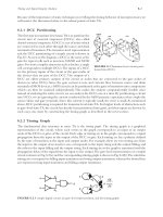
8.2.1 DCC Partitioning
The first step in transistor-level static TA is to partition the
circuit into dc connected components (DCCs), also called
channel-connected components. A DCC is a set of nodes which
are connected to each other through the source and drain
terminals of transistors. The transistor-level representation
and the DCC partitioning of a simple circuit is shown in
Fig. 8.1. As seen in the diagram, a DCC is the same as the
gate for typical cells such as inverters, NAND and NOR
gates. For more complex structures such as latches, a single
cell corresponds to multiple DCCs. The inputs of a DCC
are the primary inputs of the circuit or the gate nodes of
the devices that are part of the DCC. The outputs of a
DCC are either primary outputs of the circuit or nodes that are connected to the gate nodes of
devices in other DCCs. Since the gate current is zero and currents flow between source and drain
terminals of MOS devices, a MOS circuit can be partitioned at the gates of transistors into components
which can then be analyzed independently. This makes the analysis computationally feasible since
instead of analyzing the entire circuit, we can analyze the DCCs one at a time. By partitioning a circuit
into DCCs, we are ignoring the current conducted by the MOS parasitic capacitances that couple the
source/drain and gate terminals. Since this current is typically small, the error is small. As mentioned
above, DCC partitioning is required for transistor-level static TA. For higher levels of abstraction, such
as gate-level static TA, the circuit has already been partitioned into gates, and their inputs are known. In
such cases, one starts by constructing the timing graph as described in the next section.
8.2.2 Timing Graph
The fundamental data structure in static TA is the timing graph. The timing graph is a graphical
representation of the circuit, where each vertex in the graph corresponds to an input or an output
node of the DCCs or gates of the circuit. Each edge or timing arc in the graph corresponds to a signal
propagation from the input to the output of the DCC or gate. Each timing arc has a polarity defined
by the type of transition at the input and output nodes. For example, there are two timing arcs from
the input to the output of an inverter: one corresponds to the input rising and the output falling, and
the other to the input falling and the output rising. Each timing arc in the graph is annotated with the
propagation delay of the signal from the input to the output. The gate-level representation of a simple
circuit is shown in Fig. 8.2(a) and the corresponding timing graph is shown in Fig. 8.2(b). The solid-line
timing arcs correspond to falling input transitions and rising output transitions, whereas the dotted-line
arcs represent rising input transitions and falling output transitions.
FIGURE 8.1 Transistor-level circuit parti-
tioned into DCCs
FIGURE 8.2 A simple digital circuit: (a) gate-level representation, and (b) timing graph.
8-4 Memory, Microprocessor, and ASIC
Note that the timing graph may have cycles which correspond to feedback loops in the circuit.
Combinational feedback loops are broken and there are several strategies to handle sequential loops
(or cycles of latches).
5
In any event, the timing graph becomes acyclic and the vertices of the graph can
be arranged in topological order.
8.2.3 Arrival Times
Given the times at which the signals at the primary inputs or source nodes of the circuit are stable, the
minimum (earliest) and maximum (latest) arrival times of signals at all the nodes in the circuit can be
calculated with a single breadth-first pass through the circuit in topological order. The early arrival time
a(v) is the smallest time by which signals arrive at node v and is given by
(8.1)
Similarly, the late arrival time A(v) is the latest time by which signals arrive at node v and is given by
(8.2)
In the above equations, FI(v) is the set of all fan-in nodes of v, i.e., all nodes that have an edge to v and
d
uv
is the delay of an edge from u to v. Equations 8.1 and 8.2 will compute the arrival times at a node
v from the arrival times of its fan-in nodes and the delays of the timing arcs from the fan-in nodes to
v. Since the timing graph is acyclic (or has been made acyclic), the vertices in the graph can be arranged
in topological order (i.e., the DCCs and gates in the circuit can be levelized). A breadth-first pass
through the timing graph using Eqs. 8.1 and 8.2 will yield the arrival times at all nodes in the circuit.
Considering the example of Fig. 8.2, let us assume that the arrival times at the primary inputs a and
b are 0. From Eq. 8.2, the maximum arrival time for a rising signal at node a
1
is 1, and the maximum
arrival time for a falling signal is also 1. In other words, A
a1,r
= A
a1
,
f
=1, where the subscripts r and f
denote the polarity of the signal. Similarly, we can compute the maximum arrival times at node b
1
as
A
b1,r
=A
b1,f
=1, and at node d as A
d,r
=2 and A
d,f
=3.
In addition to the arrival times, we also need to compute the signal transition times (or slopes) at the
output nodes of the gates or DCCs. These transition times are required so that we can compute the
delay across the fan-out gates. Note that there are many timing arcs that are incident at the output
node and each gives rise to a different transition time. The transition time of the node is picked to be
the transition time corresponding to the arc that causes the latest (earliest) arrival time at the node.
8.2.4 Required Times and Slacks
Constraints are placed on the arrival times of signals at the primary output nodes of a circuit based on
performance or speed requirements. In addition to primary output nodes, timing constraints are
automatically placed on the clocked elements inside the circuit (e.g., latches, gated clocks, domino
logic gates, etc.). These timing constraints check that the circuit functions correctly and at-speed.
Nodes in the circuit where timing checks are imposed are called sink nodes.
Timing checks at the sink nodes inject required times on the earliest and latest signal arrival times
at these nodes. Given the required times at these nodes, the required times at all other nodes in the
circuit can be calculated by processing the circuit in reverse topological order considering each node
only once. The late required time R(v) at a node v is the required time on the late arriving signal. In
other words, it is the time by which signals are required to arrive at that node and is given by
(8.3)
8-5Timing and Signal Integrity Analysis
Similarly, the early required time r(v) is the required time on the early arriving signal. In other words, it
is the time after which signals are required to arrive at node v and is given by
(8.4)
In these equations, FO(v) is the set of fan-out nodes of v (i.e., the nodes to which there is a timing arc
from node v) and d
uv
is the delay of the timing arc from node u to node v. Note that R(v) is the time
before which a signal must arrive at a node, whereas r(v) is the time after which the signal must arrive.
The difference between the late arrival time and the late required time at a node v is defined as the
late slack at that node and is given by
(8.5)
Similarly, the early slack at node v is defined by
(8.6)
Note that the late and early slacks have been defined in such a way that a negative value denotes a
constraint violation. The overall slack at a node is the smaller of the early and late slacks; that is,
(8.7)
Slacks can be calculated in the backward traversal along with the required times. If the slacks at all
nodes in the circuit are positive, then the circuit does not violate any timing constraint. The nodes with
the smallest slack value are called critical nodes. The most critical path is the sequence of critical nodes that
connect the source and sink nodes.
Continuing with the example of Fig. 8.2, let the maximum required time at the output node d be
1. Then, the late required time for a rising signal at node a
1
is R
a1,r
=-0.5 since the delay of the rising-to-
falling timing arc from a
1
to d is 1.5. Similarly, the late required time for a falling signal at node a1 is
R
a1,f
=R
d,r
1=0. The required times at the other nodes in the circuit can be calculated to be: R
b1,r
=
-1,
R
b1,f
=0, R
a,r
=-1, R
a,f
=-1.5, R
b,r
=-1, and R
b,f
=-2. The slack at each node is the difference between the
required time and the arrival time and are as follows: S
d,r
=-1.5, S
d,f
=-2, S
al,r
=-1.5, S
a1,f
=-1, S
b1,r
= -2,
S
b1,f
=–1,S
a,r
=-1, S
a,f
=-1.5, S
b,r
=-1, and S
b,f
=-2. Thus, the critical path in this circuit is b falling—b1
rising—d falling, and the circuit slack is -2.
8.2.5 Clocked Circuits
As mentioned earlier, combinational circuits have timing checks imposed only at the circuit primary
outputs. However, for circuits containing clocked elements such as latches, flip-flops, gated clocks,
domino/precharge logic, etc., timing checks must also be enforced at various internal nodes in the
circuit to ensure that the circuit operates correctly and at-speed. In circuits containing clocked elements,
a separate recognition step is required to detect the clocked elements and to insert constraints. There
are two main techniques for detecting clocked elements: pattern recognition and clock propagation.
In pattern recognition-based approaches, commonly used sequential elements are recognized using
simple topological rules. For example. back-to-back inverters in the netlist are often an indication of a
latch. For more complex topologies, the detection is accomplished using templates supplied by the
user. Portions of a circuit are typically recognized in the graph of the original circuit by employing
subgraph isomorphism algorithms.
9
Once a subcircuit has been recognized, timing constraints are
automatically inserted. Another application of pattern-based subcircuit recognition is to determine
logical relationships between signals. For example, in pass-gate multiplexors, the data select lines are
typically one-hot. This relationship cannot be obtained from the transistor-level circuit representation
without recognizing the subcircuit and imposing the logical relationships for that subcircuit. The
logical relationship can then be used by timing analysis tools. However, purely pattern recognition-
8-6 Memory, Microprocessor, and ASIC
based approaches can be restrictive and may necessitate a large number of templates from the user for
proper functioning.
In clock propagation-based approaches, the recognition is performed automatically by propagating
clock signals along the timing graph and determining how these clock signals interact with data signals
at various nodes in the circuit. The primary input clocks are identified by the user and are marked as
(simple) clock nodes. Starting from the primary clock inputs and traversing the timing arcs in the
timing graph, the type of the nodes is determined based on simple rules. These rules are illustrated in
Fig. 8.3, where we show the transistor-level subcircuits and the corresponding timing subgraphs for
some common sequential elements.
FIGURE 8.3 Sequential element detection: (a) simple clock, (b) gated clock, (c) merged clock, (d) latch node, and
(e) footed and footless domino gates. Broken arcs are shown as dotted lines. Each arc is marked with the type of
output transition(s) it can cause (e.g., R/F: rise and fall, R: rise only, and F: fall only).
8-7Timing and Signal Integrity Analysis
• A node that has only one clock signal incident on it and no feedback is classified as a simple clock
node (Fig. 8.3(a)).
• A node that has one clock and one or more data signals incident on it, but no feedback, is
classified as a gated clock node (Fig. 8.3(b)).
• A node that has multiple clock signals (and zero or more data signals) incident on it and no
feedback is classified as a merged clock node (Fig. 8.3(c)).
• A node that has at least one clock and zero or more data signals incident on it and has a
feedback of length two (i.e., back-to-back timing arcs) is classified as a latch node (Fig. 8.3(d)).
The other node in the two-node feedback is called the latch output node. A latch node is of type
data. The timing arc(s) from the latch output node to the latch is (are) broken. Latches can be
of two types: level-sensitive and edge-triggered. To distinguish between edge-triggered and level-
sensitive latches, various rules may be applied. These rules are usually design-specific and will
not be discussed here. It is assumed that all latches are level-sensitive unless the user has marked
certain latches to be edge-triggered.
• Note that the domino gates of Fig. 8.3(e) also satisfy the conditions for a latch node. For a latch
node, both data and clock signals cause rising and falling transitions at the latch node. For
domino gates, data inputs a and b cause only falling transitions at the domino node x. This condition
can be used to distinguish domino nodes from latch nodes. Footed and footless domino gates
can be distinguished from each other by looking at the clock transitions on the domino node.
Since the footed gate has the clocked nMOS transistor at the “foot” of the evaluate tree, the
clock signal at CK causes both rising and falling transitions at node x. In the footless domino
gate, CK causes only a rising transition at node x.
Clock propagation stops when a node has been classified as a data node. This type of detection can be
easily performed with a simple breadth-first search on the timing graph.
Once the sequential elements have been recognized, timing constraints must be inserted to ensure that
the circuit functions correctly and at-speed.
10
These are described below and illustrated in Figs. 8.4 and 8.5.
• Simple clocks: In this case, no timing checks are necessary. The arrival times and slopes at the
simple clock node are obtained just as in normal data node.
• Gated clocks: The basic purpose of a gated clock is to enable or disable clock transitions at the
input of the gate from propagating to the output of the gate. This is done by setting the value
of the data input. For example, in the gated clock of Fig. 8.3(b), setting the data input to 1 will
allow the clock waveform to propagate to the output, whereas setting the data input to 0 will
disable transitions at the gate output. To make sure that this is indeed the behavior of the gated
clock, the timing constraints should be such that transitions at the data input node(s) do not
create transitions at the output node. For the gated NAND clock of Fig. 8.3(b), we have to
ensure that the data can transition (high or low) only when the clock is low, i.e., data can
transition after the clock turns low (short path constraint) and before the clock turns high (long
path constraint). This is shown in Fig. 8.4(a). In addition to imposing this timing constraint, we
also break the timing arc from the data node to the gated clock node since data transitions
cannot create output clock transitions.
• Merged clocks: Merged clocks are difficult to handle in static TA since the output clock waveform
may have a different clock period compared to the input clocks. Moreover, the output clock
waveform depends on the logical operation performed by the gate. To avoid these problems, static
TA tools typically ask the user to provide the waveform at the merged clock node and the merged
clock node is treated as a (simple) clock input node with that waveform. Users can obtain the clock
waveform at the merged clock node by using dynamic simulation with the input clock waveforms.
• Edge-triggered latches: An edge-triggered latch has two types of constraints: set-up constraint and
hold constraint. The set-up constraint requires that the data input node should be ready (i.e., the
rising and falling signals should have stabilized) before the latch turns on. In the latch shown in
Fig. 8.3(d), the latch is turned on by the rising edge of the clock. Hence, the data should arrive
8-8 Memory, Microprocessor, and ASIC
some time before the rising edge of the clock (this time margin is typically referred to as the set-
up time of the latch). This constraint imposes a required time on the latest (or maximum) arrival
time at the data input of the latch and is therefore a long path constraint. This is shown in Fig.
8.4(b). The hold constraint ensures that data meant for the current clock cycle does not
accidentally appear during the on-phase of the previous clock cycle. Looking at Fig. 8.4(b), this
implies that the data should appear some time after the falling edge of the clock (this time
margin is called the hold time of the latch). The hold time imposes a required time on the early
(or minimum) arrival time at the data input node and is therefore a short path constraint. As the
name implies, in edge-triggered latches, the on-edge of the clock causes data to be stored in the
latch (i.e., causes transitions at the latch node). Since the data input is ready before the clock
turns on, the latest arrival time at the latch node will be determined only by the clock signal. To
make sure that this is indeed the behavior of the latch, the timing arc from the data input node
to the latch node is broken, as shown in Fig. 8.4(b). One additional set of timing constraints is
imposed for an edge-triggered latch. Since data is stored at the latch (or latch output) node, we
must ensure that the data gets stored before the latch turns off. In other words, signals should
arrive at the latch output node before the off-edge of the clock.
• Level-sensitive latches: In the case of level-sensitive latches, the data need not be ready before the
latch turns on, as is the case for edge-triggered latches. In fact, the data can arrive after the on-
edge of the clock—this is called cycle stealing or time borrowing. The only constraint in this case is
that the data gets latched before the clock turns off. Hence, the set-up constraint for a level-
sensitive latch is that signals should arrive at the latch output node (not the latch node itself)
before the falling edge of the clock, as shown in Fig. 8.4(c). The hold constraint is the same as
FIGURE 8.4 Timing constraints and timing graph modifications for sequential elements: (a) gated clock, (b)
edge-triggered latch, and (c) level-sensitive latch. Broken arcs are shown as dotted lines.
8-9Timing and Signal Integrity Analysis
before; it ensures that data meant for the current clock cycle arrives only after the latch was
turned off in the previous clock cycle. This is also shown in Fig. 8.4(c). Since the latest arriving
signal at the latch node may come from either the data or the clock node, timing arcs are not
broken for a level-sensitive latch. Since data can flow through the latch, level-sensitive latches
are also referred to as transparent latches.
• Domino gates: Domino circuits have two distinct phases of operation: precharge and evaluate.
11
Looking at the domino gate of Fig. 8.3(e), we see that in the precharge phase, the clock signal
is low and the domino node x is precharged to a high value and the output node y is pre-
discharged to a low value. During the evaluate phase, the clock is high and if the values of the
gate inputs establish a path to ground, domino node x is discharged and output node y turns
high. The difference between footed and footless domino gates is the clocked nMOS transistor at
the “foot” of the nMOS evaluate tree. To demonstrate the timing constraints imposed on
domino circuits, consider the domino circuit block diagram and the clock waveforms shown in
Fig. 8.5. The footed domino blocks are labeled FD1 and FD2, and the footless blocks are
labeled FLD1 and FLD2. From Fig. 8.5(b), note that all three clocks have the same period 2T,
but the falling edge of CK2 is 0.25T after the falling edge of CK1 which in turn is 0.5T after the
falling edge of CK0. Therefore, the precharge phase for FD1 and FD2 is T, for FLD1 is 0.5T, and
for FLD2 is 0.25T. The various timing constraints for domino circuits are illustrated in Fig. 8.5
and discussed below.
1. We want the output O to evaluate (rise) before the clock starts falling and to precharge
(fall) before the clock starts rising.
FIGURE 8.5 Domino circuit: (a) block diagram, and (b) clock waveforms and precharge and evaluate constraints.
Note precharge implies the phase of operation (clock); the signals are falling.
8-10 Memory, Microprocessor, and ASIC
2. Consider node N1, which is an output of FD1 and an input of FD2. N1 starts precharging
(falling) when CK0 falls, and the constraint on it is that it should finish precharging before CK0
starts rising.
3. Next, consider node N2, which is an input to FLD1 clocked by CK1. Since this block is
footless, N2 should be low during the precharge phase to avoid short-circuit current. N2
starts precharging (falling) when CK0 starts falling and should finish falling before CK1 starts
falling. Note that the falling edges of CK0 and CK1 are 0.5T apart, and the precharge
constraint is on the late or maximum arrival time of N2 (long path constraint). Also, N2 should
start rising only after CK1 has finished rising. This is a constraint on the early or minimum
arrival time of N2 (short path constraint). In this example, N2 starts rising with the rising edge
of CK0 and, since all the clock waveforms rise at the same time, the short path constraint will
be satisfied trivially.
4. Finally, consider node N3. Since N3 is an input of FLD2, it must satisfy the short-circuit current
constraints. N3 starts precharging (falling) when CK1 starts falling and it should fall completely
before CK2 starts falling. Since the two clock edges are 0.25T apart, the precharge constraint on
N3 is tighter than the one on N2. As before, the short path constraint on N3 is satisfied trivially.
The above discussion highlights the various types of timing constraints that must be automatically
inserted by the static TA tool.
Note that each relative timing constraint between two signals is actually composed of two constraints.
For example, if signal d must rise before clock CK rises, then (1) there is a required time on the late or
maximum rising arrival time at node d (i.e., A
d,r
<A
CK,r
), and (2) there is a required time on the early or
minimum rising arrival time at the clock node CK (i.e., a
CK,r
<a
d,r
). There is one other point to be noted.
Set-up and hold constraints are fundamentally different in nature. If a hold constraint is violated, then
the circuit will not function at any frequency. In other words, hold constraints are functional constraints.
Set-up constraints, on the other hand, are performance constraints. If a set-up constraint is violated, the
circuit will not function at the specified frequency, but it will function at a lower frequency (lower
speed of operation). For domino circuits, precharge constraints are functional constraints, whereas
evaluate constraints are performance constraints.
8.2.6 Transistor-Level Delay Modeling
In transistor-level static TA, delays of timing arcs have to be computed on-the-fly using transistor-
level delay estimation techniques. There are many different transistor-level delay models which
provide different trade-offs between speed and accuracy. Before reviewing some of the more
popular delay models, we define some notations. We will refer to the delay of a timing arc as being
its propagation delay (i.e., the time difference between the output and the input completing half
their transitions). For a falling output, the fall times is defined as the time to transition from 90% to
10% of the swing; similarly, for a rising output, the rise time is defined as the time to transition
from 10% to 90% of the swing. The transition time at the output of the timing arc is defined to be
either the rise time or the fall time. In many of the delay models discussed below, the transition
time at the input of a timing arc is required to find the delay across the timing arc. At any node
in the circuit, there is a transition time corresponding to each timing arc that is incident on that
node. Since for long path static TA, we find the latest arriving signal at a node and propagate that
arrival time forward, the transition time at a node is defined to be the output transition time of
the timing arc which produced the latest arrival time at the node. Similarly, for short path analysis,
we find the transition time as the output transition time of the timing arc that produced the
earliest arrival time at the node.
Analytical closed-form formulae for the delay and output transition times are useful for static TA
because of their efficiency. One such model was proposed in Hedenstierna and Jeppson,
12
where the
propagation delay across an inverter is expressed as a function of the input transition time sin, the
8-11Timing and Signal Integrity Analysis
output load CL, and the size and threshold voltages of the NMOS and PMOS transistors. For example,
the inverter delay for a rising input and falling output is given by
(8–8)
where ß
n
is the NMOS transconductance (proportional to the width of the device), V
tn
is the NMOS
threshold voltage, and k
0
, k
1
, and k
2
are constants. The formula for the rising delay is the same, with
PMOS device parameters being used. The output transition time is considered to be a multiple of the
propagation delay and can be calibrated to a particular technology. More accurate analytical formulae
for the propagation delay and output transition time for an inverter gate have been reported in the
literature.
13,14
These methods consider more complex circuit behavior such as short-circuit current
(both NMOS and PMOS transistors in the inverter are conducting) and the effect of MOS parasitic
capacitances that directly couple the input and outputs of the inverter. More accurate models of the
drain current and parasitic capacitances of the transistor are also used. The main shortcoming of all
these delay models is that they are based on an inverter primitive; therefore, arbitrary CMOS gates seen
in the circuit must be mapped to an equivalent inverter.
15
This process often introduces large errors.
A simpler delay model is based on replacing transistors by linear resistances and using closed-form
expressions to compute propagation delays.
16,17
The first step in this type of delay modeling is to
determine the charging/discharging path from the power supply rail to the output node that contains
the switching transistor. Next, each transistor along this path is modeled as an effective resistance and
the MOS diffusion capacitances are modeled as lumped capacitances at the transistor source and drain
terminals. Finally, the Elmore time constant
18
of the path is obtained by starting at the power supply rail
and adding the product of each transistor resistance and the sum of all downstream capacitances
between the transistor and the output node. The accuracy of this method is largely dependent on the
accuracy of the effective resistance and capacitance models. The effective resistance of a MOS transistor
is a function of its width, the input transition time, and the output capacitance load. It is also a function
of the position of the transistor in the charging/discharging path. The position variable can have three
values: trigger (when the input at the gate of the transistor is switching), blocking (when the transistor is
not switching and it lies between the trigger and the output node), and support (when the transistor is
not switching and lies between the trigger and the power supply rail). The simplest way to incorporate
these effects into the resistance model is to create a table of the resistance values (using circuit
simulation) for various values of the transistor width, the input transition, and the output load. During
delay modeling, the resistance value of a transistor is obtained by interpolation from the calibration
table. Since the position is a discrete variable, a different table must be stored for each position variable.
The effective MOS parasitic capacitances are functions of the transistor width and can also be modeled
using a table look-up approach. The main drawbacks of this approach are the lack of accuracy in
modeling a transistor as a linear resistance and capacitance, as well as not considering the effect of
parallel charging/discharging paths and complementary paths. In our experience, this approach typically
gives 10–20% accuracy with respect to SPICE for standard gates (inverters, NANDs, NORs, etc.); for
complex gates, the error can be greater. These methods do not compute the transition time or slope at
the output of the DCC. The transition time at the output node is considered to be a multiple of the
propagation delay. Note that the propagation delay across a gate can be negative; this is the case, for
example, if there is a slow transition at the input of a strong but lightly loaded gate. As a result, the
transition time would become negative, giving a large error compared to the correct value.
Yet another method of modeling the delay from an input to an output of a DCC (or gate) is based
on running a circuit simulator such as SPICE,
5
or a fast timing simulator such as ILLIADS
6
or ACES.
7
Since the waveform at the switching input is known, the main challenge in this method is to determine
the assertions (whether an input should be set to a high or low value) for the side inputs which gives
rise to a transition at the output of the DCC.
19
For example, let us consider a rising transition at the
input causing a falling transition at the output. In this case, a valid assertion is one that satisfies the
8-12 Memory, Microprocessor, and ASIC
following two conditions: (1) before the transition, there should be no conducting path between the
output node and Gnd, and (2) after the transition, there should be at least one conducting path
between the output node and Gnd and no conducting path between the output node and V
dd
. The
sensitization condition for a rising output transition is exactly symmetrical. The valid assertions are
usually determined using a binary decision diagram.
20
For a particular input-output transition, there
may be many valid assertions; these valid assertions may have different delay values since the primary
charging/discharging path may be different or different node capacitances in the side paths may be
charged/discharged. To find the assertion that causes the worst-case (or best-case) delay, one may resort
to explicit simulations of all the valid assertions or employ other heuristics to prune out certain
assertions. The main advantage of this type of delay modeling is that very accurate delay and transition
time estimates can be obtained since the underlying simulator is accurate. The added accuracy is
obtained at the cost of additional runtime.
Since static timing analyzers typically use simple delay models for efficiency reasons, the top few
critical paths of the circuit should be verified using circuit simulation.
21,22
8.2.7 Interconnects and Static TA
As is well known, interconnects are playing a major role in determining the performance of current
microprocessors, and this trend is expected to continue in the next generation of processors.
23
The
effect of interconnects on circuit and system performance should be considered in an accurate and
efficient manner during static timing analysis. To illustrate interconnect modeling techniques, we will
use the example shown in Fig. 8.6(a) of a wire connecting a driving inverter to three receiving inverters.
The simplest interconnect model is to lump all the interconnect and receiver gate capacitances at
the output of the driver gate. This approximation may greatly overestimate the delay across the driver
gate since, in reality, all of the downstream capacitances are not “seen” by the driver gate because of
FIGURE 8.6 Handling interconnects in static TA: (a) a typical interconnect, (b) distributed RC model of
interconnect, (c) reduced -model to represent the loading of the interconnect, (d) effective capacitance loading,
and (e) propagation of waveform from root to sinks.
8-13Timing and Signal Integrity Analysis
resistive shielding due to line resistances. A more accurate model of the wire as a distributed RC line
is shown in Fig. 8.6(b). This is the wire model output by most commercial RC extraction tools. In Fig.
8.6(b), node r is called the root of the interconnect and is driven by the driver gate, and the other end
points of the wire at the inputs of the receiver gate are called sinks of the interconnect and are labeled
s
1
, s
2
,
and s
3.
Interconnects have two main effects: (1) the interconnect resistance and capacitance
determines the effective load seen by the driving gate and therefore its delay, and (2) due to non-zero
wire resistances, there is a non-zero delay from the root to the sinks of the interconnect—this is called
the time-of-flight delay.
To model the effect of the interconnect on the driver delay, we first replace the metal wire with a
-model load as shown in Fig. 8.6(c).
24
This is done by finding the first three moments of the admittance
Y(s) of the interconnect at node r. It can be shown that the admittance is given by
Next, we obtain the admittance of the -load as
where R, C
1
, and C
2
are the parameters of the -load model. To obtain the parameters of the -load,
we equate the first three moments of Y(s) and . This gives us the following equations for the
parameters of the -load model:
(8.9)
Now, if we are using a transistor-level delay model or a pre-characterized gate-level delay model that
can only handle purely capacitive loading and not -model loads, we have to determine an effective
capacitance C
eff
that will accurately model the -load. The basic idea of this method
25,26
is to equate the
average current drawn by the -model load to the average current drawn by the C
eff
load. Since the
average current drawn by any load is dependent on the transition time at the output of the gate and
the transition time is itself a function of the load, we have to iterate to converge to the correct value of
C
eff
. Once the effective capacitance has been obtained, the delay across the driver gate and the wave-
form at node r can be obtained.
The waveform at the root node is then propagated to the sink nodes s
1
, s
2
, s
3
across the transfer
functions H
1
(s), H
2
(s), and H
3
(s), respectively. This procedure is illustrated in Fig. 8.6(e). If the driver
waveform can be simplified as a ramp, the output waveforms at the sink nodes can be computed easily
using reduced-order modeling techniques like AWE
27
and the time-of-flight delay between the root
node and the sink nodes can be calculated.
8.2.8 Process Variations and Static TA
Unavoidable variations and disturbances present in IC manufacturing processes cause variations in
device parameters and circuit performances. Moreover, variations in the environmental conditions (of
such parameters as temperature, supply voltages, etc.) also cause variations in circuit performances.
28
As
a result, static TA should consider the effect of process and environmental variations. Typically, statistical
process and environmental variations are considered by performing analysis at two process corners: best-
case corner and worst-case corner. These process corners are typically represented as different device
model parameter sets, and as the name implies, are for the fastest and slowest devices. For gate-level
static TA, gate characterization is first performed at these two corners yielding two different gate delay
models. Then, static TA is performed with the best-case and worst-case gate delay models. Long path
constraints (e.g., latch set-up and performance or speech constraints) are checked with the worst-case
models and short path constraints (e.g., latch hold constraints) are checked with the best-case models.
8.2.9 Timing Abstraction
Transistor-level timing analysis is very important in high-performance microprocessor design and
verification since a large part of the design is hand-crafted and cannot be pre-characterized. Analysis at
8-14 Memory, Microprocessor, and ASIC
the transistor level is also important to accurately consider interconnect effects such as gate loading,
charge-sharing, and clock skew. However, full-chip transistor-level analysis of large microprocessor
designs is computationally infeasible, making timing abstraction a necessity.
Gate-Level Static TA
A straightforward extension of transistor-level static TA is to the gate level. At this level of abstraction,
the circuit has been partitioned into gates, and the inputs and outputs of each gate have been identi-
fied. Moreover, the timing arcs from the inputs to the outputs of a gate are typically pre-characterized.
The gates are characterized by applying a ramp voltage source at the input of the gate and an explicit
load capacitance at the output of the gate. Then, the transition time of the ramp and the value of the
load capacitance is varied, and circuit simulation (e.g., SPICE) is used to compute the propagation
delays and output transition times for the various settings. These data points can be stored in a table or
abstracted in the form of a curve-fitted equation. A popular curve-fitting approach is the k-factor
equations,
26
where the delay t
d
and output transition time t
out
are expressed as non-linear functions of
the input transition time s
in
and the capacitive output load C
L
:
(8
.
10)
(8.11)
The various coefficients in the k-factor equations are obtained by curve fitting the data. Several
modifications, including more complex equations and dividing the plane into a number of regions and
having equations for each region, have been proposed.
The main advantage of gate-level static TA is that costly on-the-fly delay and output transition time
calculations can be replaced by efficient equation evaluations or table look-ups. This is also a disadvantage
since it requires that all the timing arcs in the design are pre-characterized. This may be a problem when
parts of the design are not complete and the delays for some timing arcs are not available. This problem
can be avoided if the design flow ensures that at early stages of a design, estimated delays are specified for
all timing arcs which are then replaced by characterized numbers when the design gets completed. To
apply gate-level TA to designs that contain a large amount of custom circuits, timing rules must be
developed for the custom circuits also. Gate-level static TA is still at a fairly low level of abstraction and the
effects of interconnects and clock skew can be considered. Moreover, at the gate level, the latches and
flip-flops of the design are visible, so timing constraints can be inserted directly at those nodes.
Black-Box Modeling
At the next higher level of abstraction, gates are grouped together into blocks and the entire design (or
chip) now consists of these blocks or “boxes.” Each box contains combinational gates as well as sequential
elements such as latches as shown in Fig. 8.7(a). Timing checks inside the block can be verified using static
TA at the transistor or gate level. At the chip level, the internal nodes of the box are no longer visible and
its timing behavior must be abstracted at the input, output, and clock pins of the box. In black-box
modeling, we assume that the first and last latch along any path from input to output of the box are edge-
triggered latches; in other words, cycle stealing is not allowed across these latches (cycle stealing may be
allowed across other transparent latches inside the box). The first latch along a path from input to output
is called an input latch and the last latch is called an output latch. With this assumption, there can be two
types of paths to the outputs of the box. First, paths that originate at box inputs and end at box outputs
without traversing through any latches. These paths are represented as input-output arcs in the block-box
with the path delays annotated on the arcs. Second, there are paths that originate at the clock pins of the
output edge-triggered latches and end at the box outputs. These paths are represented as clock-to-input
arcs in the black-box and the paths delays are annotated on the arcs. Finally, the set-up and hold time
constraints of the input latches are translated to constraints between the box inputs and clock pins. These
constraints will be checked at the chip-level static TA. The constraints and the arcs are shown in Fig.
8-15Timing and Signal Integrity Analysis
8.7(b). Note that the timing checkpoints inside a block have been verified for a particular set of clocks
when the black-box model is generated. Since these timing checkpoints are no longer available at the
chip level, a black-box model is valid only for a particular frequency. If a different clock frequency (or
different clock waveforms) is used, then the black-box model must be regenerated.
Gray-Box Modeling
Gray-box modeling removes the edge-triggered latch restrictions of black-box modeling. All latches
inside the box are allowed to be level-sensitive and therefore have to be visible at the top level so that
the constraints can be checked and cycle-stealing is allowed through these latches. As shown in Fig.
8.7(c), the gray-box model consists of timing arcs from the box inputs to the input latches, from latches
to latches, and from the output latches to the box outputs. The clock pins of each of the latches are
also visible at the chip level, and so the set-up and hold time constraints for each latch in the box are
checked at the chip level. In addition to these timing arcs, there can also be direct input-output timing
arcs. Note that since the timing checkpoints internal to the box are available at the chip level, the gray-
box model is frequently independent—unlike the black-box model.
8.2.10 False Paths
To find the critical paths in the circuit, static TA propagates the arrival times from the timing inputs to
the timing outputs. Then, it propagates the required times from the outputs back to the inputs and
computes the slacks along the way. During propagation, static TA does not consider the logical func-
tionality of the circuit. As a result, some of the paths that it reports to the user may be such that they
cannot be activated by any input vector. Such paths are called false paths.
29–31
An example of a false
path is shown in Fig. 8.8(a). For x to propagate to a, we must set y=1, which is the non-controlling
value of the NAND gate. Similarly, for a to propagate to b, we set z=1. Now, since y=z=1, e=0 (the
controlling value for a NAND gate), and there can be no signal propagation from b to c. Therefore,
there can be no propagation from x to c (i.e., x–a–b–c is a false path). False paths that arise due to logical
correlations are called static false paths to distinguish them from dynamic false paths, which are caused by
temporal correlations.
FIGURE 8.7 High-level timing abstraction: (a) a block containing combinational and sequential elements, (b)
black-box model, and (c) gray-box model.
8-16 Memory, Microprocessor, and ASIC
A simple example of a dynamic false path is shown in Fig. 8.8(b). Suppose we want to find the critical
path from node x to the output d. It is clear that there are two such paths, x—a—d and x–a–b–c–d, of
which the latter has a larger delay. In order to sensitize the longer path x–a–b–c–d, we would set the
other inputs of the circuit to the non-controlling values of the gates (i.e., y=z=u=1). If there is a rising
transition on node x, there will be a falling transition on nodes a and c. However, because of the
propagation delay from a to c, node a will fall well before node c. As soon as node a falls, it will set the
primary output d to be 1 (since the controlling value of a NAND gate is 0). Because node a always
reaches the controlling value before node c, it is not possible for a transition at node c to reach the
output. In other words, the path x rising—a falling—b rising—c falling—d rising is a dynamic false path.
Note that if we add some combinational logic between the output of the first NAND gate and the
input of the last NAND gate to slow the signal a down, then the transition on c could propagate to the
output. The example shown above is for purposes of illustration only and may appear contrived.
However, dynamic false paths are very common in carry-lookahead adders.
32
Finding false paths in a combinational circuit is an NP-complete problem. There are a number of
heuristic approaches that find the longest paths in a circuit while determining and ignoring the false
paths.
29–31
Timing analysis techniques that can avoid false paths specified by the user have also been reported.
33,34
8.3 Noise Analysis
In digital circuits, nodes that are not switching are at the nominal values of the supply (logic 1) and
ground (logic 0) rails. In a digital system, noise is defined as a deviation of these node voltages from their
stable high or low values. Digital noise should be distinguished from physical noise sources that are
common in analog circuits (e.g., shot noise, thermal noise, flicker noise, and burst noise).
35
Since noise
causes a deviation in the stable logic voltages of a node, it can be classified into four categories: (1) high
undershoot noise reduces the voltage of a node that is supposed to be at logic 1; (2) high overshoot noise
which increases the voltage of a logic 1 node above the supply level (Vdd); (3) low overshoot noise
increases the voltage of a node that is supposed to be at logic 0; and (4) low undershoot noise which
reduces the voltage of a logic 0 node below the ground level (Gnd).
8.3.1 Sources of Digital Noise
The most common sources of noise in digital circuits are crosstalk noise, power supply noise, leakage
noise, and charge-sharing noise.
36
Crosstalk Noise
Crosstalk noise is the noise voltage induced on a net that is at a stable logic value due to interconnect
capacitive coupling with a switching net. The net or wire that is supposed to be at a stable value is
called the victim net. The switching nets that induce noise on the victim net are called aggressor nets.
Crosstalk noise is the most common source of noise in deep submicron digital designs because, as
interconnect wires get scaled, coupling capacitances become a larger fraction of the total wire
capacitances.
23
The ratio of the width to the thickness of metal wires reduces with scaling, resulting in
FIGURE 8.8 False path examples: (a) static false path, and (b) dynamic false path.
8-17Timing and Signal Integrity Analysis
a larger fraction of the total capacitance of the wire being contributed by coupling capacitances.
Several examples of functional failures caused by crosstalk noise are given in the section entitled,
“Crosstalk Noise Failures.”
Power Supply Noise
This refers to noise on the power supply and ground nets of a design that is passed onto the signal nets
by conducting transistors. Typically, the power supply noise has two components. The first is produced
by IR-drop on the power and ground nets due to the current demands of the various gates in the chip
(discussed in the next section). The second component of the power supply noise comes from the
RLC response of the chip and package to current demands that peak at the beginning of a clock
cycle. The first component of power supply noise can be reduced by making the wires that comprise
the power and ground network wider and denser. The second component of the noise can be
reduced by placing on chip decoupling capacitors.
37
Charge-Sharing Noise
Charge-sharing noise is the noise induced at a dynamic node due to charge redistribution between
that node and the internal nodes of the gate.
32
To illustrate charge-sharing noise, let us again consider
the two-input domino NAND gate of Fig. 8.9(a). Let us assume that during the first evaluate phase
shown in Fig. 8.9(b), both nodes x and x
1
are discharged. Then, during the next precharge phase, let us
assume that the input a is low. Node x will be precharged by the PMOS transistor MP, but x
1
will not
and will remain at its low value. Now, suppose CK turns high, signaling the beginning of another
evaluate phase. If during this evaluate phase, a is high but b is low, nodes x and x
1
will share charge,
resulting in the waveforms shown in Fig. 8.9(b): x will be pulled low and x
1
will be pulled high. If the
voltage on x is reduced by a large amount, the output inverter may switch and cause the output node
y to be wrongly set to a logic high value. Charge-sharing in a domino gate is avoided by precharging
the internal nodes in the NMOS evaluate tree during the precharge phase of the clock. This is done
by adding an anti charge sharing device such as MNc in Fig. 8.9(c) which is gated by the clock signal.
Leakage Noise
Leakage noise is due to two main sources: subthreshold conduction and substrate noise. Subthreshold leakage
current
32
is the current that flows in MOS transistors even when they are not conducting (off).This
current is a strong function of the threshold voltage of the device and the operating temperature.
Subthreshold leakage is an important design parameter in portable devices since battery life is directly
dependent on the average leakage current of the chip. Subthreshold conduction is also an important
noise mechanism in dynamic circuits where, for a part of the clock cycle, a node does not have a strong
conducting path to power or ground and the logic value is stored as a charge on that node. For
example, suppose that the inputs a and b in the two-input domino NAND gate of Fig. 8.9(a) are low
FIGURE 8.9 Example of charge-sharing noise: (a) a two-input domino NAND gate, (b) waveforms for charge-
sharing event, and (c) anti-charge-sharing device.
8-18 Memory, Microprocessor, and ASIC
during the evaluate phase of the clock. Due to subthreshold leakage current in the NMOS evaluate
transistors, the charge on node x may be drained away, leading to a degradation in its voltage and a
wrong value at the output node y. The purpose of the half latch device MPfb is to replenish the charge
that may be lost due to the leakage current.
Another source of leakage noise is minority carrier back injection into the substrate due to
bootstrapping. In the context of mixed analog-digital designs, this is often referred to as substrate noise.
38
Substrate noise is often reduced by having guard bands, which are diffusion regions around the active
region of a transistor tied to supply voltages so that the minority carriers can be collected.
8.3.2 Crosstalk Noise Failures
In this section, we provide some examples of functional failures caused by crosstalk noise. Functional
failures result when induced noise voltages cause an erroneous state to be stored at a memory element
(e.g., at a latch node or a dynamic node). Consider the simple latch circuit of Fig. 8.10 (a) and let us
assume that the data input d is a stable high value and the latch l has a stable low value. If the net
corresponding to node d is coupled to another net e and there is a high to low transition on net e, net
d will be pulled low. When e has finished switching, d will be pulled back to a high value by the PMOS
transistor driving net d and the noise on d will dissipate. Thus, the transition on net e will cause a noise
pulse on d. If the amplitude of this noise pulse is large enough, the latch node l will be pulled high.
Depending on the conditions under which the noise is injected, it may or may not cause a wrong
value to be stored at the latch node. For example, let us consider the situation depicted in Fig. 8.10 (b),
FIGURE 8.10 Crosstalk noise-induced functional failures: (a) latch circuit; (b) high undershoot noise on d does not
cause functional failure in (b) but does cause failure in (c); (d) same latch circuit with noise induced on an internal
node; and (e) low undershoot noise causing a failure.
8-19Timing and Signal Integrity Analysis
where CK is high and the latch is open. If the noise pulse on d appears near the middle of the clock
phase, then the latch node will be pulled high; but as the noise on d dissipates, latch node l will return
to its correct value because the latch is open. However, if the noise pulse on d appears near the end of
the clock phase as shown in Fig. 8.10 (c), the latch may turn off before the noise on d dissipates, the
latch node may not recover, and a wrong value will be stored. A similar unrecoverable error may occur
if noise appears on the clock net turning the latch on when it was meant to be off. This might cause
a wrong value to be latched.
Now let us consider the latch circuit of Fig. 8.10(d), where the wire between the input inverter and
the pass gate of the latch is long and subject to coupling capacitances. Suppose the latch is turned off
(CK is low), the data input is high so that the node d is low, and a high value is stored at the latch node.
If net e transitions from a high to a low value, a low undershoot noise will be introduced on d . If this
noise is sufficiently large, the NMOS pass transistor will turn on even through its gate voltage is zero
(since its gate-source voltage will become greater than its threshold voltage). This will discharge the
latch node l, resulting in a functional failure.
In order to push performance, domino circuits are becoming more and more prevalent.
88
These
circuits trade performance for noise immunity and are susceptible to functional noise failures. A noise-
related functional failure in domino circuits is shown in Fig. 8.11. Again, let us consider the two-input
domino NAND gate shown in Fig. 8.11(a). Let us assume that during the evaluate phase, a is held to a
low value by the driving inverter, but b is high. Then, x should remain charged and y should remain low.
If an unrelated net d switches high, and there is sufficient coupling between signals a and d, then a low
overshoot noise pulse will be induced on node a. If the pulse is large enough, a path to ground will be
created and node x will be discharged. As shown in Fig. 8.11(b), this will erroneously set the output
node of the domino gate to a high value. When the noise on a dissipates, it will return to a low value,
but x and y are not able to recover from the noise event, causing a functional failure.
As the examples above demonstrate, functional failures due to digital noise cause circuits to malfunction.
Noise analysis is becoming an important failure mechanism in deep submicron designs because of
several technology and design trends. First, larger die sizes and greater functionality in modern chips
result in longer wires, which makes the circuit more susceptible to coupling noise. Second, scaling of
interconnect geometries has resulted in increased coupling between adjacent wire.
23
Third, the drive
for faster performance has increased the use of faster non-restoring logic families such as domino logic.
These circuit families have faster switching speeds at the expense of reduced noise immunity. False
switching events at the inputs of these gates are catastrophic since precharged nodes may be discharged
and these nodes cannot recover their original state when the noise dissipates. Fourth, lower supply
voltage levels reduce the magnitudes of the noise margins of circuits. Finally, in state-of-the-art
microprocessors, many functional units located in different parts of the chip are operating in parallel
and this causes a lot of switching activity in long wires that run across different parts of the chip. All of
these factors make noise analysis a very important task to verify the proper functioning of digital
designs.
FIGURE 8.11 Functional failure in domino gates: (a) two-input NAND gate, and (b) voltage waveforms when
input noise causes a functional failure.
8-20 Memory, Microprocessor, and ASIC
8.3.3 Modeling of Interconnect and Gates for Noise Analysis
Let us consider the example of Fig. 8.12(a) where three wires are running in parallel and are capacitively
coupled to each other. Suppose that we are interested in finding the noise that is induced on the
middle net by the adjacent nets switching. The middle net is called the victim net and the two neighboring
nets are called aggressors. Consider the situation when the victim net is held to a stable logic zero value
by the victim driver and both the aggressor nets are switching high. Due to the coupling between the
nets, a low overshoot noise will be induced on the victim net as shown in Fig. 8.12(a). If the noise pulse
is large and wide enough, the victim receiver may switch and cause a wrong value at the output of the
inverter.
The circuit-level models for this system are explained below and shown in Fig. 8.12(b).
1. The (net) complex consisting of the victim and aggressor nets is modeled as a coupled distributed
RC network. The coupled RC lines are typically output by a parasitic extraction tool.
2. The non-linear victim driver is holding the victim net to a stable value. We model the non-linear
driver as a linear holding resistance. For example, if the victim driver holds the output to logic
0 (logic 1), we determine an effective NMOS (PMOS) resistance. The value of the holding
resistance for a gate can be obtained by pre-characterization using SPICE.
3. The aggressor driver is modeled as a Thevenin voltage source in series with a switching resistance.
The Thevenin voltage source is modeled as a shifted ramp, where the ramp starts switching at
time t
0
and the transition time is t. The switching resistance is denoted by R
s
.
4. The victim receiver is modeled as a capacitor of value equal to the input capacitance of the gate
These models convert the non-linear circuit into a linear circuit. The multiple sources in this
linear circuit can now be analyzed using linear superposition. For each aggressor, we get a noise
pulse at the sink(s) of the victim net, while shorting the other aggressors. These noise pulses have
different amplitudes and widths; the amplitude and width of the composite noise waveform is
obtained by aligning these noise pulses so that their peaks line up. This is a conservative assumption
to simulate the worst-case noise situation
FIGURE 8.12 (a) A noise pulse induced on the victim net by capacitive coupling to adjacent aggressor nets, and
(b) linearized model for analysis.
8-21Timing and Signal Integrity Analysis
8.3.4 Input and Output Noise Models
As mentioned earlier, noise creates circuit failures when it
propagates to a charge-storage node and causes a wrong
value to be stored at the node. Propagating noise across
non-linear gates
39
makes the noise analysis problem complex.
In this discussion, a more conservative simple model will be
discussed. With each input terminal of a victim receiver gate,
we associate a noise rejection curve.
40
This is a curve of the
noise amplitude versus the noise width that produces a
predefined amount of noise at the output. If we assume a
triangular noise pulse at the input of the victim receiver, the
noise rejection curve defines the amplitude-width combination that produces a fixed amount of
noise at the output of the receiver. A sample noise rejection curve is shown in Fig. 8.13. As the
width becomes very large, the noise amplitude tends toward the dc noise margin of the gate. Due
to the lowpass nature of a digital gate, very sharp noise pulses are filtered out and do not cause any
appreciable noise at the output. When the noise pulse at the sink(s) of the victim net have been
obtained, the pulse amplitude and width are compared against the noise rejection curve to
determine if a noise failure occurs.
Since we do not propagate noise across gates, noise injected into the victim net at the output of the
victim driver must model the maximum amount of noise that may be produced at the output of a gate.
The output noise model is a dc noise that is equal to the predefined amount of output noise that was
used to determine the input noise rejection curve above. Contributions from other dc noise sources
such as IR-drop noise may be added to the output noise. If we assume that there is no resistive dc path
to ground, this output noise appears unchanged at the sink(s) of the victim net.
8.3.5 Linear Circuit Analysis
The linear circuit that models the net complex to be analyzed can be quite large since the victim and
aggressor nets are modeled as a large number of RC segments and the victim net can be coupled to
many aggressor nets. Moreover, there are a large number of nets to be analyzed. Since general circuit
simulation tools such as SPICE can be extremely time-consuming for these networks, fast linear circuit
simulation tools such as RICE
41
can be used to solve these large net complexes. RICE uses reduced-
order modeling and asymptotic waveform evaluation (AWE) techniques
27
to speed up the analysis
while maintaining sufficient accuracy. Techniques that overcome the stability problems in AWE, such as
Pade via Lancszos (PVL),
42
Arnoldi-based techniques,
43
congruence transform-based techniques
(PACT),
44
or combinations (PRIMA),
45
have been proposed recently.
8.3.6 Interaction with Timing Analysis
Calculation of crosstalk noise interacts tightly with timing analysis since timing analysis lets us deter-
mine which of the aggressor nets can switch at the same time. This reduces the pessimism of
assuming that for a victim net, all the nets it is coupled to can switch simultaneously and induce
noise on it. Timing analysis defines timing windows by the earliest and latest arrival times for all
signals. This is shown in Fig. 8.14 for three aggressors A1, A2, and A3 of a particular victim net of
interest. Based upon these timing windows, we can define five different scenarios for noise analysis
where different aggressors can switch simultaneously. For example, in interval T1, only A1 can switch;
in T2, Al, and A2 can switch; in T3, only A2 can switch; and so on. Note that in this case, all three
aggressors can never switch at the same time. Without considering the timing windows provided by
timing analysis, we would have overestimated the noise by assuming that all three aggressors could
switch at the same time.
FIGURE 8.13 A typical noise rejection
curve.
8-22 Memory, Microprocessor, and ASIC
8.3.7 Fast Noise Calculation Techniques
Any state-of-the-art microprocessors will have many nets to be analyzed, but typically only a small
fraction of the nets will be susceptible to noise problems. This motivates the use of extremely fast
techniques that provably overestimate the noise at the sinks of a net. If a net passes the noise test under
this quick analysis, then it does not need to be analyzed any further; if a net fails the noise test, then it
can be analyzed using more accurate techniques. In this sense, these fast techniques can be considered
to be noise filters. If these noise filters produce sufficiently accurate noise estimates, then the expectation
is that a large number of nets would be screened out quickly. This combination of fast and detailed
analysis techniques would therefore speed up the overall analysis process significantly. Note that noise
filters must be provably pessimistic and that multiple noise filters with less and less pessimism can be
used one after the other to successively screen out nets.
Let us consider the net complex shown in Fig. 8.15(a), where we have modeled the net as distributed
RC lines, the victim driver as a linear holding resistance, and the aggressors as voltage ramps and linear
resistances. The grounded capacitances of the victim net is denoted as Cgv, and the coupling capacitances
to the two aggressors are denoted as C
c1
and C
c2
. In Figs. 8.15(b-d), we show the steps through which
we can obtain a circuit which will provide a provably pessimistic estimate of the noise waveform. In
Fig. 8.15(b), we have removed the resistances of the aggressor nets. This is pessimistic because, in reality,
FIGURE 8.14 Effect of timing windows on aggressor selection for noise analysis.
FIGURE 8.15 Noise filters: (a) original net complex with distributed RC models for aggressors and victims, (b)
aggressor lines have only coupling capacitances to victim, (c) aggressors are directly coupled to sink of victim, and
(d) single (strongest) aggressor and all grounded capacitors of victim moved away from sink.
8-23Timing and Signal Integrity Analysis
the aggressor waveform slows down as it proceeds along the net. By replacing it with a faster waveform,
more noise will be induced on the victim net. In Fig. 8.15(c), the aggressor waveforms are capacitively
coupled directly into the sink net; for each aggressor, the coupling capacitance is equal to the sum of
all the coupling capacitances between itself and the victim net. Since the aggressor is directly coupled
to the sink net, this transformation will result in more induced noise. In Fig. 8.15(d), we have made two
modifications; first, we replaced the different aggressors by one capacitively coupled aggressor and,
second, we moved all the grounded capacitors on the victim net away from the sink node. The
composite aggressor is just the fastest aggressor (i.e., the aggressor that has the smallest transition time)
and it is coupled to the victim net by a capacitor whose value is equal to the sum of all the coupling
capacitances in the victim net. To simplify the victim net, we sum all the grounded capacitors and insert
it at the root of the victim net and sum all the net resistances. By moving the grounded (good)
capacitors away from the sink net, we increase the amount of coupled noise. This simple network can
now be analyzed very quickly to compute the (pessimistic) noise pulse at the sink.
An efficient method to compute the peak noise amplitude at the sink of the victim net is described
by Devgan.
46
Under infinite ramp aggressor inputs, the maximum noise amplitude is the final value of
the coupled noise. For typical interconnect topologies, these analytical computations are simple and
quick.
8.3.8 Noise, Circuit Delays, and Timing Analysis
Circuit noise, especially crosstalk noise, significantly affects switching delays. Let us consider the ex-
ample of Fig. 8.16(a), where we are concerned about the propagation delay from A to C. In the
absence of any coupling capacitances, the rising waveform at C is shown by the dotted line of Fig.
8.16(b). However, if net 2 is switching in the opposite direction (node E is rising as in Fig. 8.16(b)), then
additional charge is pumped into net 1 due to the coupling capacitors causing the signals at nodes B
1
and B
2
to slow down. This in turn causes the inverter to switch later and causes the propagation delay
from A to C to be much larger, as shown in the diagram. Note that if net 2 switched in the same
direction as net 1, then the delay from A to C would be reduced. This implies that delays across gates
and wires depend on the switching activity on adjacent coupled nets. Since coupling capacitances are
a large fraction of the total capacitance of wires, this dependence will be significant and timing analysis
should account for this behavior. Using the same terminology as crosstalk noise analysis, we call the net
whose delay is of primary interest (net 1 in the above example) the victim net and all the nets that are
coupled to it are called aggressor nets.
A model that is commonly used to approximate the effect of coupling capacitors on circuit delays is
to replace each coupling capacitor by a grounded capacitor of twice the value. This model is accurate
only when the victim and aggressor nets are identical and the waveforms on the two nets are identical,
but switching in opposite directions. For some cases, doubling the coupling capacitance may be pessimistic,
but in many cases it is not—the effective capacitance is much more than twice the coupling capacitance.
FIGURE 8.16 Effect of noise on circuit delays: (a) victim and aggressor nets, and (b) typical waveforms.
8-24 Memory, Microprocessor, and ASIC
Note that the effect on the propagation delay due to coupling will be strongly dependent on how the
aggressor waveforms are aligned with respect to each other and to the victim waveform. Hence, one of
the main issues in finding the effect of noise on delay is to determine the aggressor alignments that
cause the worst propagation delay.
A more accurate model for considering the effect of noise
on delay is described by Dartu and Pileggi.
47
In this approach,
the gates are replaced by linearized models (e.g., the Thevenin
model of the gate consists of a shifted ramp voltage source in
series with a resistance). Once the circuit has been linearized,
the principle of linear superposition is applied. The voltage
waveform at the sink of the victim net is first obtained by
assuming that all aggressors are “quiet.” Then the victim net is
assumed to be quiet and each aggressor is switched one at a
time and the resultant noise waveforms at the victim sink
node is recorded. These noise waveforms are offset with
respect to each other because of the difference in the delays
between the aggressors and the victim sink node. Next, the aggressor noise waveforms are shifted such
that the peaks get lined up and a composite noise waveform is obtained by adding the individual noise
waveforms. The remaining issue is to align the composite noise waveform with the noise-free victim
waveform to obtain the worst delay. This process is described in Fig. 8.17, where we show the original
noise-free waveform V
orig
and the (composite) noise waveform V
noise
at the victim sink node. Then, the
worst case is to align the noise such that its peak is at the time when V
orig
=0.5V
dd
-V
N
, where V
N
is the
peak noise.
47,48
The final waveform at C ismarked V
final
.
The impact of noise on delays and the impact of timing windows on noise analysis implies that one
has to iterate between timing and noise analysis. There is no guarantee that this process will converge;
in fact, one can come up with examples when the process diverges. This is one of the open issues in
noise analysis.
8.4 Power Grid Analysis
The power distribution network distributes power and ground voltages to all the gates and devices in
the design. As the devices and gates switch, the power and ground lines conduct current and due to
the resistance of the lines, there is an unavoidable voltage drop at the point of distribution. This voltage
drop is called IR-drop. As device densities and switching currents increase, larger currents flow in the
power distribution network causing larger IR-drops. Excessive voltage drops in the power grid reduce
switching speeds of devices (since it directly affects the current drive of devices) and noise margins
(since the effective rail-to-rail voltage is lower). Moreover, as explained in the previous section, IR-
drops inject dc noise into circuits which may lead to functional or performance failures. Higher
average current densities lead to undesirable wear-and-tear of metal wires due to electromigration.
49
Considering all these issues, a robust power distribution network is vital in meeting performance and
reliability goals in high-performance microprocessors. This will achieve good voltage regulation at all
the consumption points in the chip, notwithstanding the fluctuations in the power demand across the
chip. In this section, we give a brief overview of various issues involved in power grid analysis.
8.4.1 Problem Characteristics
The most important characteristic of the power grid analysis problem is that it is a global problem. In
other words, the voltage drop in a certain part of the chip is related to the currents being drawn from
that as well as other parts of the chip. For example, if the same power line is distributing power to
several functional units in a certain part of the chip, the voltage drop in one functional unit depends on
the currents being drawn by the other functional units. In fact, as more and more of the functional
FIGURE 8.17 Aligning the composite
noise waveform with the original
waveform to produce worst-case delay.
8-25Timing and Signal Integrity Analysis
units switch together, the IR-drop in all the functional units will increase because the current supply
demand on the power line is more.
Since IR-drop analysis is a global problem and since power distribution networks are typically very
large, a critical issue is the large size of the network. For a state-of-the-art microprocessor, the number
of nodes in the power grid is on the order of millions. An accurate IR-drop analysis would simulate the
non-linear devices in the chip, together with the non-ideal power grid, making the size of the network
even more unmanageable. In order to keep IR-drop analysis computationally feasible, the simulation is
done in two steps. First, the non-linear devices are simulated assuming perfect supply voltages, and the
power and ground currents drawn by the devices are recorded (these are called current signatures). Next,
these devices are modeled as independent time-varying current sources for simulating the power grid
and the voltage drops at the consumption points (where transistors are connected to power and
ground rails) are measured. Since voltage drops are typically less than 10% of the power supply voltage,
the error incurred by ignoring the interaction between the device currents and the actual supply
voltage is usually small. The linear power and ground network is still very large and hierarchy has to be
exploited to reduce the size of the analyzed network. Hierarchy will be discussed in more detail later.
Yet another characteristic of the IR-drop analysis problem is that it is dependent on the activity in
the chip, which in turn is dependent on the vectors that are supplied. An important problem in IR-
drop analysis is to determine what this input pattern should be. For IR-drop analysis, patterns that
produce maximum instantaneous currents are required. This topic has been addressed by a few papers,
50–52
but will not be discussed here. However, the fact that vectors are important means that transient
analysis of the power grid is required. Since each solution of the network is expensive and since many
simulations are necessary, dynamic IR-drop analysis is very expensive. The speed and memory issues
related to linear system solution techniques become important in the context of transient analysis. An
important issue in transient analysis is related to the capacitances (both parasitic and intentional decoupling)
in the power grid. Since capacitors prevent instantaneous changes in node voltages, IR-drop analysis
without considering capacitors will be more pessimistic. A pessimistic analysis can be done by ignoring
all power grid capacitances, but a more accurate analysis with capacitances may require additional
computation time for solving the network.
Yet another issue is raised by the vector dependence. As mentioned earlier, the non-linear simulation
to determine the currents drawn from the power grid is done separately (from the linear network)
using the supplied vectors. Since the number of transistors in the whole chip is huge, simultaneous
simulation of the whole chip may be infeasible because of limitations in non-linear transient simulation
tools (e.g., SPICE or fast timing simulators). This necessitates partitioning the chip into blocks (typically
corresponds to functional units, like floating point unit, integer unit, etc.) and performing the simulation
one block at a time. In order to preserve the correlation among the different blocks, the blocks must
be simulated with the same underlying set of chip-wide vectors. To determine the vectors for a block,
a logic simulation of the chip is done, and the signals at the inputs of the block are monitored and used
as inputs for the block simulation.
Since dynamic IR-drop analysis is typically expensive (especially since many vectors are required),
techniques to reduce the number of simulations are often used. A commonly used technique is to
compress the current signatures from the different clock cycles into a single cycle. The easiest way to
accomplish this is to find the maximum envelope of the multi-cycle current signature. To find the
maximum envelope over N cycles, the single-cycle current signature is computed using
(8.12)
where i
sc
(t) is the single-cycle, i
orig
(t) is the original current signature, and T is the clock period. Since this
method does not preserve the correlation among different current sources (sinks), it may be overly
pessimistic.
A final characteristic of IR-drop analysis is related to the way in which the analysis is typically done.
Typically, the analysis is done at the very last stages of the design when the layout of the power network
is available. However, IR-drop problems that could be revealed at this stage are very expensive or even
8-26 Memory, Microprocessor, and ASIC
impossible to fix. IR-drop analysis that is applicable to all stages of a microprocessor design has been
addressed by Dharchoudhury et al.
53
8.4.2 Power Grid Modeling
The power and ground grids can be extracted by a parasitic extractor to obtain an R-only or an RC
network. Extraction implies that the layout of the power grid is available. To insert the transistor current
sources at the proper nodes in the power grid, the extractor should preserve the names and locations
of transistors. Power grid capacitances come from metal wire capacitances (coupling and grounded),
device capacitances, and decoupling capacitors inserted in the power grid to reduce voltage fluctua-
tions. Several interesting issues are raised in the modeling of power grid capacitances. The power or
ground net is coupled to other signal nets and since these nets are switching, the effective grounded
capacitance is difficult to compute. The same is true for capacitances of MOS devices connected to
the power grid. Making the problem worse, the MOS capacitances are voltage dependent. These issues
have not been completely addressed as yet. Typically, one resorts to worst-case analysis by ignoring
coupling capacitances to signal nets and MOS device capacitances, but considering only the grounded
capacitances of the power grid and the decoupling capacitors.
There are three other issues related to power grid modeling. First, for electromigration purposes, via
arrays should be extracted as resistance arrays so that current crowding can be modeled. Electromigration
problems are primarily seen in the vias and if the via array is modeled as a single resistance, such
problems could be masked. Second, the inductance of the package pins also creates a voltage drop in
the power grid. This drop is created by the time-varying current in the pins (v=Ldi/dt). This effect is
typically handled by adding a fixed amount of drop on top of the on-chip IR-drop estimate. Third, a
word of caution about network reduction or crunching. Most commercial extraction tools have options
to reduce the size of an extracted network. This reduction is typically performed using reduced-order
modeling techniques with interconnect delay being the target. This reduction is intended for signal
nets and is done so that errors in the interconnect delay are kept below a certain threshold. For IR-
drop analysis, such crunching should not be done since we are not interested in the delay. Moreover,
during the reduction the nodes at which transistors hook up to the power grid could be removed.
8.4.3 Block Current Signatures
As mentioned above, accurate modeling of the current signatures of the devices that are connected to
the power grid is important. At a certain point in the design cycle of a microprocessor, different blocks
may be at different stages of completion. This implies that multiple current signature models should be
available so that all the blocks in the design can be modeled at various stages in the design.
53
The most accurate model is to provide transient current signatures for all the devices that are
connected to the supply or ground grid. This assumes that the transistor-level representation of the
entire block is available. The transient current signatures are obtained by transistor-level simulation
(typically with a fast transient simulator) with user-specified input vectors. As mentioned earlier, in
order to maintain correlation with other blocks, the input vectors for each block must be derived from
a common chip-wide input vector set. At the chip level, the vectors are usually hot loops (i.e., the
vectors try to turn on as many blocks as possible). The block-level inputs for the transistor-level
simulation are obtained by monitoring the signal values at the block inputs during a logic simulation of
the entire chip with the hot loop vectors.
At the other end of the spectrum, the least accurate current model for a block is an area-based dc
current signature. This is employed at early stages of analysis when the block design is not complete.
The average current consumption per unit area of the block can be computed from the average power
consumption specification for the chip and the normal supply voltage value. Since the peak current
can be larger than the average current, some multiple of the average per-unit-area current is multiplied
by the block area to compute the current consumption for the block.
8-27Timing and Signal Integrity Analysis
An intermediate current model can be derived from a full-chip gate-level power estimation tool.
Given a set of input vectors, this tool computes the average power consumed by each block over a
cycle. From the average power consumption, an average current can be computed for each cycle.
Again, to account for the difference between the peak and average currents, the average current can
be multiplied by a constant factor. Hence, one obtains a multi-cycle dc current signature for the block
in this model.
8.4.4 Matrix Solution Techniques
The large size of power grids places very stringent demands on the linear system solver, making it the
most important part of an IR-drop analysis tool. The power grids in typical state-of-the-art micropro-
cessors usually contain multiple layers of metal (processes with up to six layers of metal are currently
available) and the grid is usually designed as a mesh. Therefore, the network cannot usually be reduced
significantly using a tree-link type of transformation. In older-generation microprocessors, the power
network was often “routed” and therefore more amenable to tree-link type reductions. In networks of
this type, significant reduction in the size can typically be obtained.
54
In general, matrix solution techniques can be categorized into two major types: direct and iterative.
55
The size and structure of the conductance matrix of the power grid is important in determining the
type of linear solution technique that should be used. Typically, the power grid contains millions of
nodes, but the conductance matrix is very sparse (typically, less than five entries per row or column of
the matrix). Since it is a conductance matrix, the matrix will also be symmetric positive definite—for a
purely resistive grid, the conductance matrix may be ill-conditioned.
Iterative solution techniques apply well to sparse systems, but their convergence can be slowed
down by ill-conditioning. Convergence can usually be improved by applying pre-conditioners. Another
important advantage of iterative methods is that they do not suffer from size limitations as much as
direct techniques. Iterative techniques usually need to store the sparse matrix and a few iteration
vectors during the solution. The disadvantage of iterative techniques is in transient solution. If constant
time steps are used during transient simulation, the conductance matrix remains the same from one
time point to another and only the right-hand-side vector changes. Iterative techniques depend on the
right-hand side and so a fresh solution is required for each time point during transient simulation. The
solution from previous time points cannot be reused. The most widely used iterative solution technique
for IR-drop analysis is the conjugate gradient solution technique. Typically, a pre-conditioner such as
incomplete Cholesky pre-conditioning is also used in conjunction with the conjugate gradient scheme.
Direct techniques rely on first factoring the matrix and then using these factors with the right-
hand-side vector to find the solution. Since the matrix is symmetric positive definite, one can apply
specialized direct techniques such as Cholesky factorization. The main advantage of direct techniques
in the context of IR-drop analysis is in transient analysis. As explained earlier, transient simulation with
constant time steps will result in the linear solution of a fixed matrix. Direct techniques can factor this
matrix once and the factors can be reused with different right-hand-side vectors to give some efficiency.
The main disadvantage of direct techniques is memory usage to store the factors of the conductance
matrix. Although the conductance matrix is sparse, its factors are not and this means that the memory
usage will be O(n
2
), where n is the size of the matrix.
8.4.5 Exploiting Hierarchy
From the discussions above, it is clear that IR-drop analysis of large microprocessor designs can be
limited by size restrictions. The most effective way to reduce the size is to exploit the hierarchy in the
design. In this discussion, we will assume a two-level hierarchy consisting of the chip and its constituent
blocks. This hierarchy in the blocks also partitions the entire power distribution grid into two parts: the
global grid and the intra-block grid. The global grid distributes power from the chip pads to tap points
in the various blocks (these are called block ports) and the intra-block grid distributes power from
these tap points to the transistors in the block. This partitioning allows us to apply hierarchical analysis.