MEMORY, MICROPROCESSOR, and ASIC phần 3 doc
Bạn đang xem bản rút gọn của tài liệu. Xem và tải ngay bản đầy đủ của tài liệu tại đây (1.07 MB, 42 trang )
3-15SRAM
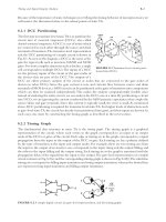
FIGURE 3.18 Noise-reduction output circuit. (From Izumikawa, M. et al., IEEE J. Solid-State Circuits, 32, 1, 52,
1997. With permission.)
FIGURE 3.19 Waveforms of noise-reduction output circuit (solid line) and conventional output circuit: (a) gate
bias, (b) data output, and (c) GND bounce. (From Miyaji, F. et al., IEEE Solid-State Circuits, 24, 5, 1213, 1989. With
permission.)
3-16 Memory, Microprocessor, and ASIC
inductance of the GND line. Therefore, the address buffer and the ATD circuit are influenced by the
GND bounce, and unnecessary signals are generated.
Figure 3.18 shows a noise-reduction output circuit. The waveforms of the noise-reduction output
circuit and conventional output circuit are shown in Fig. 3.19. In the conventional circuit, nodes A and
B are connected directly as shown in Fig. 3.18. Its operation and characteristics are shown by the
dotted lines in Fig. 3.18. Due to the high-speed driving of transistor M4, the GND potential goes up,
and the valid data is delayed by the output ringing. A new noise-reduction output circuit consists of
one PMOS transistor, two NMOS transistors, one NAND gate, and the delay part (its characteristics
are shown by the solid lines in Fig. 3.19). The operation of this circuit is explained as follows. The
control signals CE and OE are at high level and signal WE is at low level in the read operation. When
the data zero output of logical high level is transferred to node C, transistor M1 is cut off, and M2 raises
node A to the middle level. Therefore, the peak current that flows into the GND line through transistor
M4 is reduced to less than one half that of the conventional circuit because M4 is driven by the middle
level. After a 5-ns delay from the beginning of the middle level, transistor M3 raises node A to the VDD
level. As a result, the conductance of M4 becomes maximum, but the peak current is small because of
the low output voltage. Therefore, the increase of GND potential is small, and the output ringing does
not appear.
References
1. Bellaouar, A. and Elmasry, M.I., Low-Power Digital VLSI Design Circuit and Systems, Kluwer Academic
Publishers, 1995.
2. Ishibashi, K. et al., “A 1-V TFT-Load SRAM Using a Two-Step Word-Voltage Method,” IEEE J.
Solid-State Circuits, vol. 27, no. 11, pp. 1519–1524, Nov. 1992.
3. Chen, C W. et al., “A Fast 32KX8 CMOS Static RAM with Address Transition Detection,”
IEEE J. Solid-State Circuits, vol. SC-22, no. 4, pp. 533–537, Aug. 1987.
4. Miyaji, F. et al., “A 25-ns 4-Mbit CMOS SRAM with Dynamic Bit-Line Loads,” IEEE J. Solid-
State Circuits, vol. 24, no. 5, pp.1213–1217, Oct. 1989.
5. Matsumiya, M. et al., “A 15-ns 16-Mb CMOS SRAM with Interdigitated Bit-Line Architecture,”
IEEE J. Solid-State Circuits, vol. 27, no. 11, pp. 1497–1502, Nov. 1992.
6. Mizuno, H. and Nagano, T., “Driving Source-Line Cell Architecture for Sub-lV High-Speed
Low-Power Applications,” IEEE J. Solid-State Circuits, no. 4, pp. 552–557, Apr. 1996.
7. Morimura, H. and Shibata, N., “A Step-Down Boosted-Wordline Scheme for 1-V Battery-
Operated Fast SRAM’s,” IEEE J. Solid-State Circuits, no. 8, pp. 1220–1227, Aug. 1998.
8. Yoshimito, M. et al., “A Divided Word-Line Structure in the Static RAM and Its Application to
a 64 K Full CMOS RAM,” IEEE J. Solid-State Circuits, vol. SC-18, no. 5, pp. 479–485, Oct. 1983.
9. Hirose, T. et al., “A 20-ns 4-Mb CMOS SRAM with Hierarchical Word Decoding Architecture,”
IEEE J. Solid-State Circuits, vol. 25, no. 5, pp. 1068–1074, Oct. 1990.
10. Itoh, K., Sasaki, K., and Nakagome, Y., “Trends in Low-Power RAM Circuit Technologies,”
Proceedings of the IEEE, pp. 524–543, Apr. 1995.
11. Nambu, H. et al., “A 1.8-ns Access, 550-MHz, 4.5-Mb CMOS SRAM,” IEEE J. Solid-State
Circuits, vol. 33, no. 11, pp. 1650–1657, Nov. 1998.
12. Cararella, J.S., “A Low Voltage SRAM for Embedded Applications,” IEEE J. Solid-State Circuits,
vol. 32, no. 3, pp. 428–432, Mar. 1997.
13. Prince, B., Semiconductor Memories: A Handbook of Design, Manufacture, and Application, 2nd edition,
John Wiley & Sons, 1991.
14. Minato, O. et al., “A 20-ns 64 K CMOS RAM,” in ISSCC Dig. Tech. Papers, pp. 222–223, Feb.
1984.
15. Sasaki, K., et al., “A 9-ns 1-Mbit CMOS SRAM,” IEEE J. Solid-State Circuits, vol. 24, no. 5, pp.
1219–1224, Oct. 1989.
3-17SRAM
16. Seki, T. et al., “A 6-ns 1-Mb CMOS SRAM with Latched Sense Amplifier” IEEE J. Solid-State
Circuits, vol. 28, no. 4, pp. 478–482, Apr. 1993.
17. Kushiyama, N. et al., “An Experimental 295 MHz CMOS 4K X 256 SRAM Using Bidirectional
Read/Write Shared Sense Amps and Self-Timed Pulse Word-Line Drivers,” IEEE J. Solid-State
Circuits, vol. 30, no. 11, pp. 1286–1290, Nov. 1995.
18. Izumikawa, M. et al., “A 0.25-µm CMOS 0.9-V 100M-Hz DSP Core,” IEEE J. Solid-State
Circuits, vol. 32, no. 1, pp. 52–60, Jan. 1997.
4-1
4
Embedded Memory
4.1 Introduction 4-1
4.2 Merits and Challenges 4-2
On-Chip Memory Interface • System Integration • Memory
Size
4.3 Technology Integration and Applications 4-3
4.4 Design Methodology and Design Space 4-5
Design Methodology
4.5 Testing and Yield 4-6
4.6 Design Examples 4-7
A Flexible Embedded DRAM Design • Embedded Memories
in MPEG Environment • Embedded Memory Design for a 64-
bit Superscaler RISC Microprocessor
4.1 Introduction
As CMOS technology progresses rapidly toward the deep submicron regime, the integration level,
performance, and fabrication cost increase tremendously. Thus, low-integration, low-performance small
circuits or systems chips designed using deep submicron CMOS technology are not cost-effective.
Only high-performance system chips that integrate CPU (central processing unit), DSP (digital signal
processing) processors or multimedia processors, memories, logic circuits, analog circuits, etc. can afford
the deep submicron technology. Such system chips are called system-on-a-chip (SOC) or system-on-
silicon (SOS).
1,2
A typical example of SOC chips is shown in Fig. 4.1.
Embedded memory has become a key component of SOC and more practical than ever for at least
two reasons:
3
1. Deep submicron CMOS technology affords a reasonable trade-off for large memory integration
in other circuits. It can afford ULSI (ultra large-scale integration) chips with over 10
9
elements
on a single chip. This scale of integration is large enough to build an SOC system. This size of
circuitry inevitably contains different kinds of circuits and technologies. Data processing and
storage are the most primitive and basic components of digital circuits, so that the memory
implementation on logic chips has the highest priority. Currently in quarter-micron CMOS
technology, chips with up to 128 Mbits of DRAM and 500 Kgates of logic circuit, or 64 Mbits
of DRAM and 1 Mgates of logic circuit, are feasible.
2. Memory bandwidth is now one of the most serious bottlenecks to system performance. The
memory bandwidth is one of the performance determinants of current von Neuman-type
MPU (microprocessing unit) systems. The speed gap between MPUs and memory devices has
been increased in the past decade. As shown in Fig. 4.1, the MPU speed has improved by a
factor of 4 to 20 in the past decade. On the other hand, in spite of exponential progress in
storage capacity, minimum access times for each quadrupled storage capacity have improved
only by a factor of two, as shown in Fig. 4.2. This is partly due to the I/O speed limitation and
to the fact that major efforts in semiconductor memory development have focused on density
Chung-Yu Wu
National Chiao Tang University
0–8493–1737–1/03/$0.00+$ 1.50
© 2003 by CRC Press LLC
4-2 Memory, Microprocessor, and ASIC
and bit cost improvements. This speed gap creates a strong demand for memory integration
with MPU on the same chip. In fact, many MPUs with cycle times better than 60 ns have on-
chip memories. The new trend in MPUs, (i.e., RISC architecture) is another driving force for
embedded memory, especially for cache applications.
4
RISC architecture is strongly dependent
on memory bandwidth, so that high-performance, non-ECL-based RISC MPUs with more
than 25 to 50 MHz operation must be equipped with embedded cache on the chip.
4.2 Merits and Challenges
The main characteristics of embedded memories can be summarized as follows.
5
4.2.1 On-Chip Memory Interface
Advantages include:
1. Replacing off-chip drivers with smaller on-chip drivers can reduce power consumption
significantly, as large board wire capacitive loads are avoided. For instance, consider a system
which needs a 4-Gbyte/s bandwidth and a bus width of 256 bits. A memory system built with
discrete SDRAMs (16-bit interface at 100 MHz) would require about 10 times the power of
an embedded DRAM with an internal 256-bit interface.
2. Embedded memories can achieve much higher fill frequencies,
6
which is defined as the
bandwidth (in Mbit/s) divided by the memory size in Mbit (i.e., the fill frequency is the
number of times per second a given memory can be completely filled with new data), than
discrete memories. This is because the on-chip interface can be up to 512 bits wide, whereas
discrete memories are limited to 16 to 64 bits. Continuing the above example, it is possible to
make a 4-Mbit embedded DRAM with a 256-bit interface. In contrast, it would take 16
discrete 4-Mbit chips (256 K×16) to achieve the same width, so the granularity of such a
discrete system is 64 Mbits. But the application may only call for, say, 8 Mbits of memory.
3. As interface wire lengths can be optimized for application in embedded memories, lower propagation
times and thus higher speeds are possible. In addition, noise immunity is enhanced.
Challenges and disadvantages include:
FIGURE 4.1 An example of system-on-a-chip (SOC).
4-3Embedded Memory
1. Although the power consumption per system decreases, the power consumption per chip may
increase. Therefore, junction temperature may increase and memory retention time may decrease.
However, it should be noted that memories are usually low-power devices.
2. Some sort of minimal external interface is still needed in order to test the embedded memory.
The hybrid chip is neither a memory nor a logic chip. Should it be tested on a memory or
logic tester, or on both?
4.2.2 System Integration
Advantages include:
1. Higher system integration saves board space, packages, and pins, and yields better form factors.
2. Pad-limited design may be transformed into non-pad-limited by choosing an embedded solution.
3. Better speed scalability, along with CMOS technology scaling.
Challenges and disadvantages include:
1. More expensive packages may be needed. Also, memories and logic circuits require different
power supplies. Currently, the DRAM power supply (2.5 V) is less than the logic power supply
(3.3 V), but this situation will reverse in the future due to the back-biasing problem in DRAMs.
2. The embedded memory process adds another technology for which libraries must be developed
and characterized, macros must be ported, and design flows must be tuned.
3. Memory transistors are optimized for low leakage currents, yielding low transistor performance,
whereas logic transistors are optimized for high saturation currents, yielding high leakage currents.
If a compromise is not acceptable, expensive extra manufacturing steps must be added.
4. Memory processes have fewer layers of metal than do logic circuit processes. Layers can be
added at the expense of fabrication cost.
5. Memory fabs are optimized for large-volume production of identical products, for high-capacity
utilization, and for high yield. Logic fabs, while sharing these goals, are slanted toward lower
batch sizes and faster turnaround time.
4.2.3 Memory Size
The advantage is that:
• Memory size can be customized and memory architecture can be optimized for dedicated
applications.
Challenges and disadvantages include:
• On the other hand, the system designer must know the exact memory requirement at the time
of design. Later extensions are not possible, as there is no external memory interface. From the
customer’s point of view, the memory component goes from a commodity to a highly specialized
part that may command premium pricing. As memory fabrication processes are quite different,
second-sourcing problems abound.
4.3 Technology Integration and Applications
3,5
The memory technologies for embedded memories have a wide variation—from ROM to RAM—as
listed in Table 4.1.
3
In choosing these technologies, one of the most important figure of merits is the
compatibility to logic process.
1. Embedded ROM: ROM technology has the highest compatibility to logic process. However,
its application is rather limited. PLA, or ROM-based logic design, is a well-used but rather
special case of embedded ROM category. Other applications are limited to storage for
4-4 Memory, Microprocessor, and ASIC
microcode or well-debugged control code. A large size ROM for tables or dictionary
applications may be implemented in generic ROM chips with lower bit cost.
2. Embedded EPROM/E
2
PROM: EPROM/E
2
PROM technology includes high-voltage devices
and/or thin tunneling insulators, which require two to three additional mask steps and processing
steps to logic process. Due to its unique functionality, PROM-embedded MPUs
7
are well used. To
minimize process overhead, a single poly E
2
PROM cell has been developed.
8
Counterparts to this
approach are piggy-back packaged EPROM/MPUs or battery-backed SRAM/MPUs. However,
considering process technology innovation, on-chip PROM implementation is winning the game.
3. Embedded SRAM is one of the most frequently used memory embedded in logic chips.
Major applications are high-speed on-chip buffers such as TLB, cache, register file, etc. Table
4.2 gives a comparison of some approaches for SRAM integration. A six-transistor cell approach
may be the most highly compatible process, unless any special structures used in standard 6-Tr
SRAMs are employed. The bit density is not very high. Polysilicon resistor load 4-Tr cells
provide higher bit density with the cost of process complexity associated with additional
polysilicon-layer resistors. The process complexity and storage density may be compromised to
some extent using a single layer of polysilicon. In the case of a polysilicon resistor load SRAM,
which may have relaxed specifications with respect to data holding current, the requirement
for substrate structure to achieve good soft error immunity is more relaxed as compared to low
stand-by generic SRAMs. Therefore, the TFT (thin-film transistor) load cell may not be required
for several generations due to its complexity.
4. Embedded DRAM (eDRAM) is not as widely used as SRAMs. Its high density features, however,
are very attractive. Several different embedded DRAM approaches are listed in Table 4.3. A
trench or stacked cell used in commodity DRAMs has the highest density, but the complexity is
also high. The cost is seldom attractive when compared to a multi-chip approach using standard
DRAM, which is the ultimate in achieving low bit cost. This type of cell is well suited for ASM
(application-specific memory), which will be described in the next section. A planar cell with
TABLE 4.2 Embedded SRAM Options
TABLE 4.1 Embedded Memory Technologies and Applications
4-5Embedded Memory
multiple (double) polysilicon structures is also suitable for memory-rich applications.
9
A gate
capacitor storage cell approach can be fully compatible two with logic process providing relatively
high density.
10
The four-Tr cell (4-Tr SRAM cell minus resistive load) provides the same speed
and density as SRAM, but full compatibility to logic process and requires refresh operation.
11
4.4 Design Methodology and Design Space
3,5
4.4.1 Design Methodology
The design style of embedded memory should be selected according to applications. This choice is
critically important for the best performance and cost balancing. Figure 4.2 shows the various design
styles to implement embedded memories.
The most primitive semi-custom design style is based on the memory cell. It provides high flexibility
in memory architecture and short design TAT (turnaround time). However, the memory density is the
lowest among various approaches.
The structured array is a kind of gate array that has a dedicated memory array region in the master
chip that is configurable to several variations of memory organizations by metal layer customization.
Therefore, it provides relatively high density and short TAT. Configurability and fixed maximum memory
area are the limitations to this approach.
TABLE 4.3 Embedded DRAM Technology Options
FIGURE 4.2 Various design styles for embedded memories.
4-6 Memory, Microprocessor, and ASIC
The standard cell design has high flexibility to the extent that the cell library has a variety of
embedded memory designs. But in many cases, new system design requires new memory architectures.
The memory performance and density is high, but the mask-to-chip TAT tends to be long.
Super-integration is an approach that integrates existing chip design, including I/O pads, so the
design TAT is short and proven designs can be used. However, availability of memory architecture is
limited and the mask-to-chip TAT is long.
Hand-craft design (does not necessarily mean the literal use of human hands, but heavy interactive
design) provides the most flexibility, high performance, and high density; but design TAT is the longest.
Thus, design cost is the highest so that the applications are limited to high-volume and/or high-end
systems. Standard memories, well-defined ASMs, such as video memories,
12
integrated cache memories,
13
and high-performance MPU-embedded memories, are good examples.
An eDRAM (embedded DRAM) designer faces a design space that contains a number of dimensions
not found in standard ASICs, some of which we will subsequently review. The designer has to choose from
a wide variety of memory cell technologies which differ in the number of transistors and in performance.
Also, both DRAM technology and logic technology can serve as a starting point for embedding DRAM.
Choosing a DRAM technology as the base technology will result in high memory densities but suboptimal
logic performance. On the other hand, starting with logic technology will result in poor memory densities,
but fast logic circuits. To some extent, one can therefore trade logic speed against logic area. Finally, it is also
possible to develop a process that gives the best of both worlds—most likely at higher expense. Furthermore,
the designer can trade logic area for memory area in a way heretofore impossible.
Large memories can be organized in very different ways. Free parameters include the number of
memory banks, which allow the opening of different pages at the same time, the length of a single page,
the word width, and the interface organization. Since eDRAM allows one to integrate SRAMs and
DRAMs, the decision between on/off-chip DRAM- and SRAM/DRAM-partitioning must be made.
In particular, the following problems must be solved at the system level:
• Optimizing the memory allocation
• Optimizing the mapping of the data into memory such that the sustainable memory bandwidth
approaches the peak bandwidth
• Optimizing the access scheme to minimize the latency for the memory clients and thus minimize
the necessary FIFO depth
The goals are to some extent independent of whether or not the memory is embedded. However, the
number of free parameters available to the system designer is much larger in an embedded solution,
and the possibility of approaching the optimal solution is thus correspondingly greater. On the other
hand, the complexity is also increased. It is therefore incumbent upon eDRAM suppliers to make the
trade-offs transparent and to quantize the design space into a set of understandable if slightly subopti-
mal solutions.
4.5 Testing and Yield
3,5
Although embedded memory occupies a minor portion of the total chip area, the device density in the
embedded memory area is generally overwhelming. Failure distribution is naturally localized at memory
areas. In other words, embedded memory is a determinant of total chip yield to the extent that the
memory portion has higher device density weighted by its silicon area.
For a large memory-embedded VLSI, memory redundancy is helpful to enhance the chip yield.
Therefore, the embedded-memory testing, combined with the redundancy scheme, is an important
issue. The implementation of means for direct measurement of embedded memory on wafer as well as
in assembled samples is necessary.
4-7Embedded Memory
In addition to off-chip measurement, on-chip measurement circuitry is essential for accurate AC
evaluation and debugging. Testing DRAMs is very different from testing logic. In the following, the
main points of notice are discussed.
• The fault models of DRAMs explicitly tested for are much richer. They include bit-line and
word-line failures, crosstalk, retention time failures, etc.
• The test patterns and test equipment are highly specialized and complex. As DRAM test
programs include a lot of waiting, DRAM test times are quite high, and test costs are a significant
fraction of total cost.
• As DRAMs include redundancy, the order of testing is: (1) pre-fuse testing, (2) fuse blowing,
(3) post-fuse testing. There are thus two wafer-level tests.
The implication on eDRAMs is that a high degree of parallelism is required in order to reduce test costs.
This necessitates on-chip manipulation and compression of test data in order to reduce the off-chip
interface width. For instance, Siemens Corp. offers a synthesizable test controller supporting algorithmic
test pattern generation (ATPG) and expected-value comparison [partial built-in self test (BIST)].
Another important aspect of eDRAM testing is the target quality and reliability. If eDRAM is used
for graphics applications, occasional “soft” problems, such as too short retention time of a few cells, are
much more acceptable than if eDRAM is used for program data. The test concept should take this
costreduction potential into account, ideally in conjunction with the redundancy concept.
A final aspect is that a number of business models are common in eDRAM, from foundry business
to ASIC-type business. The test concept should thus support testing the memory, either from a logic
tester or a memory tester, so that the customer can do memory testing on his logic tester if required.
4.6 Design Examples
Three examples of embedded memory designs are described. The first one is a flexible embedded
DRAM design from Siemens Corp.
5
The second one is the embedded memories in MPEG environ-
ment from Toshiba Corp.
14
The last one is the embedded memory design for a 64-bit superscaler
RISC microprocessor from Toshiba Corp. and Silicon Graphics, Inc.
15
4.6.1 A Flexible Embedded DRAM Design
5
There is an increasing gap between processor and DRAM speed: processor performance increases by
60% per year in contrast to only a 10% improvement in the DRAM core. Deep cache structures are used
to alleviate this problem, albeit at the cost of increased latency, which limits the performance of many
applications. Merging a microprocessor with DRAM can reduce the latency by a factor of 5 to 10,
increase the bandwidth by a factor of 50 to 100, and improve the energy efficiency by a factor of 2 to 4.
16
Developing memory is a time-consuming task and cannot be compared with a high-level based
logic design methodology which allows fast design cycles. Thus, a flexible memory concept is a
prerequisite for a successful application of eDRAM. Its purpose is to allow fast construction of
application-specific memory blocks that are customized in terms of bandwidth, word width, memory
size, and the number of memory banks, while guaranteeing first-time-right designs accompanied by all
views, test programs, etc.
A powerful eDRAM approach that permits fast and safe development of embedded memory modules
is described. The concept, developed by Siemens Corp. for its customers, uses a 0.24-µm technology
based on its 64/256 Mbit SDRAM process.
5
Key features of the approach include:
• Two building-block sizes, 256 Kbit and 1 Mbit; memory modules with these granularities can
be constructed
• Large memory modules, from 8 to 16 Mbit upwards, achieving an area efficiency of about 1
Mbit/mm
2
4-8 Memory, Microprocessor, and ASIC
• Embedded memory sizes up to at least 128 Mbits
• Interface widths ranging from 16 to 512 bits per module
• Flexibility in the number of banks as well as the page length
• Different redundancy levels, in order to optimize the yield of the memory module to the
specific chip
• Cycle times better than 7 ns, corresponding to clock frequencies better than 143 MHz
• A maximum bandwidth per module of about 9 Gbyte/s
• A small, synthesizable BIST controller for the memory (see next section)
• Test programs, generated in a modular fashion
Siemens Corp. has made eDRAMs since 1989 and has a number of possible applications of its eDRAM
approach in the pipeline, including TV scan-rate converters, TV picture-in-picture chips, modems, speech-
processing chips, hard-disk drive controllers, graphics controllers, and networking switches. These applica-
tions cover the full range of memory sizes (from a few Mbits to 128 Mbits), interface widths (from 32 to 512
bits), and clock frequencies (from 50 to 150 MHz), which demonstrates the versatility of the concept.
4.6.2 Embedded Memories in MPEG Environment
14
Recently, multimedia LSIs, including MPEG decoders, have been drawing attention. The key require-
ments in realizing multimedia LSIs are their low-power and low-cost features. This example presents
embedded memory-related techniques to achieve these requirements, which can be considered as a
review of the state-of-the-art embedded memory macro techniques applicable to other logic LSIs.
Figure 4.3 shows embedded memory macros associated with the MPEG2 decoder. Most of the
functional blocks use their own dedicated memory blocks and, consequently, memory macros are
rather small and distributed on a chip. Memory blocks are also connected to a central address/data bus
for implementing direct test mode.
FIGURE 4.3 Block diagram of MPEG2 decoder LSI.
4-9Embedded Memory
An input buffer for the IDCT is shown in Fig. 4.4. Eight 16-bit data from D0 to D7 come from the
inverse quantization block sequentially. The stored data should then be read out as 4-bit chunks
orthogonal to the input sequence. The 4-bit data is used to address a ROM in the IDCT to realize a
distributed arithmetic algorithm.
The circuit diagram of an orthogonal memory whose circuit diagram is shown in Fig. 4.5. It realizes
the above-mentioned functionality with 50% of the area and the power that would be needed if the
IDCT input buffer were built with flip-flops. In the orthogonal memory, word-lines and bit-lines run
both vertically and horizontally to achieve the functionality. The macro size of the orthogonal memory
is 420 µm×760 µm, with a memory cell size of 10.8 µm×32.0 µm.
FIGURE 4.4 Input buffer structure for IDCT.
FIGURE 4.5 Circuit diagram of orthogonal memory.
4-10 Memory, Microprocessor, and ASIC
FIFOs and other dual-port memories are designed using a single-port RAM operated twice in one
clock cycle to reduce area, as shown in Fig. 4.6. A dual-port memory cell is twice as large as a single-
port memory cell.
All memory blocks are synchronous self-timed macros and contain address pipeline latches. Otherwise,
the timing design needs more time, since the lengths of the interconnections between latches and a
decoder vary from bit to bit. Memory power management is carried out using a Memory Macro
Enable signal when a memory macro is not accessed, which reduces the total memory power to 60%.
Flip-flop (F/F) is one of the memory elements in logic LSIs. Since digital video LSIs tend to
employ several thousand F/Fs on a chip, the design of the F/F is crucial for small area and low power.
The optimized F/F with hold capability is shown in Fig. 4.7. Due to the optimized smaller transistor
sizes, especially for clock input transistors, and a minimized layout accomodating a multiplexer and a
D-F/F in one cell, 40% smaller power and area are realized compared with a normal ASIC F/F.
Establishing full testability of on-chip memories without much overhead is another important issue.
Table 4.4 compares three on-chip memory test strategies: a built-in self-test (BIST), a scan test, and a
direct test. The direct test mode, where all memories can be directly accessed from outside in a test mode,
is implemented because of its inherent small area. In a test mode, DRAM interface pads are turned into
test pins and can access to each memory block through internal buses, as shown in Figs. 4.3 and 4.8.
FIGURE 4.6 Realizing dual-port memory with a single-port memory (FIFO case).
FIGURE 4.7 Optimized flip-flop.
4-11Embedded Memory
The present MPEG2 decoder contains a RISC whose firmware is stored in an on-chip ROM. In
order to make the debugging easy and extensive, an instruction RAM is put outside the pads in parallel
to the instruction ROM and activated by an Al-masterslice in an initial debugging stage as shown in
Fig. 4.9. For a sample chip mounted in a plastic package, the instruction RAM is cut out by a scribe
line. This scheme enables extensive debugging and early sampling at the same time for firmware-ROM
embedded LSIs.
4.6.3 Embedded Memory Design for a 64-bit Superscaler RISC Microprocessor
15
High-performance embedded memory is a key component in VLSI systems because of the high-speed
and wide bus width capability eliminating inter-chip communication. In addition, multi-ported buffer
memories are often demanded on a chip. Furthermore, a dedicated memory architecture that meets
the special constraint of the system can neatly reduce the system critical path.
On the other hand, there are several issues in embedded RAM implementation. The specialty or
variety of the memories could increase design cost and chip cost. Reading very wide data causes large
power dissipation. Test time of the chip could be increased because of the large memory. Therefore,
design efficiency, careful power bus design, and careful design for testability are necessary.
TABLE 4.4 Comparison of Various Memory Test
Strategies
FIGURE 4.8 Direct test architecture for embedded memories.
o: Good D: Fair X: Poor
4-12 Memory, Microprocessor, and ASIC
TFP is a high-speed and highly concurrent 64-bit superscaler RISC microprocessor, which can
issue up to four instructions per cycle.
17,18
Very wide bandwidth of on-chip caches is vital in this
architecture. The design of the embedded RAMs, especially on caches and TLB, is reported.
The TFP integer unit (IU) chip implements two integer ALU pipelines and two load/store pipelines.
The block diagram is shown in Fig. 4.10. A five-stage pipeline is shown in Fig. 4.11. In the TFP IU
chip, RAM blocks occupy a dominant part of the real estate. The die size is 17.3 mm×17.3 mm. In
addition to other caches, TLB, and register file, the chip also includes two buffer queues: SAQ (store
address queue) and FPQ (floating point queue). Seventy-one percent of all overall 2.6 million transistors
are used for memory cells. Transistor counts of each block are listed in Table 4.5.
The first generation of TFP chip was fabricated using Toshiba’s high-speed 0.8 µm CMOS technology:
double poly-Si, triple metal, and triple well. A deep n-well was used in PLL and cache cell arrays in
order to decouple these circuits from the noisy substrate or power line of the CMOS logic part. The
chip operates up to 75 MHz at 3.1 V and 70°C, and the peak performance reaches 300 MIPS.
Features of each embedded memory are summarized in Table 4.6. Instruction, branch, and data
caches are direct mapped because of the faster access time. High-resistive poly-Si load cells are used for
these caches since the packing density is crucial for the performance.
FIGURE 4.9 Instruction RAM masterslice for code debugging.
FIGURE 4.10 Block diagram of TFP IU.
4-13Embedded Memory
Instruction cache (ICACHE) is 16 KB of virtual address memory. It provides four instructions (128
bits wide) per cycle. Branch cache (BCACHE) contains branch target address with one flag bit to indicate
a predicted branch. BCACHE contains 1-K entries and is virtually indexed in parallel with ICACHE.
Data cache (DCACHE) is 16 KB, dual ported, and supports two independent memory instructions
(two loads, or one load and one store) per cycle. Total memory bandwidth of ICACHE and DCACHE
reaches 2.4 GB/s at 75 MHz. Floating point load/store data bypass DCACHE and go directly to
bigger external global cache.
17,19
DCACHE is virtually indexed and physically tagged.
TLB is dual ported, three-set-associative memory containing 384 entries. A unique address comparison
scheme is employed here, which will be described in the following section. It supports several different
page sizes, ranging from 4 KB to 16 MB. TLB is indexed by low-order 7 bits of virtual page number
(VPN). The index is hashed by exclusive-OR with a low-order ASID (address space identifier) so that
many processes can coexist in TLB at one time.
Since several different RAMs are used in TFP chips, the design efficiency is important. Consistent
circuit schemes are used for each of the caches and TLB RAMs. Layout is started from the block that
has the tightest area restriction, and the created layout modules are exported to other blocks with small
modification.
The basic block diagram of cache blocks is shown in Fig. 4.12, and the timing diagram is shown in Fig.
4.13. Unlike a register file or other smaller queue buffers, these blocks employ dual-railed bit-lines. To
achieve 75-MHz operation in the worst-case condition, it should operate at 110 MHz under typical
conditions. In this targeted 9-ns cycle time, address generation is done about 3 ns before the end of the
cycle, as shown in Fig. 4.11. To take advantage of this big address setup time, address is received by
transparent latch: TLAT_N (transparent while clock is low) instead of flip-flop. Thus, decode is started as
FIGURE 4.11 TFP IU pipelining.
TABLE 4.5 Transistor Counts
4-14 Memory, Microprocessor, and ASIC
TABLE 4.6 Summary of Embedded RAM Features
FIGURE 4.12 Basic RAM block diagram.
4-15Embedded Memory
soon as address generation is done and is finished before the end of the cycle. Another transparent
latch—TLAT_P (transparent while clock is high)—is placed after the sense amplifier and it holds read
data while the clock is low.
Word-line (WL) is enabled while clock is high. Since the decode is already finished, WL can be driven
to “high” as fast as possible. The sense amplifier is enabled (SAE) with a certain delay after the word-line.
The paired current-mirror sense amplifier is chosen since it provides good performance without overly
strict SAE timing. Bit-line is precharged and equalized while the clock is low. The clock-to-data delay of
DCACHE, which is the biggest array, is 3.7 ns under typical conditions: clock-to-WL is 0.9 ns and WL-
to-data is 2.8 ns. Since on-chip PLL provides 50% duty clock, timing pulses such as SAE or WE (write
enable) are created from system clock by delaying the positive edge and negative edge appropriately.
As both word-line and sense amplifier are enabled in just half the time of one cycle, the current
dissipation is reduced by half. However, the power dissipation and current spike are still an issue
because the read/write data width is extremely large. Robust power bus matrix is applied in the cache
and TLB blocks so that the dc voltage drop at the worst place is limited to 60 mV inside the block.
From a minimum cycle time viewpoint, write is more critical than read because write needs bigger
bit-line swing, and the bit-line must be precharged before the next read. To speed up precharge time,
precharge circuitry is placed on both the top and bottom of the bit-line. In addition, the write circuitry
dedicated to cache-refill is placed on the top side of DCACHE and ICACHE to minimize the wire
delay of the write data from input pad. Write data bypass selector is implemented so that the write data
is available as read data in the same cycle with no timing penalty.
Virtual to physical address translation and following cache hit check are almost always one of the
critical paths in a microprocessor. This is because the cache tag comparison has to wait for the VTLB
(RAM that contains virtual address tag) search operation and the following physical address selection
from PTLB (RAM that contains physical address).
20
A timing example of the conventional scheme is
shown in Fig. 4.14. In TFP, the DCACHE tag is directly compared with all the three sets of PTLB data
in parallel—which are merely candidates of physical address at this stage—without waiting for the
VTLB hit results. The block diagram and timing are shown in Figs. 4.15 and 4.16. By the time this hit
check of the cache tag is done, VTLB hit results are just ready and they select the PTLB hit result
immediately. The “ePmatch” signal in Fig. 4.16 is the overall cache hit result. Although three times
more comparators are needed, this scheme saves about 2.8 ns as compared to the conventional one.
FIGURE 4.13 RAM timing diagram.
4-16 Memory, Microprocessor, and ASIC
In TLB, sense amplifiers of each port are separately placed on the top and bottom of the array to
mitigate the tight layout pitch of the circuit. A large amount of wire creates problems around VTLB,
PTLB, and DTAG (DCACHE tag RAM) from both layout and critical path viewpoints. This was
solved by piling them to build a data path (APATH: Address Data Path) by making the most of the
metal-3 vertical interconnection. Although this metal-3 signal line runs over TLB arrays in parallel
with the metal-1 bit-line, the TLB access time is not degraded since horizontal metal-2 word-line
shields the bit-line from the coupling noise. The data fields of three sets are scrambled to make the data
path design tidy; 39-bit (in VTLB) and 28-bit (in PTLB) comparators of each set consist of optimized
AND-tree. Wired-OR type comparators are rejected because a longer wired-OR node in this array
configuration would have a speed penalty.
FIGURE 4.14 Conventional physical cache hit check.
FIGURE 4.15 TFP physical cache hit check.
4-17Embedded Memory
As TFP supports different page sizes, VPN and PFN (page frame number) fields change, depending
on the page size. The index and comparison field of TLB are thus made selectable by control signals.
32-bit DCACHE data are qualified by one valid bit. A valid bit needs the read-modify-write
operation based on the cache hit results. However, this is not realized in one cycle access because of
tight timing. Therefore, two write ports are added to valid bit and write access is moved to the next
cycle: the W-stage. The write data bypass selector is essential here to avoid data hazards.
To minimize the hardware overhead of the VRAM (valid bit RAM) row decoder, two schemes are
applied. First, row decoders of read ports are shared with DCACHE by pitch-matching one VRAM
cell height with two DCACHE cells. Second, write word-line drivers are made of shift registers that
have read word-lines as inputs. The schematic is shown in Fig. 4.17.
Although the best way to verify the whole chip layout is to do DRC (design rule check) and LVS
(layout versus schematic) check that includes all sections and the chip, it was not possible in TFP since
the transistor count is too large for CAD tools to handle. Thus, it was necessary to exclude a large part
of the memory cells from the verification flow. To avoid possible mistakes around the boundary of the
memory cell array, a few rows and columns were sometimes retained on each of the four sides of a cell
array. In the case when this breaks signal continuity, text is added on the top level of the layout to make
FIGURE 4.16 Block diagram of TLB and DTAG.
FIGURE 4.17 VRAM row decoder.
4-18 Memory, Microprocessor, and ASIC
a virtual connection, as shown in Fig. 4.18. These works are basically handled by CAD software plus
small programming without editing the layout by hand.
Direct testing of large on-chip memory is highly preferable in VLSI because of faster test time and
complete test coverage. TFP IU defines cache direct test in JTAG test mode, in which cache address,
data, write enable, and select signals are directly controlled from the outside. Thus, very straightforward
evaluation is possible. Utilizing a 64-bit, general-purpose bus that runs across the chip, the additional
hardware for the data transfer is minimized.
Since defect density is a function of device density and device area, large on-chip memory can be
a determinant of total chip yield. Raising embedded memory yield can directly lead to the rise of the
chip yield. Failure symptoms of the caches have been analyzed by making a fail-bit-map, and this has
been fed back to the fabrication process.
References
1. Borel, J., Technologies for Multimedia Systems on a Chip. In 1997 International Solid State Circuits
Conference, Digest of Technical Papers, 40, 18–21, Feb. 1997.
2. De Man, H., Education for the Deep Submicron Age: Business as Usual?, in Proceedings of the 34th
Design Automation Conference, p. 307–312, June 1997.
3. Iizuka, T., Embedded Memory: A Key to High Performance System VLSIs. Proceedings of 1990
Symposium on VLSI Circuits, p. 1–4, June 1990.
4. Horowitz, M., Hennessy, J., Chow, P., Gulak, P., Acken, J., Agrawal, A., Chu, C., McFarling, S.,
Przybylski, S., Richardson, S., Salz, A., Simoni, R., Stark, D., Steenkiste, P., Tjiang, S., and Wing,
M., A 32b Microprocessor with On-Chip 2K-Byte Instruction Cache. ISSCC Dig. of Tech. Papers,
p. 30–31, Feb. 1987.
5. Wehn, N. and Hein, S., Embedded DRAM Architectural Trade-offs. Proceedings of Design, Automation
and Test in Europe, p. 704–708, 1998.
FIGURE 4.18 RAM layout verification.
4-19Embedded Memory
6. Przybylski, S.A., New DRAM Technologies: A Comprehensive Analysis of the New Architectures.
Report, 1996.
7. Wada, Y., Maruyama, T., Chida, M., Takeda, S., Shinada, K., Sekiguchi, K., Suzuki, Y., Kanzaki, K.,
Wada, M., and Yoshikawa, M., A 1.7-Volt Operating CMOS 64 KBit E2PROM. Symp. on VLSI
Circ., Kyoto, Dig. of Tech. Papers, p. 41–42, May 1989.
8. Matsukawa, M., Morita, S., Shinada, K., Miyamoto, J., Tsujimoto, J., Iizuka, T., and Nozawa, H., A
High Density Single Poly Si Structure EEPROM with LB (Lowered Barrier Height) Oxide for
VLSI’s. Symp. on VLSI Technology, Dig. of Tech. Papers, p. 100–101, 1985.
9. Sawada, K., Sakurai, T., Nogami, K., Iizuka, T., Uchino, Y., Tanaka, Y, Kobayashi, T., Kawagai, K.,
Ban, E., Shiotari, Y, Itabashi, Y, and Kohyama, S., A 72K CMOS Channelless Gate Array with
Embedded 1Mbit Dynamic RAM. IEEE CICC, Proc. 20.3.1, May 1988.
10. Archer, D., Deverell, D., Fox, F., Gronowski, P., Jain, A., Leary, M., Olesin, A., Persels, S., Rubinfeld,
P., Schmacher, D., Supnik, B., and Thrush, T., A 32b CMOS Microprocessor with On-Chip
Instruction and Data Caching and Memory Management. ISSCC Digest of Technical Papers, p.
32–33; Feb. 1987.
11. Beyers, J.W., Dohse, L.J., Fucetola, J.P., Kochis, R.L., Lob, C.G., Taylor, G.L., and Zeller, E.R., A
32b VLSI CPU Chip. ISSCC Digest of Technical Papers, p. 104–105, Feb. 1981.
12. Ishimoto, S., Nagami, A., Watanabe, H., Kiyono, J., Hirakawa, N., Okuyama, Y, Hosokawa, F., and
Tokushige, K., 256K Dual Port Memory. ISSCC Digest of Technical Papers, p. 38–39, Feb. 1985.
13. Sakurai, T., Nogami, K., Sawada, K., Shirotori, T., Takayanagi, T., Iizuka, T., Maeda, T., Matsunaga,
J., Fuji, H., Maeguchi, K., Kobayashi, K., Ando, T., Hayakashi, Y, and Sato, K., A Circuit Design of
32Kbyte Integrated Cache Memory. 1988 Symp. on VLSI Circuits, p. 45–46, Aug. 1988.
14. Otomo, G., Hara, H., Oto, T., Seta, K., Kitagaki, K., Ishiwata, S., Michinaka, S., Shimazawa, T.,
Matsui, M., Demura, T., Koyama, M., Watanabe, Y., Sano, F., Chiba, A., Matsuda, K., and Sakurai,
T., Special Memory and Embedded Memory Macros in MPEG Environment. Proceedings of
IEEE 1995 Custom Integrated Circuits Conference, p. 139–142, 1995.
15. Takayanagi, T., Sawada, K., Sakurai, T., Parameswar, Y, Tanaka, S., Ikumi, N., Nagamatsu, M.,
Kondo, Y, Minagawa, K., Brennan, J., Hsu, P., Rodman, P., Bratt, J., Scanlon, J., Tang, M., Joshi, C.,
and Nofal, M., Embedded Memory Design for a Four Issue Superscaler RISC Microprocessor.
Proceedings of IEEE 1994 Custom Integrated Circuits Conference, p. 585–590, 1994.
16. Patterson, D. et al. Intelligent RAM (IRAM): Chips that Remember and Compute. In 1997
International Solid State Circuits Conference, Digest of Technical Papers, 40, 224–225, February 1997.
17. Hsu, P., Silicon Graphics TFP Micro-Supercomputer Chip Set. Hot Chips V Symposium Record, p.
8.3.1–8.3.9, Aug. 1993.
18. Ikumi, N. et al., A 300 MIPS, 300 MFLOPS Four-Issue CMOS Superscaler Microprocessor.
ISSCC 94 Digest of Technical Papers, Feb. 1994.
19. Unekawa, Y. et al., A 110 MHz/1Mbit Synchronous TagRAM. 1993 Symposium on VLSI Circuits
Digest of Technical Papers, p. 15–16, May 1993.
20. Takayanagi, T. et al., 2.6 Gbyte/sec Cache/TLB Macro for High-Performance RISC Processor.
Proceedings of CICC’91, p. 10.21.1–10.2.4, May 1991.
5-1
5
Flash Memories
5.1 Introduction 5-1
5.2 Review of Stacked-Gate Non-Volatile Memory 5-1
5.3 Basic Flash Memory Device Structures 5-4
n-Channel Flash Cell • p-Channel Flash Cell
5.4 Device Operations 5-5
Device Characteristics • Carrier Transport
Schemes • Comparisons of Electron Injection
Operations • List of Operation Modes
5.5 Variations of Device Structure 5-20
CHEI Enhancement • FN Tunneling
Enhancement • Improvement of Gate Coupling Ratio
5.6 Flash Memory Array Structures 5-23
NOR-Type Array • AND-Type Families • NAND-Type Array
5.7 Evolution of Flash Memory Technology 5-24
5.8 Flash Memory System 5-26
Applications and Configurations • Finite State
Machine • Level Shifter • Charge-Pumping Circuit • Sense
Amplifier • Voltage Regulator • Y-Gating • Page
Buffer • Block Register • Summary
5.1 Introduction
In past decades, owing to process simplicity, stacked-gate memory devices have become the mainstream
in the non-volatile memory market. This chapter is divided into seven sections to review the evolution of
stacked-gate memory, device operation, device structures, memory array architectures, and flash memory
system. In Section 5.2, a short historical review of stacked-gate memory device and the current flash
device are described. Following this, the current-voltage characteristics, charge injection/ejection mecha-
nisms, and the write/erase configurations are mentioned in detail. Based on the descriptions of device
operation, some modifications in the memory device structure to improve performance are addressed in
Section 5.4. Following the introductions of single memory device cells, descriptions of the memory array
architectures are employed in Section 5.6 to facilitate the understanding of device operation. In Section
5.7, a table lists the history of flash memory development over the past decade. Finally, Section 5.8 is
dedicated to the issues related to implementation of a flash memory system.
5.2 Review of Stacked-Gate Non-Volatile Memory
The concept of a memory device with a floating gate was first proposed by Kahng and Sze in 1967.
1
The
suggested device structure was started from a basic MOS structure. As shown in Fig. 5.1, the insulator in the
conventional MOS structure was replaced with a thin oxide layer (II), an isolated metal layer (M1), and a
thick oxide layer (I2). These stacked oxide and metal layers led to the so-called MIMIS structure. In this
0–8493–1737–1/03/$0.00+$ 1.50
© 2003 by CRC Press LLC
Rick Shih-Jye Shen
National Tsing-Hua University
Frank Ruei-Ling Lin
National Tsing-Hua University
Amy Hsiu-Fen Chou
National Tsing-Hua University
Evans Ching-Song Yang
National Tsing-Hua University
Charles Ching-Hsiang Hsu
National Tsing-Hua University