EE 332 THIẾT BỊ VÀ mạch 09/04 II pdf
Bạn đang xem bản rút gọn của tài liệu. Xem và tải ngay bản đầy đủ của tài liệu tại đây (451.62 KB, 17 trang )
9/3/2010
1
©UW EE TC ChenMicroelectronic Circuit Design
Jaeger/Blalock
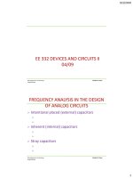
EE 332 DEVICES AND CIRCUITS II
04/09
©UW EE TC ChenMicroelectronic Circuit Design
Jaeger/Blalock
FREQUENCY ANALYSIS IN THE DESIGN
OF ANALOG CIRCUITS
Intentional placed (external) capacitors
Inherent (internal) capacitors
Stray capacitors
9/3/2010
2
©UW EE TC ChenMicroelectronic Circuit Design
Jaeger/Blalock
BJT AND ITS CAPACITIVE STRAY
(INTERNAL)
Recall diode capacitances:
Depletion capacitance:
Diffusion capacitance
©UW EE TC ChenMicroelectronic Circuit Design
Jaeger/Blalock
FREQUENCY RESPONSE OF CE SHORT-
CIRCUIT / SMALL SIGNAL MODEL
9/3/2010
3
©UW EE TC ChenMicroelectronic Circuit Design
Jaeger/Blalock
FREQUENCY RESPONSE OF CE SHORT-
CIRCUIT / SMALL SIGNAL PARAMETERS
©UW EE TC ChenMicroelectronic Circuit Design
Jaeger/Blalock
FREQUENCY RESPONSE OF CE SHORT-
CIRCUIT / GAIN
9/3/2010
4
©UW EE TC ChenMicroelectronic Circuit Design
Jaeger/Blalock
FREQUENCY RESPONSE OF CE SHORT-
CIRCUIT
Rewrite this short-circuit gain to identify the pole and
zero:
©UW EE TC ChenMicroelectronic Circuit Design
Jaeger/Blalock
FREQUENCY RESPONSE OF CE SHORT-
CIRCUIT GAIN
g
m
v
f
1
f
T
f
2
Unity gain frequency:
9/3/2010
5
©UW EE TC ChenMicroelectronic Circuit Design
Jaeger/Blalock
FREQUENCY RESPONSE OF CE SHORT-
CIRCUIT GAIN
©UW EE TC ChenMicroelectronic Circuit Design
Jaeger/Blalock
MILLER’S THEOREM
9/3/2010
6
©UW EE TC ChenMicroelectronic Circuit Design
Jaeger/Blalock
MILLER’S THEOREM
©UW EE TC ChenMicroelectronic Circuit Design
Jaeger/Blalock
EXAMPLE
Estimate the poles of the circuit.
V
DD
R
D
C
F
M
1
V
O
V
i
R
S
9/3/2010
7
©UW EE TC ChenMicroelectronic Circuit Design
Jaeger/Blalock
EXAMPLE
V
DD
R
D
C
F
M
1
V
O
V
i
R
S
ANSWER
©UW EE TC ChenMicroelectronic Circuit Design
Jaeger/Blalock
EXAMPLE
ANSWER
V
DD
R
D
C
in
M
1
V
O
V
i
R
S
C
out
9/3/2010
8
©UW EE TC ChenMicroelectronic Circuit Design
Jaeger/Blalock
EXAMPLE
ANSWER
V
DD
R
D
C
in
M
1
V
O
V
i
R
S
C
out
©UW EE TC ChenMicroelectronic Circuit Design
Jaeger/Blalock
EXAMPLE
ANSWER
V
DD
R
D
C
in
M
1
V
O
V
i
R
S
C
out
Calculate and if
=1 k and
1
, (150 ) ,
2 , 80
in out m
D S F
f f g
R k R C fF
9/3/2010
9
©UW EE TC ChenMicroelectronic Circuit Design
Jaeger/Blalock
FREQUENCY RESPONSE OF CE
AMPLIFIER
V
CC
v
i
R
2
R
1
C
1
C
2
v
o
R
s
R
C
R
E
C
E
Q1
,,
0.7 ; 0.1 ;
1(2 3904) 100; 150 ; 100 ;
1 ; 1
BE on CE sat
FA
je jc
V V V V
Q N ps V V
C pF C pF
12V
12
12
100 ; 10 ; 100 ;
10 ; 1 ; 10 ;
10 ;
s
C E L
E CC
R R k R k
R k R k R k
C C C F V
©UW EE TC ChenMicroelectronic Circuit Design
Jaeger/Blalock
FREQUENCY RESPONSE OF CE
AMPLIFIER
Three frequency regions:
Consider medium frequencies:
9/3/2010
10
©UW EE TC ChenMicroelectronic Circuit Design
Jaeger/Blalock
FREQUENCY RESPONSE OF CE
AMPLIFIER
Step 2: SS parameters
©UW EE TC ChenMicroelectronic Circuit Design
Jaeger/Blalock
FREQUENCY RESPONSE OF CE
AMPLIFIER
Step 3: Small signal analysis: Find source gain
9/3/2010
11
©UW EE TC ChenMicroelectronic Circuit Design
Jaeger/Blalock
FREQUENCY RESPONSE OF CE
AMPLIFIER
Low-Mid frequencies: include the effects of C1, C2, C
E
©UW EE TC ChenMicroelectronic Circuit Design
Jaeger/Blalock
FREQUENCY RESPONSE OF CE
AMPLIFIER
r
r
o
g
m
v
v
i
R
1
//R
2
R
s
R
L
R
C
v
o
Low-Mid frequencies: include the effects of C1, C2, C
E
Consider C2 and let C1, C
E
short
C1 C2
R
E
C
E
9/3/2010
12
©UW EE TC ChenMicroelectronic Circuit Design
Jaeger/Blalock
FREQUENCY RESPONSE OF CE
AMPLIFIER
Consider C
E
and let C1, C2 short
©UW EE TC ChenMicroelectronic Circuit Design
Jaeger/Blalock
FREQUENCY RESPONSE OF CE
AMPLIFIER
Mid-high frequencies: include the effects of C
and C
Use Miller’s Theorem to simplify the C
effects
9/3/2010
13
©UW EE TC ChenMicroelectronic Circuit Design
Jaeger/Blalock
FREQUENCY RESPONSE OF CE
AMPLIFIER
r
r
o
g
m
v
v
i
R
1
//R
2
R
L
R
C
C
C
2
C
1
©UW EE TC ChenMicroelectronic Circuit Design
Jaeger/Blalock
FREQUENCY RESPONSE OF CE
AMPLIFIER
9/3/2010
14
©UW EE TC ChenMicroelectronic Circuit Design
Jaeger/Blalock
DESIGN PROJECT
• This design project aims to utilize every single skill
you have learned in EE 332 this quarter. You will use
your newly acquired knowledge to build a useful
product that could potentially be subsequently
refined and sold.
• Your job is to simulate an audio amplifier that can
take the input from a CD player or portable music
player and amplify the signal to drive a loudspeaker.
Your design can utilize any passive electronic
components, discrete BJT’s or/and MOSFET’s (array
chips are okay too).
27
©UW EE TC ChenMicroelectronic Circuit Design
Jaeger/Blalock
DESIGN PROJECT
• Input signal specifications:
– Signal voltage: 100mV pkpk (min) – 5.6V pkpk (max)
– Signal source resistance 50 Ω
• Equipment available for testing:
– Software: PSPICE, HSPICE etc.
• Minimum Design Specifications of the amplifier:
– Output power: 0.5W (minimum)
– Load Impedance (speaker): 8Ω
– Unity Gain Bandwidth: 20Hz – 20 kHz (-3dB)
– Idling power: < 1W
– Distortion: No distortion
28
9/3/2010
15
©UW EE TC ChenMicroelectronic Circuit Design
Jaeger/Blalock
DESIGN PROJECT
• Design Description:
• A skeleton description of what your design may look like is as
follows:
• Your amplifier will take a small signal input from a music
player, and then presumably send it into a gain stage to meet
the gain requirements for the design. As you have learned, we
will need a specially designed output stage to drive a speaker
resistance of 8 ohms.
• The first is to ease requirements for simply meeting
specifications, while leaving SIGNIFICANT room for
optimization.
29
©UW EE TC ChenMicroelectronic Circuit Design
Jaeger/Blalock
DESIGN PROJECT
• Design Decision Justification:
• There is no specific topology that you should follow, the
method is open-ended and you are free to explore any
resources. With this in mind, the decisions and tradeoffs you
make in your design will be critical in determining the overall
quality of your project, and thus will play a significant role in
the final grade.
30
9/3/2010
16
©UW EE TC ChenMicroelectronic Circuit Design
Jaeger/Blalock
DESIGN PROJECT
• Design Decision Justification:
• You must justify all blocks in your design. Why did you
implement a given output stage? Which component did you
use and why? It is encouraged to meet specifications while
looking to optimize in areas performance (output power or
bandwidth). This is a great opportunity to design something
that is truly yours, so use it that way.
• Timeline:
• I anticipate that this will take about 12 hours each person of
the group to complete,
31
©UW EE TC ChenMicroelectronic Circuit Design
Jaeger/Blalock
DESIGN PROJECT
• Project Report Requirements
• Introduction
– Briefly explain the objective of the project
• Architecture Design
– Design specifications
– Block Diagrams
– Discussion on the chosen architecture
– Trade offs
• Circuit Design
– Schematics
– Design equations and calculations
– Simulation results
32
9/3/2010
17
©UW EE TC ChenMicroelectronic Circuit Design
Jaeger/Blalock
DESIGN PROJECT
• Project Report Requirements
• Results
• Maximum Output Power
– What is the largest Vpk-pk on output that is not distorted/clipping and
greater than or equal to .5W while achieving -3dB bandwidth of 20Hz-
20KHz?
• Idling power
DC power used with no input
• Grading:
• Report: Functionality: 40%; Justification: 60%
33