Sequential Verulog Topics part 10 pps
Bạn đang xem bản rút gọn của tài liệu. Xem và tải ngay bản đầy đủ của tài liệu tại đây (40.94 KB, 7 trang )
14.3 Verilog HDL Synthesis
For the purpose of logic synthesis, designs are currently written in an HDL at a
register transfer level (RTL). The term RTL is used for an HDL description style
that utilizes a combination of data flow and behavioral constructs. Logic synthesis
tools take the register transfer-level HDL description and convert it to an optimized
gate-level netlist. Verilog and VHDL are the two most popular HDLs used to
describe the functionality at the RTL level. In this chapter, we discuss RTL-based
logic synthesis with Verilog HDL. Behavioral synthesis tools that convert a
behavioral description into an RTL description are slowly evolving, but RTL-
b
ased
synthesis is currently the most popular design method. Thus, we will address only
RTL-based synthesis in this chapter.
14.3.1 Verilog Constructs
N
ot all constructs can be used when writing a description for a logic synthesis tool.
In general, any construct that is used to define a cycle-by-cycle RTL description is
acceptable to the logic synthesis tool. A list of constructs that are typically
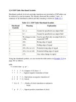
accepted by logic synthesis tools is given in Table 14-1
. The capabilities of
individual logic synthesis tools may vary. The constructs that are typically
acceptable to logic synthesis tools are also shown.
Table 14-1. Verilog HDL Constructs for Logic Synthesis
Construct
Type
Keyword or
Description
Notes
ports input, inout, output
parameters parameter
module
definition
module
signals and
variables
wire, reg, tri Vectors are allowed
instantiation module instances,
primitive gate instances
E.g., mymux m1(out, i0, i1, s); E.g.,
nand (out, a, b);
functions and
tasks
function, task Timing constructs ignored
procedural always, if, then, else, initial is not supported
case, casex, casez
procedural
blocks
begin, end, named
blocks, disable
Disabling of named blocks allowed
data flow assign Delay information is ignored
loops for, while, forever, while and forever loops must contain
@(posedge clk) or @(negedge clk)
Remember that we are providing a cycle-by-cycle RTL description of the circuit.
Hence, there are restrictions on the way these constructs are used for the logic
synthesis tool. For example, the while and forever loops must be broken by a @
(posedge clock) or @ (negedge clock) statement to enforce cycle-by-cycle
behavior and to prevent combinational feedback. Another restriction is that logic
synthesis ignores all timing delays specified by #<delay> construct. Therefore, pre-
and post-synthesis Verilog simulation results may not match. The designer must
use a description style that eliminates these mismatches. Also, the initial construct
is not supported by logic synthesis tools. Instead, the designer must use a reset
mechanism to initialize the signals in the circuit.
It is recommended that all signal widths and variable widths be explicitly specified.
Defining unsized variables can result in large, gate-level netlists because synthesis
tools can infer unnecessary logic based on the variable definition.
14.3.2 Verilog Operators
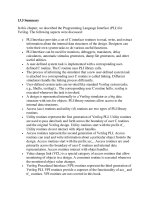
Almost all operators in Verilog are allowed for logic synthesis. Table 14-2
is a list
of the operators allowed. Only operators such as === and !== that are related to x
and z are not allowed, because equality with x and z does not have much meaning
in logic synthesis. While writing expressions, it is recommended that you use
p
arentheses to group logic the way you want it to appear. If you rely on operator
p
recedence, logic synthesis tools might produce an undesirable logic structure.
Table 14-2. Verilog HDL Operators for Logic Synthesis
Operator Type Operator Symbol Operation Performed
Arithmetic *
/
multiply
divide
+
-
%
+
-
add
subtract
modulus
unary plus
unary minus
Logical !
&&
||
logical negation
logical and
logical or
Relational >
<
>=
<=
greater than
less than
greater than or equal
less than or equal
Equality ==
!=
equality
inequality
Bit-wise ~
&
|
^
^~ or ~^
bitwise negation
bitwise and
bitwise or
bitwise ex-or
bitwise ex-nor
Reduction &
~&
|
reduction and
reduction nand
reduction or
~|
^
^~ or ~^
reduction nor
reduction ex-or
reduction ex-nor
Shift >>
<<
>>>
<<<
right shift
left shift
arithmetic right shift
arithmetic left shift
Concatenation { } concatenation
Conditional ?: conditional
14.3.3 Interpretation of a Few Verilog Constructs
Having described the basic Verilog constructs, let us try to understand how logic
synthesis tools frequently interpret these constructs and translate them to logic
gates.
The assign statement
The assign construct is the most fundamental construct used to describe
combinational logic at an RTL level. Given below is a logic expression that uses
the assign statement.
assign out = (a & b) | c;
This will frequently translate to the following gate-level representation:
If a, b, c, and out are 2-bit vectors [1:0], then the above assign statement will
frequently translate to two identical circuits for each bit.
If arithmetic operators are used, each arithmetic operator is implemented in terms
of arithmetic hardware blocks available to the logic synthesis tool. A 1-bit full
adder is implemented below.
assign {c_out, sum} = a + b + c_in;
Assuming that the 1-bit full adder is available internally in the logic synthesis tool,
the above assign statement is often interpreted by logic synthesis tools as follows:
If a multiple-bit adder is synthesized, the synthesis tool will perform optimization
and the designer might get a result that looks different from the above figure.
If a conditional operator ? is used, a multiplexer circuit is inferred.
assign out = (s) ? i1 : i0;
It frequently translates to the gate-level representation shown in Figure 14-3
.
Figure 14-3. Multiplexer Description
The if-else statement
Single if-else statements translate to multiplexers where the control signal is the
signal or variable in the if clause.
if(s)
out = i1;
else
out = i0;
The above statement will frequently translate to the gate-level description shown in
Figure 14-3
. In general, multiple if-else-if statements do not synthesize to large
multiplexers.
The case statement
The case statement also can used to infer multiplexers. The above multiplexer
would have been inferred from the following description that uses case statements:
case (s)
1'b0 : out = i0;
1'b1 : out = i1;
endcase
Large case statements may be used to infer large multiplexers.
for loops
The for loops can be used to build cascaded combinational logic. For example, the
following for loop builds an 8-bit full adder:
c = c_in;
for(i=0; i <=7; i = i + 1)
{c, sum[i]} = a[i] + b[i] + c; // builds an 8-bit ripple adder
c_out = c;
The always statement
The always statement can be used to infer sequential and combinational logic. For
sequential logic, the always statement must be controlled by the change in the
value of a clock signal clk.
always @(posedge clk)
q <= d;
This is inferred as a positive edge-triggered D-flipflop with d as input, q as output,
and clk as the clocking signal.
Similarly, the following Verilog description creates a level-sensitive latch:
always @(clk or d)
if (clk)
q <= d;
For combinational logic, the always statement must be triggered by a signal other
than the clk, reset, or preset. For example, the following block will be interpreted
as a 1-bit full adder:
always @(a or b or c_in)
{c_out, sum} = a + b + c_in;
The function statement
Functions synthesize to combinational blocks with one output variable. The output
might be scalar or vector. A 4-bit full adder is implemented as a function in the
Verilog description below. The most significant bit of the function is used for the
carry bit.
function [4:0] fulladd;
input [3:0] a, b;
input c_in;
begin
fulladd = a + b + c_in; //bit 4 of fulladd for carry, bits[3:0] for sum.
end
endfunction