Tài liệu môn vật liệu nano và mảng mỏng
Bạn đang xem bản rút gọn của tài liệu. Xem và tải ngay bản đầy đủ của tài liệu tại đây (2.54 MB, 41 trang )
Phase change memory technology
Geoffrey W. Burr, Matthew J. Breitwisch, Michele Franceschini, Davide Garetto, Kailash Gopalakrishnan, Bryan
Jackson, Bülent Kurdi, Chung Lam, Luis A. Lastras, Alvaro Padilla, Bipin Rajendran, Simone Raoux, and Rohit
S. Shenoy
Citation: Journal of Vacuum Science & Technology B 28, 223 (2010); doi: 10.1116/1.3301579
View online: />View Table of Contents: />
cu
u
du
o
ng
th
an
co
ng
.c
om
Published by the AVS: Science & Technology of Materials, Interfaces, and Processing
Redistribution subject to AVS license or copyright; see Download to IP: 86.31.48.42 On: Mon, 17 Mar 2014 09:16:29
CuuDuongThanCong.com
/>
REVIEW ARTICLE
Phase change memory technology
Geoffrey W. Burra͒
IBM Almaden Research Center, 650 Harry Road, San Jose, California 95120
Matthew J. Breitwisch and Michele Franceschini
IBM T.J. Watson Research Center, Yorktown Heights, New York 10598
Davide Garetto, Kailash Gopalakrishnan, Bryan Jackson, and Bülent Kurdi
IBM Almaden Research Center, 650 Harry Road, San Jose, California 95120
Chung Lam and Luis A. Lastras
IBM T.J. Watson Research Center, Yorktown Heights, New York 10598
Alvaro Padilla and Bipin Rajendran
Simone Raoux
IBM T.J. Watson Research Center, Yorktown Heights, New York 10598
Rohit S. Shenoy
.c
om
IBM Almaden Research Center, 650 Harry Road, San Jose, California 95120
IBM Almaden Research Center, 650 Harry Road, San Jose, California 95120
ng
͑Received 4 January 2010; accepted 4 January 2010; published 19 March 2010͒
cu
u
du
o
ng
th
an
co
The authors survey the current state of phase change memory ͑PCM͒, a nonvolatile solid-state
memory technology built around the large electrical contrast between the highly resistive amorphous
and highly conductive crystalline states in so-called phase change materials. PCM technology has
made rapid progress in a short time, having passed older technologies in terms of both sophisticated
demonstrations of scaling to small device dimensions, as well as integrated large-array
demonstrators with impressive retention, endurance, performance, and yield characteristics. They
introduce the physics behind PCM technology, assess how its characteristics match up with various
potential applications across the memory-storage hierarchy, and discuss its strengths including
scalability and rapid switching speed. Challenges for the technology are addressed, including the
design of PCM cells for low reset current, the need to control device-to-device variability, and
undesirable changes in the phase change material that can be induced by the fabrication procedure.
They then turn to issues related to operation of PCM devices, including retention, device-to-device
thermal cross-talk, endurance, and bias-polarity effects. Several factors that can be expected to
enhance PCM in the future are addressed, including multilevel cell technology for PCM ͑which
offers higher density through the use of intermediate resistance states͒, the role of coding, and
possible routes to an ultrahigh-density PCM technology. © 2010 American Vacuum Society.
͓DOI: 10.1116/1.3301579͔
I. MOTIVATION FOR PHASE CHANGE MEMORY
A. Case for a next-generation memory
As with many modern technologies, the extent to which
nonvolatile memory ͑NVM͒ has pervaded our day-to-day
lives is truly remarkable. From the music on our MP3 players, to the photographs on digital cameras, the stored e-mail
and text messages on smart phones, the documents we carry
on our USB thumb drives, and the program code that enables
everything from our portable electronics to cars, the NVM
known as Flash memory is everywhere around us. Both NOR
and NAND Flash began humbly enough, as unappreciated
a͒
Electronic mail:
223
J. Vac. Sci. Technol. B 28„2…, Mar/Apr 2010
side projects of a Toshiba DRAM engineer named Masuoka.1
However, from his basic patents in 1980 and 1987,1 Flash
has grown in less than 3 decades to become a $20 billion/
year titan of the semiconductor industry.2,3
This market growth has been made possible by tremendous increases in the system functionality ͑e.g., more gigabytes͒ that can be delivered in the same size package.
These improvements are both a byproduct of and the driving
force for the relentless march to smaller device dimensions
known as Moore’s law.4 The history of the solid-state
memory industry, and of the semiconductor industry as a
whole, has been dominated by this concept: Higher densities
at similar cost lead to more functionality, and thus more applications, which then spur investment for the additional re-
1071-1023/2010/28„2…/223/40/$30.00
©2010 American Vacuum Society
223
Redistribution subject to AVS license or copyright; see Download to IP: 86.31.48.42 On: Mon, 17 Mar 2014 09:16:29
CuuDuongThanCong.com
/>
Burr et al.: Phase change memory technology
224
ng
.c
om
sional scaling, leading Flash researchers to explore even
more complicated schemes for FinFET Flash devices21,22 or
three-dimensional ͑3D͒ stacking of Flash memory.23–26
With these difficulties in scaling to future technology
nodes, Flash researchers are already hard pressed to maintain
specifications, such as write endurance, retention of heavily
cycled cells, and write/erase performance, let alone improve
them. As one indication of these pressures, some authors
have pointed out that in cases such as digital photography,
larger capacity formats can be expected to be tolerant of even
more relaxed endurance specifications.20 However, at the
same time that Flash is struggling to maintain current levels
of reliability and performance while increasing density, new
applications are opening up for which these specifications
are just barely adequate.
The solid-state drive ͑SSD͒ market—long dominated by
high-cost, battery-backed DRAM for military and other critical applications—has grown rapidly since the introduction of
Flash-based SSD drives, passing $400 million in revenues in
2007.27 One reason for the time delay between the widespread use of Flash in consumer applications and its appearance in SSD applications was the need to build system controllers that could hide the weaknesses of Flash. Consider
that each underlying block of Flash devices takes over a
millisecond to erase, and if written to continuously, would
start to exhibit significant device failures in mere seconds.
Sophisticated algorithms have been developed to avoid unnecessary writes, to perform static or dynamic wear leveling,
to pipeline writes, and to maintain pre-erased blocks in order
to finesse or hide the poor write/erase performance.28,29 Together with simple overprovisioning of extra capacity, these
techniques allow impressive system performance. For instance, the Texas Memory Systems RamSan-500 can write at
2 Gbytes/s with an effective Flash endurance of
Ͼ15 years.30 However, it is interesting to note that despite
the fact that MLC Flash costs much less than 1 bit/cell
single-layer cell ͑SLC͒ Flash, for a long time only SLC Flash
was used in SSD devices.30 This is because MLC Flash tends
to have ten times lower endurance and two times lower write
speed than SLC Flash,30 illustrating the importance of these
specifications within SSD applications.
Thus there is a need for a new next-generation NVM that
might have an easier scaling path than NAND Flash to reach
the higher densities offered by future technology nodes. Simultaneously, there is a need for a memory that could offer
better write endurance and input-output ͑I/O͒ performance
than Flash, in order to bring down the cost while increasing
the performance of NVM-based SSD drives. However the
size of the opportunity here is even larger: The emergence of
a nonvolatile solid-state memory technology that could combine high performance, high density, and low cost could
usher in seminal changes in the memory/storage hierarchy
throughout all computing platforms, ranging all the way up
to high-performance computing. If the cost per bit could be
driven low enough through ultrahigh memory density, ultimately such a storage-class memory ͑SCM͒ device could po-
cu
u
du
o
ng
th
an
search and development needed to implement the “next size
smaller” device. Throughout this extensive history, extrapolation from the recent past has proven to be amazingly reliable for predicting near-future developments. Thus the
memory products that will be built in the next several years
have long been forecast.5
Beyond the near future, however, while the planned device sizes may be sketched out, for the first time in many
years it is not clear exactly how achievable these goals might
be. This uncertainty is present in many portions of the semiconductor industry, primarily due to the increasing importance of device-to-device variations, and to the common dependence on continued lithographic innovation. New
patterning techniques will almost certainly be needed to replace the 193 nm immersion and “double patterning” techniques now being used to implement the 32 nm and even 22
nm nodes.6,7 In addition to such issues common to the larger
semiconductor industry, however, the Flash industry faces
additional uncertainties specific to its technology.
Over the past few years, Flash has been wrestling with
unpleasant tradeoffs between the scaling of lateral device
dimensions, the need to maintain coupling between the control and floating gates, the stress-induced leakage current
͑SILC͒ that is incurred by programming with large voltages
across ultrathin oxides, and the cell-to-cell parasitic interference between the stored charges in closely packed cells.3,8–10
Many alternative cell designs were proposed, typically involving replacement of the floating polysilicon gate by some
type of charge-trapping layer, such as the silicon nitride at
the center of the silicon-oxide-nitride-oxide-semiconductor
͑SONOS͒ cell structure.11 While early SONOS memory devices used extremely thin tunnel and blocking oxides for
acceptable write/erase performance, and thus suffered from
data retention issues,12 recent work seems to have migrated
to tantalum nitride-alumina-nitride-oxide-semiconductor
͑TANOS͒ structures.13–16 These structures offer improved
immunity to both SILC and parasitic interference between
cells,16 while also allowing any defects to gracefully degrade
signal-to-noise ratio rather than serve as avenues for catastrophic charge leakage.9,16 TANOS data retention has improved to acceptable levels,9 and the reduced programming
efficiency is now understood.16
However, TANOS structures cannot help to scale NOR
Flash, because the charge injected at one edge of such devices by channel hot-electron injection17 must be redistributed throughout the floating gate after programming.10 For
NAND Flash, the finite and fairly modest number of discrete
traps in each TANOS cell have accelerated the onset of new
problems, ranging from device-to-device variations in Vt,9
stochastic or “shot-noise” effects,9 random telegraph
noise,18,19 and a significant reduction in the number of stored
electrons that differentiate one stored analog level from the
next.20 These issues are particularly problematic for multilevel cell ͑MLC͒ Flash, where multiple analog levels allow
an increase in the effective number of bits per physical device by a factor of 2, 3, or even 4. Worse yet, such fewelectron problems will only increase with further dimen-
co
224
J. Vac. Sci. Technol. B, Vol. 28, No. 2, Mar/Apr 2010
Redistribution subject to AVS license or copyright; see Download to IP: 86.31.48.42 On: Mon, 17 Mar 2014 09:16:29
CuuDuongThanCong.com
/>
Burr et al.: Phase change memory technology
225
FIG. 1. ͑Color online͒ Programming of a PCM device involves application
of electrical power through applied voltage, leading to internal temperature
changes that either melt and then rapidly quench a volume of amorphous
material ͑reset͒, or which hold this volume at a slightly lower temperature
for sufficient time for recrystallization ͑set͒. A low voltage is used to sense
the device resistance ͑read͒ so that the device state is not perturbed.
ng
.c
om
materials.32 The amorphous phase tends to have high electrical resistivity, while the crystalline phase exhibits a low resistivity, sometimes three or four orders of magnitude lower.
Due to this large resistance contrast, the change in read current is quite large, opening up the opportunity for the multiple analog levels needed for MLC operations.32
To set the cell into its low-resistance state, an electrical
pulse is applied to heat a significant portion of the cell above
the crystallization temperature of the phase change material.
This set operation tends to dictate the write speed performance of PCM technology, since the required duration of
this pulse depends on the crystallization speed of the phase
change material ͑Sec. II B͒. Set pulses shorter than 10 ns
have been demonstrated.33–36 Because the crystallization process is many orders of magnitude slower at low temperatures
͑Ͻ120 ° C͒, PCM is a NVM technology that can offer years
of data lifetime.
In the reset operation, a larger electrical current is applied
in order to melt the central portion of the cell. If this pulse is
cutoff abruptly enough, the molten material quenches into
the amorphous phase, producing a cell in the high-resistance
state. The reset operation tends to be fairly current and power
hungry, and thus care must be taken to choose an access
device capable of delivering high current and power without
requiring a significantly larger footprint than the PCM element itself. The read operation is performed by measuring
the device resistance at low voltage so that the device state is
not perturbed. These operations are summarized in Fig. 1.
Even though the principle of applying phase change materials to electronic memory was demonstrated as long ago as
the 1960s,37 interest in PCM was slow to develop compared
to other NVM candidates. However, renewed interest in
PCM technology was triggered by the discovery of fast
͑Ͻ100 ns͒ crystallizing materials such as Ge2Sb2Te5 ͑GST͒
or Ag- and In-doped Sb2Te ͑AIST͒ ͑Refs. 38 and 39͒ by
optical storage researchers. Over the past few years, a large
number of sophisticated integration efforts have been undertaken in PCM technology, leading to demonstration of high
endurance,40 fast speed,41 inherent scaling of the phase
change process out beyond the 22 nm node,42 and integration
at technology nodes down to 90 nm.43 One important remaining unknown for the success of PCM technology is
cu
u
du
o
ng
th
an
tentially displace magnetic hard-disk drives ͑HDD͒ in enterprise storage server systems.
Fortunately, new NVM candidate technologies have been
under consideration as possible Flash “replacements” for
more than a decade.31 These candidates range from technologies that have reached the marketplace after successful integration in real complementary metal oxide semiconductor
͑CMOS͒ fabs ͓ferroelectric ͑FeRAM͒ and magnetic
͑MRAM͒ random access memory ͑RAM͔͒, to novel ideas
that are barely past the proof-of-principle stage ͑racetrack
memory and organic RAM͒, to technologies that are somewhere in between ͓phase change memory ͑PCM͒, resistance
RAM, and solid-electrolyte memory͔.31 Each of these has its
strengths and weaknesses. In general, the farther along a
technology has progressed toward real integration, the more
that is known about it. Moreover, as research gives way to
development, it is typically new weaknesses—previously
hidden yet all too quickly considered to be obvious in
hindsight—that tend to be revealed. In contrast, by avoiding
these known pitfalls, fresh new technologies are immediately
attractive, at least until their own unique weaknesses are
discovered.
In this article, we survey the current state of PCM. This
technology has made rapid progress in a short time, having
passed older technologies such as FeRAM and MRAM in
terms of sophisticated demonstrations of scaling to small device dimensions. In addition, integrated large-array demonstrators with impressive retention, endurance, performance,
and yield characteristics31 have been built.
The article is organized into seven sections, beginning
with the current section titled “Motivation for PCM.” Section
I also includes a brief overview of PCM technology and an
assessment of how its characteristics match up with various
potential applications across the memory-storage hierarchy.
Section II goes into the physics behind PCM in more depth,
in terms of the underlying phase change materials and their
inherent scalability, and the physical processes affecting the
switching speed of PCM devices. The section concludes with
a survey of PCM modeling efforts published to date, and a
discussion of scalability as revealed by ultrasmall prototype
PCM devices.
In Sec. III, we address factors that affect the design and
fabrication of PCM devices, including cell design, variability, changes in the phase change material induced by the
fabrication procedure, and the design of surrounding access
circuitry. We then turn to issues related to operation of PCM
devices in Sec. IV, including endurance, retention, and
device-to-device cross-talk. Section V addresses several factors that can be expected to enhance PCM in the future,
including multilevel cell technology for PCM, the role of
coding, and possible routes to an ultrahigh-density PCM
technology. The conclusion section ͑Sec. VI͒ is followed by
a brief acknowledgments section.
co
225
B. What is PCM?
PCM exploits the large resistance contrast between the
amorphous and crystalline states in so-called phase change
JVST B - Microelectronics and Nanometer Structures
Redistribution subject to AVS license or copyright; see Download to IP: 86.31.48.42 On: Mon, 17 Mar 2014 09:16:29
CuuDuongThanCong.com
/>
Burr et al.: Phase change memory technology
226
.c
om
FIG. 2. ͑Color online͒ Memory hierarchy in computers spans orders of magnitude in read-write performance, ranging from small amounts of expensive
yet high-performance memory sitting near the CPU to vast amounts of low
cost yet very slow off-line storage.
ng
ing memory hierarchy for modern computers. This memory
hierarchy, shown in Fig. 2, is designed to bridge the performance gap between the fast central processing units and the
slower ͑sometimes much slower͒ memory and storage technologies, while keeping overall system costs down. Figure 3
shows how PCM is expected to compare to the four major
incumbent memory and storage technologies in terms of cost
and performance. The enormous range of cost and performance spanned by these technologies makes a single universal memory—one capable of replacing all of these wellestablished memory and storage techniques—an aggressive
goal indeed.
However, Fig. 4 shows that there is currently a gap of
more than three orders of magnitude between the access time
of off-chip dynamic random access memory ͑DRAM͒ ͑60
cu
u
du
o
ng
th
an
whether the memory access device ͑diode,43 transistor,44 etc.͒
in a dense memory array will be able to supply sufficient
current to reset the PCM cell. Already, in order to try to
minimize the reset current, it is assumed that the dimension
of the phase change material will be only 30% of the lithographic feature size F,5 mandating the use of sublithographic
techniques for accurate definition of this critical dimension
͑CD͒. However, even with this difficult integration task, the
success of PCM technology may end up depending on advances in the access device as much as on the PCM cell
itself.5
Important device characteristics for a PCM cell include
widely separated set and reset resistance distributions ͑necessary for sufficient noise margin upon fast readout͒, the
ability to switch between these two states with accessible
electrical pulses, the ability to read/sense the resistance states
without perturbing them, high endurance ͑allowing many
switching cycles between set and reset͒, long data retention
͑usually specified as 10 year data lifetime at some elevated
temperature͒, and fast set speed ͑the time required to recrystallize the cell from the reset state͒. Data retention usually
comes down to the cell’s ability to retain the amorphous reset
state by avoiding unintended recrystallization. An additional
aspect that can be of significant importance is the ability to
store ͑and retain over time͒ more than 1 bit of data per cell
since this allows one to increase effective density much like
MLC Flash without decreasing the feature size.
A critical property of phase change materials is the socalled threshold switching.45–48 Without this effect PCM
would simply not be a feasible technology because in the
high resistance-state, extremely high voltages would be required to deliver enough power to the cell to heat it above
the crystallization temperature. However, when a voltage
above a particular threshold Vt is applied to a phase change
material in the amorphous phase, the resulting large electrical fields greatly increase the electrical conductivity. This
effect is still not completely understood but is attributed to a
complex interplay between trapped charge, device current,
and local electrical fields.45,49 With the previously resistive
material now suddenly highly conducting, a large current
flows—which can then heat the material. However, if this
current pulse is switched off immediately after the threshold
switching, the material returns to the highly resistive amorphous phase after about 30 ns,50 with both the original
threshold voltage Vt and reset resistance recovering slowly
over time.50,51 Only when a current sufficient to heat the
material above the crystallization temperature, but below the
melting point, is sustained for a long enough time does the
cell switch to the crystalline state. The threshold switching
effect serves to make this possible with applied voltages of a
few volts, despite the high initial resistance of the device in
the reset state.
co
226
C. Potential applications of PCM
The ultimate goal of researchers and developers studying
emerging memory technologies is to devise a universal
memory that could work across multiple layers of the exist-
FIG. 3. ͑Color online͒ Qualitative representation of the cost and performance
of various memories and storage technologies, ranging from extremely
dense yet slow HDDs to ultrafast but expensive SRAM. F is the size of the
smallest lithographic feature. A smaller device footprint leads to higher density and thus lower cost.
J. Vac. Sci. Technol. B, Vol. 28, No. 2, Mar/Apr 2010
Redistribution subject to AVS license or copyright; see Download to IP: 86.31.48.42 On: Mon, 17 Mar 2014 09:16:29
CuuDuongThanCong.com
/>
Burr et al.: Phase change memory technology
227
cu
u
du
o
ng
th
.c
om
an
ns͒ and the write-cycle time of Flash ͑1 ms͒. To set this into
human perspective, this slow write-cycle time is equivalent
to a person, who might be making data-based decisions
analogous to a single central processor unit ͑CPU͒ operation
every second, having to wait approximately 10 days to
record a small block of information. An interesting region on
this chart sits just above off-chip DRAM, where access times
of 100–1000 ns could potentially be enabled by a “Storage
Class Memory ͑SCM͒” made possible by PCM.
In the remainder of this section, we examine the suitability of PCM for the layers of the memory hierarchy currently
served by static random access memory ͑SRAM͒, DRAM
͑dynamic͒, and NOR and NAND Flash. We also discuss the
emerging area of storage-class memory, for which Flashbased solid-state drives are just now becoming available.
While the two principal integration metric are cost and performance, we also briefly examine critical reliability issues
such as data retention and read/write endurance here ͑leaving
more in-depth discussion to Sec. IV͒. We do not consider the
relative merit of power consumption, assuming instead that
all these technologies are roughly comparable within an order of magnitude. The nonvolatility of PCM does compare
favorably to volatile memories, both in terms of standby
power as well as by enabling easier recovery from system or
power failures in critical applications.
ng
FIG. 4. ͑Color online͒ Access times for various storage and memory technologies, both in nanoseconds and in terms of human perspective. For the
latter, all times are scaled by 109 so that the fundamental unit of a single
CPU operation is analogous to a human making a 1 s decision. In this
context, writing data to Flash memory can require more than “1 week” and
obtaining data from an offline tape cartridge takes “1000 years” ͑Refs. 29
and 55͒.
sistors, two positive metal oxide semiconductor field effect
transistors and four negative metal oxide semiconductor field
effect transistors, and thus occupies more than 120F2 in chip
real estate per bit. ͑Here F is the size of the smallest lithographic feature, so that this measure of device size is independent of the particular device technology used to fabricate
the memory.͒ Embedded SRAM typically runs at the CPU
clock speed, thus access times for these devices must be less
than 10 ns. Commodity SRAM used in cell phones runs at
slower clock speeds, allowing access times in the tens of
nanoseconds.
While there is no problem for PCM to improve upon the
large SRAM cell size, even if a large access device is used
for the PCM cell, SRAM performance is hard to match. The
performance limiter for PCM is the set speed, which in turn
depends on the crystallization speed of the phase change material. As will be described in detail in Sec. II B, while some
researchers demonstrated the use of set pulses shorter than
10 ns,33–36 most of the realistically large array demonstrations tend to use set pulses that range from roughly 50
to 500 ns in length.52
In any case, the most stringent requirement for any
emerging memory technology that seeks to replace SRAM is
endurance. For all practical purposes, the read/write endurance of SRAM is infinite. While read endurance is not a
likely problem for PCM, the required write endurance for
SRAM replacement is probably 1018—out of reach for nearly
all NVM technologies. Storing data semipermanently with
PCM and most other NVM technologies involves some form
of “brute force” that alters an easily observable material
characteristic of the memory device. For PCM, this brute
force is the melt-quench reset operation, and at such elevated
temperatures, it has been shown that the constituent atoms of
a phase change material will tend to migrate over time,40,53
as discussed in Secs. IV C and IV D.
Since nonvolatility is not a requirement for SRAM applications, one might be able to trade some data retention for
improved endurance. Some remote evidence of this trade-off
has been demonstrated by showing a strong correlation between the total energy in the reset pulse and the resulting
PCM endurance.40 The best case endurance, achieved for the
lowest-energy reset pulses, was 1012 set-reset cycles.40 Yet
this is still six orders of magnitude away from the target
specification for SRAM.
co
227
1. PCM as SRAM
Much of the SRAM used in computers today is embedded
close to the CPU, serving as high-performance level 1 ͑L1͒
and level 2 ͑L2͒ cache memories. Some off-chip level 3 ͑L3͒
cache memories also use SRAM. In consumer electronics,
SRAM has been used in combination with NOR Flash in cell
phones. A typical SRAM cell comprises of six CMOS tran-
2. PCM as DRAM
DRAM is used in a more diversified set of applications
than SRAM. Most of the characteristics discussed in Sec.
I C 1 for the replacement of SRAM also apply to the replacement of DRAM, although in most cases the specifications are
slightly relaxed. Access times of tens of nanoseconds would
be acceptable for most computer and consumer electronics
applications of DRAM. For embedded DRAM used as video
RAM and L3 cache,54 however, an access time of 10 ns or
less is required. As for write endurance, the requirement can
be estimated using the following equation:55
JVST B - Microelectronics and Nanometer Structures
Redistribution subject to AVS license or copyright; see Download to IP: 86.31.48.42 On: Mon, 17 Mar 2014 09:16:29
CuuDuongThanCong.com
/>
Burr et al.: Phase change memory technology
͑1͒
cu
u
du
o
ng
th
an
where E is endurance, Tlife is the life expectancy of the system, B is the memory bandwidth, ␣ is the wear-leveling efficiency, and C is the system memory capacity. Assuming a
typical server with a 10 year life expectancy, 1 Gbyte/s bandwidth, 10% wear-leveling efficiency, and 16 Gbyte capacity,
the endurance requirement is approximately 2 ϫ 108—well
within the reach of PCM.44,56
There is also a power argument to be made when discussing PCM as a potential DRAM replacement. This might
seem to be a difficult case to make for a technology for
which every write cycle involves heating to temperatures
ranging from 400 to 700 ° C. However, DRAM turns out to
be a fairly power-hungry technology. This is not due to its
periodic refresh, however, which takes place only infrequently, and is not too strongly related to the underlying
physical storage mechanism of charging up a local capacitor.
Instead, power inefficiency in DRAM is due to the simultaneous addressing of multiple banks within the chip. For every bit that passes into or out of a DRAM chip, 8 or even 16
devices are being internally accessed ͑read and then rewritten͒, somewhat as if your librarian knocked an entire row of
books onto the floor each time you asked for a book. Lowpower DRAM intended for mobile, battery-powered applications tends to have lower performance, although some developments have been made that can combine high performance
with low power.57 However, the inherent need to rewrite after each read access is unavoidable for a volatile memory
such as DRAM. Thus simply by being nonvolatile, PCM
could potentially offer a lower-power alternative to DRAM,
despite the inherently power-hungry nature of PCM write
operations.
For standalone memories, cost is directly proportional to
memory cell size. State of the art DRAM cells occupy 6F2 in
chip area. Thus for PCM to compete in the DRAM arena,
PCM cell size would need to be this size or smaller with
comparable “array efficiency” ͑the fraction of the chip area
dedicated to memory devices rather than to peripheral circuitry͒. Fortunately, such small cell sizes have already been
demonstrated using a diode select device.56 PCM also competes favorably with DRAM in terms of forward scaling into
future generations, as DRAM developers are quickly hitting
various scaling limits associated with storage interference,
device leakage, and challenges in integrating high aspectratio capacitors in tight spaces. Currently, DRAM has fallen
behind NAND Flash and standard CMOS logic technologies
in terms of scaling to the 45 nm technology node and preparation for the 32 nm node. However, DRAM is a proven,
reliable technology that has been employed in modern computers since the early 1970s. It would be a long journey to
displace such a stable technology.
a two-dimensional array is directly connected to its wordand bit-line input lines ͑with the source electrode of each cell
sharing a common ground͒, whereas in NAND memory architectures, small blocks of cells are connected in series between a high input signal and ground. Thus, while NAND
flash can inherently be packed more densely ͑due to its
smaller unit cell size͒ than NOR flash, NOR flash offers significantly faster random access ͑since each cell in the array is
directly connected to the input lines͒. However, since NOR
memory requires large programming currents ͑to place
charge on the floating gate via channel hot electrons͒, its
programming throughput ͑measured in MB/s͒ is much
slower than that of the block-based NAND memory architectures ͑which, by utilizing the Fowler–Nordheim tunneling,
can utilize lower programming currents that permit many
bits to be processed in parallel͒.58 As a consequence, NOR
memory offers significantly faster random access with low
programming throughput, and thus is mainly used for applications such as embedded logic that require fast access to
data that is modified only occasionally. In contrast, NAND
memory is a high-density, block-based architecture with
slower random access, which is mainly used for mass storage
applications.
NOR Flash memory cells occupy about 10F2, with an access time upon read of a few tens of nanoseconds or more.
However, the access time upon write for NOR Flash is typically around 10 s, and the write/erase endurance ͑for both
NOR as well as NAND͒ is only 100 000 cycles. These characteristics are well within the capabilities of current PCMs.
NOR Flash with its floating gate technology has difficulties
scaling below 45 nm, mainly due to difficulties in scaling the
thickness of the tunnel oxide. It is thus no surprise that NOR
Flash is the popular target for first replacement by most PCM
developers.
NAND Flash, on the other hand, is a much harder target
despite PCM’s superiority in both endurance and read performance. Cost is the biggest challenge. A NAND Flash
memory cell occupies only 4F2 of chip area, and as discussed earlier, NAND will be able to maintain this through at
least 22 nm using trap storage technology13 and possibly
three-dimensional integration.26 Furthermore, MLC NAND
has been shipping 2 bits per physical memory cell for years,
and is promising to increase this to 4 bits per cell.59
NAND Flash is mainly used in consumer electronic devices, where cost is the paramount concern, and in the
emerging SSD market to replace magnetic HDDs, where
both cost and reliability are important. The prerequisites for
PCM to replace NAND Flash are 4F2 memory cell size, at
least 2 bit MLC capability, and three-dimensional integration
to further increase the effective number of bits per unit area
of underlying silicon. A 4F2 cell dictates a memory element
that can be vertically stacked over the select device, as
shown in Fig. 5. Multilevel storage seems to be within reach
of PCM given its inherently wide resistance range, and both
2 and 4 bits per cell have already been demonstrated in
small-scale demonstrations.60,61 Even though write operations are slow for NAND Flash, it tends to achieve an impres-
.c
om
B
,
␣C
ng
E = Tlife
228
co
228
3. PCM as Flash
There are two kinds of Flash memories, NOR and NAND.
In ͑common-source͒ NOR memory architectures, each cell in
J. Vac. Sci. Technol. B, Vol. 28, No. 2, Mar/Apr 2010
Redistribution subject to AVS license or copyright; see Download to IP: 86.31.48.42 On: Mon, 17 Mar 2014 09:16:29
CuuDuongThanCong.com
/>
229
Burr et al.: Phase change memory technology
229
could potentially allow the total amount of DRAM required
to maintain ultrahigh bandwidth to be greatly reduced, thus
reducing overall system cost and power.
II. PHYSICS OF PCM
A. Phase change materials and scalability
4. PCM as storage-class memory
cu
u
du
o
ng
th
an
In addition to the established segments of the memory
hierarchy we have described ͑SRAM, DRAM, and Flash͒,
the gap in access times between 1 ms and 100 ns shown in
Fig. 4 opens up the possibility of SCM.28,29 SCM would blur
the traditional boundaries between storage and memory by
combining the benefits of a solid-state memory, such as high
performance and robustness, with the archival capabilities
and low cost of conventional hard-disk magnetic storage.
Such a technology would require a solid-state nonvolatile
memory that could be manufactured at an extremely high
effective areal density, using some combination of sublithographic patterning techniques, multiple bits per cell, and
multiple layers of devices ͑Sec. V C͒. The target density
probably needs to exceed current MLC NAND Flash densities
by a factor of 2–8 times in order to bring the cost of SCM
down close to the cost of reliable enterprise HDD.
The opportunity for SCM itself actually breaks into two
segments. The slower variant, referred to as S-class SCM,29
would act much like a Flash-based SSD except with better
native endurance and write performance. Here access times
of 1 – 3 s would be acceptable, but low cost via high density would be of paramount importance. The other variant,
referred to as M-class SCM,29 requires access times of 300
ns or less, with both cost and power as considerations. This
threshold of 300 ns is considered to be the point at which an
M-class SCM would be fast enough to be synchronous with
memory operations, so that it could be connected to the usual
memory controller.29 In contrast, S-class SCM, SSD, and
HDD would all be accessed through an I/O controller for
asynchronous access. M-class SCM would likely not be as
fast as main memory DRAM. However, by being nonvolatile, lower in power per unit capacity ͑via high density͒, and
lower in cost per capacity, the presence of M-class SCM
co
ng
sive write data rate because its low write power allows for
programming of many bits in parallel. Thus to deliver equal
or better write bandwidth, PCM developers will need to
work on reducing the write power so that the data bus can be
as wide as possible.
.c
om
FIG. 5. ͑Color online͒ Semiconductor device technology node is commonly
described by the minimum feature size F that is available via lithographic
patterning. Thus the smallest device area that can be envisioned which is
still accessible by lithographically defined wiring is 4F2. To increase effective bit density beyond this, either sublithographic wiring, multiple bits per
device ͑analogous to MLC Flash technology͒, or multiple layers of stacked
memory arrays are required, as described in Sec. V C.
As discussed in Sec. I, the NVM industry faces the prospect of a costly and risky switch from a known and established technology ͑Flash͒ into something much less well
known ͑either PCM or something else͒. Understandably, the
industry wants to make such leaps rare.
The problem here is not that one might fail to create a
successful first product. That would be unpleasant but not
devastating, because this would happen during the early development stage, where the level of investment is small and
multiple alternative approaches are still being pursued. Instead, the nightmare scaling scenario is one in which the new
technology works perfectly well for the first generation, yet
is doomed to failure immediately afterward. If only one or
two device generations succeed, then the NVM industry,
having just invested heavily into this new technology, will be
forced to make yet another switch and start the learning process all over again.
Thus scaling studies are designed to look far down the
device roadmap, to try to uncover the showstoppers that
might bedevil a potential NVM technology at sizes much
smaller than what can be built today. In the case of PCM
technology, two aspects of scalability need to be considered:
the scaling properties of the phase change materials and the
scaling properties of PCM devices. In this section, we survey
recent literature covering both of these considerations. In
general, experiments have shown that PCM is a very promising technology with respect to scalability.
It is well known that the properties of nanoscale materials
can deviate from those of the bulk material, and can furthermore be a strong function of size. For example, it is typical
for nanoparticles to have a lower melting temperature than
bulk material of the same chemical composition, because the
ratio of surface atoms to volume atoms is greatly increased.
A recurring theme in such studies is the larger role that surfaces and interfaces play as dimensions are reduced.
Phase change material parameters that are significant for
PCM applications—and the device performance properties
that are influenced by these parameters—are summarized in
Table I. For optical applications the change in optical constants as a function of film thickness is also important, but
for this article we restrict our considerations to material parameters relevant to electronic memory applications. As can
be seen from Table I, there is a large set of material parameters that influence the PCM device, either affecting one of
the two writing operations ͑set to low resistance; reset to
high resistance͒ or the read operation.
A particularly important phase change material parameter
is the crystallization temperature, Tx. This is not necessarily
the temperature at which crystallization is most likely, but
instead is the lowest temperature at which the crystallization
JVST B - Microelectronics and Nanometer Structures
Redistribution subject to AVS license or copyright; see Download to IP: 86.31.48.42 On: Mon, 17 Mar 2014 09:16:29
CuuDuongThanCong.com
/>
230
Burr et al.: Phase change memory technology
230
TABLE I. Some phase change material parameters and the device performance characteristics they influence.
Phase change material parameter
Influence on PCM device performance
Crystallization temperature and thermal stability
of the amorphous phase
Data retention and archival lifetime
Set power
Reset power
On/off ratio
Set and reset current
Set voltage and reading voltage
Set and reset power
Set pulse duration ͑and thus power͒
Data rate
Reset pulse duration ͑and thus power͒
Melting temperature
Resistivity in amorphous and crystalline phases
Threshold voltage
Thermal conductivity in both phases
Crystallization speed
Melt-quenching speed
co
ng
.c
om
energy was found to fall from 2.34 eV for 190 nm diameter
devices to 1.9 eV for 20 nm diameter devices, indicating a
deterioration of data retention as the Ge2Sb2Te5 nanowire
diameter is reduced. However, Yu et al.69 did not observe a
dependence of the crystallization temperature on the device
diameter for PCM devices fabricated by contacting GeTe and
Sb2Te3 nanowires using Cr/Au contacts.
Figure 6 shows phase change nanoparticles fabricated by
a variety of techniques including electron-beam lithography,
solution-based chemistry, self-assembly-based lithography
combined with sputter deposition, and self-assembly-based
lithography combined with spin-on deposition of the phase
change material. When the crystallization temperature of
amorphous-as-fabricated nanoparticles was studied, it was
found that larger phase change nanoparticles have a very
similar crystallization temperature compared to bulk
cu
u
du
o
ng
th
an
process becomes “fast.” It is typically measured by raising
the temperature slowly while monitoring the crystallinity ͑either looking for x-ray diffraction from the crystalline lattice
or the associated large drop in resistivity͒. Thus the crystallization temperature is a good measure of how hot a PCM
cell in the reset state could be made before the data stored by
an amorphous plug would be lost rapidly due to unwanted
crystallization. While the crystallization temperature by itself
does not reveal how “slowly” such data would be lost for
slightly lower or much lower temperatures, it sets a definitive
and easily measured upper bound on the retention versus
temperature curve for a new phase change material.
The crystallization temperature of phase change materials
tends to vary considerably as a function of material
composition.62–64 For example, some materials, such as pure
Sb, crystallize below room temperature. Yet adding only a
few at. % of Ge to Sb, creating the phase change material
Gex – Sb1−x, increases the crystallization temperature significantly above room temperature. In fact, Tx can reach almost
500 ° C for GeSb alloys that are high in Ge content.63,64
Studies of the crystallization temperature as a function of
film thickness show an exponential increase as film thickness
is reduced ͑for phase change materials sandwiched between
insulating materials such as SiO2 or ZnS– SiO2͒.65,66 However, for phase change materials sandwiched between metals,
metal-induced crystallization can occur and the crystallization temperature can be reduced for thinner films.67 It is
known that for phase change materials the crystallization is
typically heterogeneous, starting at defects that can be located in the bulk, but which tend to be more prevalent at
surfaces and interfaces. As film thickness is reduced, the volume fraction of phase change material that is at or near an
interface increases, leading to changes in the externally observable crystallization temperature.
Phase change nanowires are typically fabricated by the
vapor-liquid-solid technique, and are crystalline as
synthesized.68 To measure crystallization behavior as a function of wire size, PCM devices were fabricated from singlecrystalline, as-grown Ge2Sb2Te5 nanowires using Pt contact
pads.68 The central section of the nanowire devices was
reamorphized by electrical current pulses and the activation
energy was determined by measuring the recrystallization
temperature as a function of heating rate. Here, the activation
FIG. 6. ͑a͒ Phase change nanoparticles of Ge–Sb with 15 at. % Ge, fabricated by electron-beam lithography, diameter of about 40 nm. Reprinted
with permission from S. Raoux et al., J. Appl. Phys., 102, 94305, 2007.
© 2007, American Institute of Physics. ͑b͒ GeTe nanoparticles synthesized
by solution-based chemistry, diameter of about 30 nm ͑Ref. 73͒. ͑c͒ Nanoparticles of Ge–Sb with 15 at. % Ge, fabricated by self-assembly based
lithography and sputter deposition, diameter of about 15 nm. Reprinted with
permission from Y. Zhang et al., Applied. Physics Letters, 91, 13104, 2007.
© 2007, American Institute of Physics. ͑d͒ Nanoparticles of Ge–Sb–Se,
fabricated by self-assembly based lithography and spin-on deposition, diameter of about 30 nm. Reprinted with permission from D. J. Milliron et al.,
Nature Mater., 6, 352, 2007. © 2007, Macmillan Publishers Ltd.
J. Vac. Sci. Technol. B, Vol. 28, No. 2, Mar/Apr 2010
Redistribution subject to AVS license or copyright; see Download to IP: 86.31.48.42 On: Mon, 17 Mar 2014 09:16:29
CuuDuongThanCong.com
/>
Burr et al.: Phase change memory technology
231
ng
.c
om
access device would fail to easily deliver the required
switching pulses with moderate supply voltages. ͑Note that
exceeding the threshold voltage to produce breakdown is not
the same as delivering sufficient power to heat the cell to
achieve the reset condition͒. If the threshold voltage were to
continue as a linear function of device size for sub-10-nm
devices, then reading the cells without accidentally switching
them out of the reset state could become problematic.
The thermal conductivity of phase change materials is important because it strongly influences the thermal response of
a PCM device to an electrical current pulse. However, so far
the materials that have been studied ͑Ge2Sb2Te5, nitrogendoped Ge2Sb2Te5, Sb2Te, and Ag- and In-doped Sb2Te͒
show only a slight variation in the values for the thermal
conductivities between 0.14 and 0.17 W / m K for the asdeposited amorphous phase, and values between 0.25 and
2.47 W / m K for the crystalline phase.80 Reifenberg et al.81
studied the thermal conductivity of Ge2Sb2Te5 with thicknesses between 60 and 350 nm using nanosecond laser heating and thermal reflectance measurements. They found about
a factor of 2 decrease in the thermal conductivity as film
thickness is reduced—from 0.29, 0.42, and 1.76 W / m K in
the amorphous, fcc, and hexagonal phases, respectively, for
350 nm thick films, to 0.17, 0.28, and 0.83 W / m K for 60
nm thick films. As with earlier results, such a trend leads to
advantageous scaling behavior for PCM applications, by
helping reduce the energy required for the power-intensive
reset operation.
In addition to these changes in effective material properties as device sizes scale down, there are also simple yet
powerful geometric effects that are associated with scaling.
As we will discuss extensively in Sec. III A, scaling decreases the size of the limiting cross-sectional aperture
within each PCM cell, thus driving down the reset current.
However, at constant material resistivity, geometric considerations cause both the set and dynamic resistances to increase. As a result, the effective applied voltage across the
device during the reset operation remains unchanged by scaling, at least to first order. These effects can be expected to
eventually have adverse effects, as the decreasing read current ͑from the higher set resistance͒ makes it difficult to accurately read the cell state rapidly, and as the nonscaling
voltages exceed the breakdown limits of nearby scaled-down
access transistors.
To summarize scaling properties of phase change materials, it has been observed that the crystallization temperature
is in most cases increased as dimensions are reduced ͑beneficial to retention͒, and melting temperatures are reduced as
dimensions are reduced ͑beneficial to reset power scaling͒.
Similarly, resistivities in both phases tend to increase ͑beneficial for reset power͒, threshold voltages are first reduced
as dimensions are reduced but then level out around 0.6–0.8
V for dimensions smaller than 10 nm ͑beneficial for voltage
scaling͒, and thermal conductivity seems to decrease as film
thickness is reduced ͑beneficial for reset current scaling͒. As
will be seen in more detail in the next section, the raw crystallization speed can either decrease ͑detrimental to write
cu
u
du
o
ng
th
an
material,62,70 whereas the smallest nanoparticles in the 10 nm
range can show either decreased71 or increased72 crystallization temperature.
In terms of size effects, ultrathin films still can show crystallization down to thicknesses of only 1.3 nm,66 and nanoparticles as small as 2–5 nm synthesized by solution-based
chemistry have been found to be crystalline.73 This is very
promising for the scalability of PCM technology to future
device generations.
Beyond crystallization temperature, the melting temperature is a parameter that can vary with composition and, at
small dimensions, with size. In fact, a reduction in the melting temperature of phase change materials has been observed
for very thin films,74 nanowires,75 and nanoparticles.76 This
is advantageous for device performance because a lower
melting point implies a reduction in the power ͑and current͒
required to reset such a PCM cell. The electrical resistivity
for thin films increases slightly for both phases when film
thickness is reduced.65 This is also beneficial for scaling because higher resistivities lead to higher voltage drop across
the material and can thus reduce switching currents.
The threshold voltage is a phenomenological parameter of
PCM devices that describes the applied voltage ͑typically
around 1 V͒ required to induce an electrical breakdown effect. Such a sudden increase in electrical conductivity allows
the PCM device to rapidly and efficiently attain a significantly lower dynamic resistance ͑typically three to ten times
lower than the room temperature set resistance͒, allowing
efficient heating with moderate applied voltages. Thus the
presence of this electrical switching effect is an important
component of PCM technology.
However, a more accurate description of the underlying
physical process calls for a threshold electric field, rather
than a threshold voltage, that must be surpassed for the
amorphous material to become highly conductive. Studies of
phase change bridge devices ͑described in Sec. II D͒ have
shown that the threshold voltage scales linearly as a function
of the length of the bridge along the applied voltage direction, confirming the role of an underlying material-dependent
threshold field.77,78
No deviation from this linear behavior was observed for
bridge devices as short as 20 nm. The value of the threshold
field varied considerably, from 8 V / m for Ge ͑15
at. %͒–Sb devices to 94 V / m for thin Sb devices. For
nanowire devices with even smaller amorphous areas, however, Yu et al.69 observed a deviation from this linear behavior. Once the amorphous volume spanned less than approximately 10 nm along the nanowire, the threshold voltage
saturated at 0.8 and 0.6 V for GeTe and Sb2Te3 devices,
respectively. This scaling behavior was explained with the
impact ionization model previously developed to explain the
threshold switching phenomenon.79
Such a saturation in the effective threshold voltage is actually desirable because for practical device performance a
threshold voltage around 1 V is optimum. This places the
switching point well above the typical reading voltage of
about 50–100 mV, yet not so far that a transistor or diode
co
231
JVST B - Microelectronics and Nanometer Structures
Redistribution subject to AVS license or copyright; see Download to IP: 86.31.48.42 On: Mon, 17 Mar 2014 09:16:29
CuuDuongThanCong.com
/>
Burr et al.: Phase change memory technology
232
cu
u
du
o
ng
th
an
Of all the material parameters mentioned so far, crystallization speed is probably the most critically important for
PCM because it sets an upper bound on the potential data
rate. Moreover as discussed in Sec. I C, data rate and endurance are the two device characteristics that dictate what possible application spaces could potentially be considered for
PCM. ͑Of course, cost and reliability are then critically important to succeed in that space, but without the required
speed and endurance for that market segment, such considerations would be moot anyway.͒
As mentioned in Sec. I B, the early discovery of
electronic-induced phase change behavior by Ovshinsky37
did not immediately develop into the current PCM field.
Early phase change materials simply crystallized too slowly
to be technologically competitive, with switching times in
the microsecond to millisecond time regimes.82,83 Phase
change technology began to gain traction in the late 1980s
with new phase change materials capable of recrystallization
in the nanosecond time regime.84,85 These discoveries both
led to the widespread use of phase change materials in optical rewritable technology ͑DVDs, CDs, and now Blu-Ray͒,
and fostered renewed interest in PCM.
In phase change devices, there are three steps that could
determine the overall operating speed: read, reset ͑to high
resistance͒, and set ͑to low resistance͒. The read operation
depends on the speed with which two ͑or more͒ resistance
states can be reliably distinguished, and thus is dominated by
the circuit considerations ͑capacitance of the bit line being
charged up, leakage from unselected devices͒. Although the
resistance contrast and absolute resistance of the PCM cell
do play a role, the read operation can generally be performed
in 1–10 ns.52 The set and reset steps, however, involve the
physical brute force transformations between distinct structural states.
The energetically less-favorable amorphous phase—
which gives a PCM cell in the reset state its high
resistance—is attained by melting and then rapidly cooling
the material. As the temperature falls below the glass transition temperature and molecular motion of the undercooled
liquid is halted, a “kinetically trapped” phase results. This
process can be separated into three steps: ͑1͒ current-induced
heating above the melting temperature, ͑2͒ kinetics of
melting,86 and ͑3͒ kinetics of solidifying the molten
material.87 Steps ͑1͒ and ͑2͒ involve the rapid injection of
energy to first heat and then melt the material; step ͑3͒ involves the rapid cooling to temperatures below those favor-
.c
om
B. Speed of PCM
able to recrystallization ͑see below͒. Thus the most practical
method to engineer step ͑3͒ is through design of the PCM
cell’s thermal environment.88
These steps are each quite fast: electrical pulses as short
as 400 ps have been used to switch Ge2Sb2Te5 into the amorphous state.33 While the kinetics of phase change devices are
strongly material dependent, the generation of the amorphous phase in any practical phase change material is necessarily faster than the speed of crystallization—because otherwise, the amorphous phase would simply never be
observed.87 Note that after a reset operation, the amorphous
phase can continue to evolve extremely slowly at low temperature, undergoing both continued relaxation of the amorphous phase as well as electronic redistribution of the
trapped charge that participates in the electrical breakdown
phenomenon.49,51,89–91 This drift can be an issue for MLC in
PCM devices, as discussed in Sec. V A.
While the crystalline form is thermodynamically favorable, its kinetics are much slower than the formation of the
high-resistance state,92 by typically at least one order of magnitude. Thus the step that dictates the achievable data rate for
PCM technology is the crystallization process associated
with the set operation.
Formation of the crystalline phase involves as many as
four steps: ͑1͒ threshold switching,46 ͑2͒ current-induced
heating to elevated temperatures ͑but below the melting
point͒, ͑3͒ crystal nucleation,93 and ͑4͒ crystal growth.94 The
latter two steps are the slowest, and realistically combine to
determine the speed of the device. Not all of the steps will be
encountered, however. Step ͑1͒ is relevant only if the device
started in the high-resistance reset state so that a large portion of the applied voltage dropped across material in the
amorphous phase.
If all of the contiguous PCM material being heated is in
the amorphous phase, then step ͑3͒ must take place before
step ͑4͒ can begin. An example is the first crystallization of
materials ͑or devices͒ containing amorphous-as-deposited
material, where no crystalline-amorphous interfaces are
present. This nucleation step can be extremely slow in socalled growth-dominated materials, where nucleation is a
highly unlikely event compared to the fast speed of crystal
growth. In fact, frequently the crystallization of microns of
surrounding material in such materials can be traced to the
creation of a single nanoscopic critical nucleus.95 In contrast,
nucleation-dominated materials tend to have a lower barrier
to nucleation so that a large region of crystalline material
stems from the growth of numerous supercritical nuclei.96
In a typical PCM cell, only a portion of the phase change
material is quenched into the amorphous state, meaning that
for both types of materials, step ͑4͒ above mainly depends on
the crystal growth speed at high temperature. The main difference between the two classes of phase change materials is
that the recrystallization of amorphous nucleation-dominated
material will occur both within the interior ͑nucleation͒ as
well as from the edge ͑growth͒, while for a growthdominated material only the propagation of the crystallineamorphous boundaries matters. This can either be an advan-
ng
performance͒ or increase ͑beneficial͒, and seems to depend
strongly on the materials and their environment. Crystallization has been observed to reliably occur for films as thin as
1.3 nm, and crystalline nanoparticles as small as 2–3 nm in
diameter have been synthesized. Overall, phase change materials show very favorable scaling behavior—from the materials perspective, this technology can be expected to be
viable for several future technology nodes.
co
232
J. Vac. Sci. Technol. B, Vol. 28, No. 2, Mar/Apr 2010
Redistribution subject to AVS license or copyright; see Download to IP: 86.31.48.42 On: Mon, 17 Mar 2014 09:16:29
CuuDuongThanCong.com
/>
233
cu
u
du
o
ng
ng
th
an
tage or disadvantage, depending on whether this added
nucleation is desirable ͑having seeded nuclei that can help
speed up the set operation͒, or undesirable ͑by causing data
to be lost faster at low to intermediate temperatures͒.
Examples of growth-dominated materials, where the rate
of crystal nucleationϽ growth rate, include Ge-doped SbTe,
GeSb, GeSnSb, and Ge3Sb6Te5. In contrast, Ge2Sb2Te2,
Ge2Sb2Te5, and Ge4Sb1Te5 are considered nucleationdominated materials, with a rate of crystal nucleation
Ͼ growth rate. It should be noted that nucleation and growth
kinetics have unique responses to temperature, so under certain conditions a material typically considered growth dominated may appear nucleation dominated, e.g., AIST.97
The crystallization time of phase change materials, even
those intended for use in electrical devices, can be measured
relatively easily using optical techniques. This is because
most phase change materials of interest to PCM also have
the same large optical contrast between the two phases that
originally motivated the rewritable optical storage application. Somewhat like an optical storage device with a stationary disk, a static laser tester uses a low-power continuouswave laser to constantly monitor the reflectivity while a
high-power pulsed laser induces the desired phase changes.
The pulsed laser heats the material above its crystallization
temperature for set, or above the melting point for reset. The
advantage of optical testing is that large-area, thin film
samples of new phase change materials can be quickly prepared, without the need for any patterning or other steps
required for fabrication of full PCM devices. Then a wide
range of powers ͑e.g., temperatures͒ and times can be tested
out rapidly.
As expected from the above discussion, it has been observed that the recrystallization time of a melt-quenched area
in a crystalline matrix is typically orders of magnitude faster
than the first-crystallization time of as-deposited amorphous
films.97 Because device operation hinges on the repeated cycling between the two phases, the relevant parameter to use
for assessing the viability of a new material for PCM is the
recrystallization time. However, since it is quite difficult to
prepare isolated regions of melt-quenched material without
introducing new interface effects, amorphous-as-deposited
films remain the best way to study the physics of the nucleation process, to avoid the difficulty of deconvolving the
entangled roles of nucleation and growth once a crystallineamorphous boundary is present. For growth-dominated materials, it is the presence of these crystalline-amorphous
boundaries which make the recrystallization speed so much
faster than the initial nucleation from the amorphous-asdeposited state.
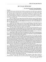
Figure 7 shows the change in reflectivity of a Ge–Sb thin
film with 15 at. % Ge, as a function of laser power and
duration measured by a static laser tester.62 The film was first
crystallized by annealing it in a furnace for 5 min at 300 ° C,
which is above this material’s crystallization temperature.62
A two pulse experiment was then performed. The first pulse,
of fixed time and power ͑100 ns for 50 mW͒, created a small
region of melt-quenched amorphous material at a previously
.c
om
Burr et al.: Phase change memory technology
co
233
FIG. 7. ͑Color online͒ ͑a͒ Relative change in reflectivity ⌬R / R in percent of
a crystalline Ge–Sb thin film with 15 at. % Ge as a function of laser power
and duration. The film was first crystallized by heating it in a furnace for 5
min at 300 ° C. A first pulse of fixed time and power ͑100 ns, 50 mW͒ was
applied to create melt-quenched spots in the crystalline film, and then a
second laser spot of variable power and duration at the same location was
used to recrystallize the amorphous spots. ͑b͒ Normalized change in reflectivity ͑in percent͒ integrated over a power range between 24 and 25 mW
from ͑a͒ as a function of laser pulse length. The dots are experimental data,
the line is a fit to 1 − exp− ͑t / ͒a, with t being the time, = 7 ns, and a = 3.
͑c͒ Relative change in reflectivity ⌬R / R in percent of an amorphous Ge–Sb
thin film with 15 at. % Ge as a function of laser power and duration. Note
that much longer pulses are required. Reprinted with permission from D.
Krebs et al., J. Appl. Phys., 106, 054308, 2009. © 2009, American Institute
of Physics.
unused spot in the crystalline film. Then a second laser spot
of variable power and duration, applied a few seconds later
at the same location, was used to recrystallize the amorphous
spot. Figure 7͑b͒ plots the normalized change in reflectivity
caused by this second pulse. Since the crystalline phase has a
higher reflectivity than the amorphous, the increase in reflectivity observed for all pulses longer than 5–10 ns, independent of applied power, indicates extremely fast recrystalliza-
JVST B - Microelectronics and Nanometer Structures
Redistribution subject to AVS license or copyright; see Download to IP: 86.31.48.42 On: Mon, 17 Mar 2014 09:16:29
CuuDuongThanCong.com
/>
Burr et al.: Phase change memory technology
234
cu
u
du
o
ng
th
.c
om
an
tion. Because this material is crystallizing the amorphous
spot predominantly by growth from the surrounding
crystalline-amorphous border, this time scales with the size
of the melt-quenched amorphous spot.97 In contrast, Fig. 7͑c͒
shows the much slower initial crystallization from the
amorphous-as-deposited phase of Ge–Sb measured in a
single-pulse experiment.35
Several factors contribute to nucleation and growth kinetics: temperature,98 composition,77,99,100 material interfaces,101
device
geometry,77,102
device
size,33,103
material
42,66
104
polarity,
and device history.96,97 Of these,
thickness,
the two most important factors governing switching speeds
are temperature and local composition. In fact, most of the
macroscopically observable nucleation effects associated
with geometry, size, thickness, device history, polarity, and
even material interfaces can be understood in terms of
the effects of varying local composition on the delicate
balance between surface and volume energies that drive
crystallization.
For any given composition, the crystallization properties
of a phase change material tend to be a strong function of
temperature. As shown in Fig. 8, the crystal growth speed
can vary by more than 15 orders of magnitude between room
temperature ͑which is off scale in Fig. 8͒ and the melting
point. The symbols in Fig. 8 correspond to growth speeds of
less than 10 nm/s, measured by exhaustive atomic force microscopy ͑AFM͒ at temperatures below 180 ° C.93 ͑These
data were taken for AIST, a growth-dominated material similar to GeSb, although both Ge2Sb2Te5 and Ge4Sb1Te5 were
measured to have very similar low-temperature growth
velocities93͒. The solid curve in Fig. 8 represents a simulation model built to match both these low-temperature experimental data as well as extensive recrystallization data for
GeSb measured on a static laser tester. These experimental
data included both reflectivity measurements similar to Fig. 7
ng
FIG. 8. ͑Color online͒ Crystal growth velocity ͑solid line͒ for GeSb as inferred by matching between simulation and empirical measurements. Low
temperature crystal growth speed was measured by monitoring the slow
growth of crystalline nuclei for growth-dominated ͑AIST͒ material ͑Ref.
93͒; high-temperature crystal growth speeds represent the best match between the measured optically induced recrystallization of amorphous marks
on thin film GeSb and simulations of this process ͑Refs. 93 and 105͒.
as well as AFM measurements of the size of melt-quenched
spots before and after laser pulses.105 The sharp increase in
crystal growth speed above the glass transition temperature
at 205 ° C is associated with a sharp drop in viscosity at
these temperatures, characteristic of “fragile glass-forming”
materials.106,107
This wide range of crystal growth speeds between moderate and high temperatures is one of the most important
features of phase change materials. It allows the amorphous
phase to remain unchanged for several years at temperatures
near room temperature, while at programming temperatures
crystallization can proceed in Ͻ100 ns. The kinetic response
of phase change materials to temperature has been described
by nucleation theory in great detail.107–109 Perhaps the most
influential parameters from nucleation theory involve the relation between the interfacial energy ͑energetic cost of adding material to a crystalline-amorphous interface͒ and the
free energy of crystallization ͑thermodynamic driving force
for crystallization͒. This interplay controls the size of the
critical or smallest stable nucleus, which in turn influences
the nucleation rate at which such nuclei can be incubated at
lower temperatures ͑typically reaching a maximum rate near
the glass transition temperature͒, and the growth rate at
which large nuclei expand into the surrounding undercooled
liquid ͑typically peaking at higher temperatures closer to the
melting point͒. The presence of these subcritical nuclei can
be detected by fluctuation transmission electron microscopy
͑FTEM͒,110 which can explore medium-range spatial correlations beyond the nearest atomic neighbor. Using FTEM, it
was observed that an increase in the population of subcritical
nuclei led to a decrease in the incubation time before
crystallization,110 as predicted by classical nucleation
theory.107
As discussed earlier, scaling is beneficial for PCM device
speed. For example, it was observed that the set time ͑crystallization time͒ and reset times ͑melt quenching͒ were reduced for Ge2Sb2Te5 material when device dimensions were
reduced from 90/1.5 ns for set/reset operation for 470 nm
diameter “pore” cell devices to 2.5/0.4 ns for 19 nm diameter
devices.33 Such results help move toward one important goal
of phase change materials research: The quest for materials
that can reliably switch at speeds comparable to RAM ͑approximately 10–50 ns͒ without sacrificing retention, endurance, or any other critical performance specification. Due to
the large number of experimental variables that can contribute to switching kinetics ͑thermal environment, deposition
conditions, changes, or damage induced during processing͒,
extrapolating from simple thin film recrystallization experiments to PCM devices remains difficult. Crystallization from
electrical pulses has been reported to range from 2.5 ns ͑Ref.
111͒ to 1 s ͑Ref. 112͒ for similar materials Ge2Sb2Te2 and
Ge2Sb2Te5, respectively.
There are certainly phase change materials that crystallize
at much higher speed than the widely used Ge2Sb2Te5 alloy.
For example, GeSb and Sb2Te3 are two high speed materials
that have been demonstrated to crystallize in tenths of nanoseconds, comparable to the performance of consumer
co
234
J. Vac. Sci. Technol. B, Vol. 28, No. 2, Mar/Apr 2010
Redistribution subject to AVS license or copyright; see Download to IP: 86.31.48.42 On: Mon, 17 Mar 2014 09:16:29
CuuDuongThanCong.com
/>
Burr et al.: Phase change memory technology
235
dT
= ٌ · ͑ ٌ T͒ + ͉J͉,
dt
and Laplace’s equation,
ٌ · ͑ ٌ V͒ = 0.
du
o
dC p
ng
th
an
Because of the large number of factors influencing the
performance of PCM devices, a number of groups have begun to perform predictive numerical simulations. Particularly
for the consideration of reducing the reset current that can
limit density by requiring a overly large access device, even
straightforward electrothermal modeling of the temperature
produced by a particular injected current can be highly revealing. Such electrothermal studies typically need to simultaneously solve the heat diffusion equation,
.c
om
C. Modeling of PCM physics and devices
ment techniques can include these effects and work well for
cylindrically symmetric cell designs, such as the conventional “mushroom” cell, since such structures can be reduced
to a single ͑r , z͒ plane. However, because of the inherent
computational difficulty in inverting matrices as they grow
very large, these techniques are difficult to extend to threedimensional cell designs. Finally, even though nucleation is
unlikely to play an effect during the fast reset pulse, recrystallization at the end of a reset pulse does play an important
role in the value of the reset current, especially for the
fastest-crystallizing phase change materials that hold the
most attraction for applications. The best case scenario
would be to have a finite-difference simulation tool capable
of handling large and arbitrary 3D structures, which could
potentially be matched against fast electrical set and reset
experiments, slow thin film crystallization experiments, and
optical pulse experiments performed with the same material.
From our experience with such a simulation tool,42 the
reset condition is not dictated by the maximum temperature
at the cell center, but by what happens at the edge of the cell.
Typically, a voltage pulse just below the reset condition
leaves a small portion of the limiting cross-sectional aperture
remaining in the crystalline state, usually at the extreme
edges of the cell.42 In general, besides the obvious choice of
reducing the diameter of this limiting aperture, the best way
to reduce the reset current is to improve the efficiency with
which injected electrical power heats the cell. In the best
case scenario, this power would heat just the portion of the
cell needed to block all of the cross-sectional apertures and
produce a high-resistance state. However, in any practical
case, the surrounding material is also heated to some degree.
Optimization can be performed by ensuring that the heated
volume is minimized and by reducing the heat loss through
the thermally conductive electrodes as much as possible. Another popular way to decrease reset current is to increase the
overall resistance of the cell by increasing the series resistance of the contact electrode,133 although it is not clear how
much of this benefit may be due to associated changes in
thermal resistance.
As with any simulation, care must be taken to establish
the boundary conditions correctly, because the computer
memory available for simulation is inevitably finite. For instance, Dirichlet boundary conditions, which call for the
edge of the cell to be held at room temperature, are frequently used128 and are easy to program. However, in a
simulation where the hot central region of the PCM cell is
not very far from this boundary, then the effective heat transfer over this boundary can become unphysically large, skewing the results. In contrast, Neumann boundary conditions, in
which the spatial derivative of temperature ͑or equivalently,
outgoing heat flow͒ is held constant at the boundaries, allow
a truncated simulation to act as if it is embedded within a
large expanse of surrounding material.
Another important consideration is the optimization metric. It is conventional in the PCM community to discuss the
importance of reset current. However, it is the dissipated
power, not current, which leads to the heating of the cell. The
ng
SRAMs. Phase change memory devices fabricated from
Ge–Te were shown to switch in resistance by nearly three
orders of magnitude with set pulses of 1 ns.36 Femtosecond
laser pulses have been demonstrated to induce disorder-toorder transition in amorphous GeSb films,42,113,114 indicating
very high speed potential. However, pulse duration is often
confused with material switching speed. This is an oversimplification: Crystallization and growth are thermally activated processes115,116 and removal of stimulation is followed
by a cooling period where additional crystal growth can contribute to observed phenomenon. Nevertheless, from a large
aggregate of reports we can expect first generation devices to
attain switching speeds of 20–200 ns. These phase change
materials have the significant advantage of being highly nonvolatile at temperatures near room temperature, while retaining fast-switching speeds at high temperature. Extensive materials and device research continues to decrease
crystallization times below these values,117,118 offering hope
of a bright future for PCM technology in application niches
that call for rapid switching.
co
235
͑2͒
͑3͒
cu
u
In these equations, temperature T and voltage V are each
computed as a function of time t. Even inside each material
of density d, parameters such as specific heat ͑C p͒, thermal
conductivity ͑͒, and electrical resistivity and conductivity
͑ and ͒ are frequently functions of both position and temperature. The current density J and the temperature dependence of the electrical conductivity serve to intimately cross
couple these two equations.
A number of studies have used analytical
equations,49,108,119–122 finite-element techniques,123–131 and
finite-difference techniques42,132 to analyze either PCM cells
or phase change material. Pirovano et al.41 studied the reset
current and the thermal proximity effect of scaled PCM by
both simulation and experiment. Although analytical techniques are attractively simple and work well for explaining
the incubation of new crystalline nuclei108 or threshold
switching,49 it is difficult to include the effects of inhomogeneous temperature distributions and temperature-dependent
resistivity, which critically affect the reset current through
their effect on the dynamic resistance of the cell. Finite eleJVST B - Microelectronics and Nanometer Structures
Redistribution subject to AVS license or copyright; see Download to IP: 86.31.48.42 On: Mon, 17 Mar 2014 09:16:29
CuuDuongThanCong.com
/>
236
Burr et al.: Phase change memory technology
236
focus on current comes from the assumption that a colocated
access transistor will have a current-voltage characteristic
that saturates. If the applied current needs to be higher than
this saturation value, there is no way for that particular transistor to supply it. This in turn implies that density will need
to be sacrificed in order to provide this current. In actuality,
the transistor and PCM device will interact in a complex
manner, with the transistor supplying power to the PCM device as if it were a load resistor. The added complexity is that
the dynamic resistance of the PCM device itself will in turn
be a strong function of this supplied power.122 An overly
tight focus on reset current can end up optimizing into a
shallow minimum in reset current, which in fact is quite
disadvantageous in terms of reset power.128
Since so many interlocking parameters influence the performance of PCM devices, especially as they become ultrasmall, an important part of scalability studies is the fabrication and testing of prototype PCM devices. Because only a
modest number of such prototype devices are typically fabricated and tested in research environments, these types of
experiments cannot hope to predict the actual device reliability statistics ͑yield, endurance, and resistance distributions͒
that can be expected from full arrays. However, prototype
devices are an extremely important test for the scalability of
PCM—if you cannot get any ultrasmall devices to operate
correctly, then this is a bad sign for the future of the technology. Here we will report on the properties of one such
prototype device: the bridge cell.
The phase change bridge cell is a relative simple testing
vehicle for studying novel phase change materials,42 extending the line-device concept that had been introduced earlier77
to ultrasmall dimensions. In these studies, two 80 nm thick
TiN electrodes separated by a planarized dielectric layer
were typically used as the contacts, with a thin phase change
bridge fabricated to connect the two electrodes. Bridge devices have been fabricated from various materials including
undoped and doped Ge–Sb with 15 at. % Ge, Ge2Sb2Te5,
Ag- and In-doped Sb2Te, Ge–Te with 15 at. % Ge, and thin
Sb phase change materials.34,42,78
After fabrication of these TiN bottom electrodes using
KrF lithography and chemical mechanical polishing, a thin
layer of phase change material ͑down to 3 nm thick͒ was
deposited by sputter deposition and capped with a thin SiO2
layer to prevent oxidation. Electron-beam lithography was
used to define the phase change bridge itself. Bridge widths
͑set by the e-beam lithography͒ varied between 20 and 200
nm, and the length ͑determined by the spacing between the
underlying electrodes͒ ranged from 20 to 500 nm. Figure
9͑a͒ shows a scanning electron microscope image of the
phase change bridge and the TiN electrodes, while Fig. 9͑b͒
shows a cross-sectional transmission electron microscope
image of a Ge–Sb bridge that is only 3 nm thick. Negative
photoresist was used to define the bridge so that the resist did
not need to be removed after the fabrication process. Ar ion
milling was applied to transfer the exposed photoresist pat-
tern into the phase change material, and a 50 nm thick layer
of SiO2 was subsequently deposited for protection.
These devices could be cycled through more than 30 000
set-reset cycles and the stored data were shown to survive
temperature excursions up to 175 ° C.42 These ultrasmall
devices—down to devices with cross-sectional apertures as
small as 60 nm2—correspond to effective switching areas
that will not be encountered by mainstream device technology until the 22 nm node, which Flash is expected to reach in
2015.5 Thus these bridge-device demonstrations show that
PCM will remain not only functional but robust through at
least the 22 nm technology node.
Several device parameters were measured as a function of
device geometry. Current-voltage ͑I-V͒ curves revealed typical PCM behavior with threshold switching. By modifying
the fabrication procedure so that the phase change material
never experienced any temperatures over 120 ° C, bridges
that remained in the amorphous-as-deposited phase could be
produced.34,35 This allowed the precise measurement of
threshold switching as a function of device length in a wellknown geometry. Each material was found to have a unique
threshold field, measured by determining the threshold voltage as a function of device length. These fields were 8, 19,
39, 56, and 94 V / m for Ge–Sb with 15 at. % Ge, Ag- and
In-doped Sb2Te, Ge–Te with 15 at. % Ge, Ge2Sb2Te5, and
thin Sb phase change materials, respectively.34,35 No
leveling-off of the threshold voltage with length was observed, although the shortest bridge devices were 20 nm, as
opposed to the nanowire devices where amorphous plugs
shorter than 10 nm were studied ͑Sec. II A͒. Unfortunately,
line edge roughness in the TiN electrodes ͓see Fig. 9͑a͔͒ led
to shorts between the long TiN electrodes for separations
smaller than 20 nm. Figure 10 demonstrates the scaling behavior of bridge devices in terms of the reset current. Both
measured reset current ͑dots͒ and the predictions of numerical simulations ͑lines͒42 decrease linearly with the crosssectional area of the bridge device. This indicates a favorable
cu
u
du
o
ng
th
an
co
ng
.c
om
D. Scalability of prototype PCM devices
FIG. 9. ͑a͒ Scanning electron microscope image of a phase change bridge
and its TiN electrodes. ͑b͒ Cross-sectional transmission electron microscope
image of a 3 nm thick GeSb bridge. Reprinted with permission from Y. C.
Chen et al., Tech. Dig. - Int. Electron Devices Meet., 2006, S30P3. © 2006,
IEEE.
J. Vac. Sci. Technol. B, Vol. 28, No. 2, Mar/Apr 2010
Redistribution subject to AVS license or copyright; see Download to IP: 86.31.48.42 On: Mon, 17 Mar 2014 09:16:29
CuuDuongThanCong.com
/>
237
Burr et al.: Phase change memory technology
237
FIG. 10. ͑Color online͒ Reset current of doped-GeSb phase change bridge
devices vs cross-sectional area defined by the lithographic bridge width W
and the ultrathin film thickness H. Reprinted with permission from Y. C.
Chen et al., Tech. Dig. - Int. Electron Devices Meet., 2006, S30P3. © 2006,
IEEE.
III. DESIGN AND FABRICATION OF PCM
du
o
ng
th
In this section, we discuss issues relevant to the design of
PCM cells, such as cell structures and access circuitry, as
well as those related to fabrication, such as the effects of
variability and the deleterious effects of semiconductor processing on PCM materials and devices.
A. Cell structures
ng
.c
om
FIG. 11. ͑Color online͒ Back-of-the-envelope estimate for the expected pulse
width and associated current density as function of the pitch 2F of the active
volume of the phase change material. Also shown are the empirical current
densities for a phase change bridge device ͓300 A for a H = 10 nm, W
= 30 nm bridge ͑Ref. 42͒, with the equivalent pitch for lithographic definition estimated to be 2ͱ͑10ϫ 30͒ ϳ 35 nm pitch͔, and 160 A for a 7.5
ϫ 65 nm2 dash-type cell ͑plotted for an equivalent 45 nm pitch͒.
co
We address this issue again in Sec. IV B where we discuss
cell-to-cell thermal cross-talk.
However, this computation allows us to set a lower bound
for the required current density to achieve melting. We can
use the expected pulse duration from Eq. ͑4͒ to satisfy the
minimum condition that the supplied energy should be large
enough to raise the temperature of the critical volume above
the melting point,
an
scaling behavior because the required reset current determines the size of the access device which in turn determines
the effective density of the PCM array.
It was possible to repeatedly cycle bridge devices fabricated from fast-switching Ge–Sb material with set and reset
pulses of 10 ns,34,35 confirming the observations of fast crystallization for this material seen in optical testing ͑Fig. 7͒.
Very short switching times and reduced switching times with
reduced device dimensions have also been observed for ultrascaled pore devices by Wang et al.33
cu
u
Over the next few technology generations, the most serious consideration for PCM is the large current needed to
switch PCM cells. We can roughly estimate this required
current using “back-of-the-envelope” calculations. The operation of the PCM cell relies on Joule heating, so the cell
structure and operating conditions are dictated by the electrothermal diffusion equation shown earlier ͓Eq. ͑2͔͒.
We can assume that the critical volume undergoing phase
change within the cell in a closely packed memory array is
laid out at a pitch of 2F. This immediately imposes the restriction that, to first order, the applied electric pulse width
should be such that the thermal diffusion length should not
exceed the half-pitch distance, F, in order to avoid cross-talk
during programming. Thus
F Ͼ ͱ2D ,
͑4͒
where D is the diffusion constant defined as ͑ / dC p͒ and is
the time duration of the applied electric pulse. This approximation is only good to first order, however, because thermal
diffusion through a one-dimensional ͑1D͒ geometry is not
identical to a 1D slice of diffusion through a 3D geometry.
J2 Ͼ dC p
⌬T
,
͑5͒
where ⌬T is the difference between the melting point of the
phase change material and ambient temperature. Note that
the energy spent to heat neighboring material, as well as any
inhomogeneous heating of the center of the critical volume
beyond the melting point, is not included.
Figure 11 shows a plot of pulse duration and, more
importantly, the lower bound on current density required to
heat the minimum volume. Here typical material parameters
for phase change materials have been used. This analysis
thus suggests that we will need to supply a current density of
at least 106 A / cm2 ͑104 A / m2͒ to be able to melt the
critical volume within the cell for reset.
In contrast, the measurements and simulations shown in
Fig. 10 would seem to indicate that the current density required is actually much larger, possibly as high as 300 A
for a 300 nm2 aperture, or 108 A / cm2 ͑106 A / m2͒.
However, the large expense of metallic electrodes in close
proximity to these tiny prototype devices actually makes this
number more pessimistic than is warranted. Other demonstrations, such as the 160 A reset current shown for a 7.5
ϫ 65 nm2 dash-type cells,134 seem to suggest a number such
as JPCM ϳ 3 ϫ 107 A / cm2 = 3 ϫ 105 A / m2. Because the
JVST B - Microelectronics and Nanometer Structures
Redistribution subject to AVS license or copyright; see Download to IP: 86.31.48.42 On: Mon, 17 Mar 2014 09:16:29
CuuDuongThanCong.com
/>
Burr et al.: Phase change memory technology
238
tion transistors ͑BJTs͒ ͑Ref. 44͒ or diodes43 or novel devices such as surrounding-gate transistor136 or FinFETs;137
• locally increase the current density within the phase
change element and decrease the switching volume by creating sublithographic features in the current path through
the PCM element.
ng
.c
om
Both of these approaches have been pursued aggressively
to demonstrate the basic operation of PCM technology. In
this section, we will focus on the latter path: optimization of
the phase change element itself by creation of a sublithographic aperture.
A typical PCM cell is designed so that the only current
path through the device passes through a very small aperture.
As this aperture shrinks in size, the volume of phase change
material that must be melted ͑and quenched into the amorphous state͒ to completely block it is reduced. In turn, this
decreases the power ͑and thus the current͒ requirements. If
this current is low enough, then a minimum-size access device can provide enough power to switch the cell from the
set state to the reset state.
In order to fabricate a PCM cell that will work even with
these small currents, an innovative integration scheme is
needed which creates a highly sublithographic yet controllable feature size. Subtle variations in cell design may have a
large impact on critical device characteristics, including endurance, retention, set and reset resistance distributions, and
set speed. These considerations will be the subject of Sec.
III C. The cell design must be scalable as well as highly
manufacturable since scaling implies not only a shrink in
physical dimensions of the memory cell but also an increase
in the number of memory cells per chip. Lastly, to maximize
the number of bits per cell, a cell structure which allows
multibit functionality is highly desirable.60,138
Depending on how this sublithographic aperture is implemented, PCM cell structures tend to fall into one of two
general categories: those which control the cross section by
the size of one of the electrical contacts to the phase change
material ͓contact minimized, Fig. 12͑a͔͒41,139–144 and those
which minimize the size of the phase change material itself
at some point within the cell ͓volume minimized, also known
as confined, Fig. 12͑b͔͒.41–43,77,103,124,138,145–147 The typical
volume-minimized cell structures tend to be a bit more thermally efficient, offering the potential for lower reset current
requirements compared to the contact-minimized
structures.41
ng
th
an
estimated numbers plotted in Fig. 11 represent a lower
bound, we will instead use this higher empirical value in the
remainder of this discussion.
In a full memory array, an access device such as a diode
or transistor must be included at each memory cell to ensure
that the read and write currents on each bit line are interacting with one and only one memory device at a time. The
amount of current that this access device can supply must
comfortably exceed the required reset current of the worstcase PCM element. Unfortunately, the CMOS field effect
transistors ͑FETs͒ often considered for use as access devices
in a PCM memory array have limited current drive capability; most optimized devices can provide only about Iacc
ϳ 800– 1500 A / m, where this current capability scales
linearly with the effective gate width of the drive transistor.
One way to solve this problem is to simply make the access
device larger so that it can drive a larger current. However,
since this immediately sacrifices memory density which subsequently drives up the cost per megabyte, such a move
would be economic suicide for a prospective memory
technology.
Given a transistor of width F, the available transistor
drive-current, IaccF, must exceed the required current for reset, JPCMF2, where is an area factor between 0 and 1.
Although returning to the set state does involve exceeding
the threshold voltage, the amount of power ͑and current͒ in
the set pulse is typically 40%–80% that of the reset pulse.
Thus it is almost always the reset pulse that must be considered when determining if the access device will supply sufficient current, while the set pulse is typically the factor that
dictates the write speed of PCM technology. Inserting the
numbers above produces
co
238
IaccF Ͼ JPCMF2 ,
5 nm Ͼ F,
du
o
͑1.5 ϫ 103 A/m͒F Ͼ ͑3 ϫ 105 A/m2͒F2 ,
͑6͒
cu
u
which implies that transistor current scaling could only hope
to catch up with the reset current of lithographically defined
PCM devices at ultrasmall technology nodes. This is especially sobering given that PCM reset current, as shown in
Fig. 10, has been empirically observed to scale with CD at a
pace somewhere between F1.5 and F1.0, rather than as F2.
This analysis implies that minimal-width FETs cannot
supply the necessary current if the dimensions of the phase
change volume are determined lithographically. However,
use of a factor ϳ 0.1, corresponding to a sublithographic
CD for the phase change element of roughly F / 3, allows Eq.
͑6͒ to be satisfied for F ϳ 45 nm, precisely where industry
has been targeting first PCM products.135 At this node, the
required reset current of 61 A ͑not that far from the demonstrated reset current in Ref. 134͒ could be supplied by the
CMOS transistor capable of 67 A.
Thus there are two parallel routes to ensuring sufficient
reset current for PCM devices:
• Use access devices that have higher current drive capability, including either known devices such as bipolar junc-
1. Contact-minimized cell
The most common contact-minimized cell structure is the
mushroom cell, where a narrow cylindrical metal electrode
contacts a thin film of phase change material. Figure 13
shows TEM images of mushroom cells in the set state ͑a͒
and in the reset state ͑b͒. In the reset state, an amorphous
dome of the phase change material—resembling the cap of a
mushroom, thus the name—plugs the critical current path of
the memory cell, resulting in an overall high-resistance state
for the cell. The bottom electrode contact ͑BEC͒, typically
made of TiN, is the smallest element in this cell. It is com-
J. Vac. Sci. Technol. B, Vol. 28, No. 2, Mar/Apr 2010
Redistribution subject to AVS license or copyright; see Download to IP: 86.31.48.42 On: Mon, 17 Mar 2014 09:16:29
CuuDuongThanCong.com
/>
239
Burr et al.: Phase change memory technology
239
FIG. 14. ͑a͒ TEM cross section of a pillar cell with a FET access device. ͑b͒
Close-up TEM cross section of GST/TiN pillar. The simulated reset current
dependence of this device is shown in Fig. 18͑a͒. Reprinted with permission
from T. D. Happ et al., Tech. Dig. VLSI Symp., 2006, 120. © 2006, IEEE.
th
co
an
FIG. 12. ͑Color online͒ Phase change device archetypes: ͑a͒ A typical
contact-minimized cell, the mushroom cell, forces current to pass through a
small aperture formed by the intersection of one electrode and the phase
change material. ͑b͒ A typical volume-minimized cell, the pore cell, confines
the volume of the phase change material in order to create a small cross
section within the PCM device. Reprinted with permission from S. Raoux et
al., IBM J. Res. Dev., 52, 465, 2008. © 2008, IBM.
ng
.c
om
this is too slow to be used commercially. The thin film of the
phase change material ͑or a stack of different phase change
materials149 with varying alloy concentrations͒ can then be
deposited over the planarized feature using standard techniques such as physical vapor deposition ͑PVD͒ or chemical
vapor deposition ͑CVD͒. The top electrode contact ͑TEC͒ is
also deposited, usually without breaking vacuum. The simplicity of the phase change material portion of the process—
and the ability to define the CD before any novel materials
are introduced—represents two of the most attractive features of the mushroom cell.
The deposited films are then patterned into islands using
conventional lithography to form individual cells, and isolated and encapsulated using thermally insulating dielectric
materials such as Si3N4.143 A variety of materials engineering
techniques has been introduced to optimize the cell performance, especially the minimization of reset current. These
include increasing the resistivity of either the electrode
material150 or the phase change material,133 and decreasing
the thermal diffusive losses through both the top and bottom
electrode regions.130,151
Although cells with horizontal heater electrodes have
been demonstrated,152 the vast majority of contactminimized cells closely resemble the mushroom cell. One
popular variant is the ring-electrode mushroom cell, where
the heater electrode consists of a thin ring of metal surrounding a center dielectric core.153 The incentive here is to reduce
both reset current and variability by decreasing the effective
area, since compared to a normal heater the metal annulus
has a smaller area, which also scales only linearly with CD.
cu
u
du
o
ng
mon to see this critical dimension ͑CD͒ described as the
“heater,” although the cell works most efficiently when the
heat is mostly generated in the phase change material at the
top of this BEC.
The sublithographic BEC can either be formed by a
spacer process,148 resist trimming,60 or by the key-hole transfer process,103 followed by chemical mechanical polishing
͑CMP͒ for planarization. The processing of phase change
materials is discussed in more detail in Sec. III D. Prototype
devices can use e-beam patterning to define the heater but
2. Volume-minimized cell
FIG. 13. TEM cross sections of a mushroom cell PCM element in the ͑a͒ set
state and ͑b͒ reset state. In the set state, the phase change material is polycrystalline throughout. In the reset state, a “mushroom cap” of amorphous
phase change material restricts the current flow through the bottom electrode. From Breitwisch, Phase Change Materials: Science and Applications.
© 2009 by Springer.
Significant research efforts have been spent exploring a
variety of volume-minimized cell structures, owing to their
superior scaling characteristics. However, achieving such a
structure can be a challenge, requiring the development of
processing technologies that can successfully confine the
phase change material within a sublithographic feature. The
most obvious structure in this category is the pillar cell ͑Fig.
14͒, where a narrow cylinder of phase change material sits
between two electrodes.138 This cell is fabricated in a similar
fashion to the mushroom cell, with a thin film stack of the
phase change material and top electrode material deposited
JVST B - Microelectronics and Nanometer Structures
Redistribution subject to AVS license or copyright; see Download to IP: 86.31.48.42 On: Mon, 17 Mar 2014 09:16:29
CuuDuongThanCong.com
/>
240
Burr et al.: Phase change memory technology
240
sary to enable continued scaling of pore cell devices.155 As
with nearly all PCM cell designs, the dimensions and aspect
ratio of the phase change material region critically influence
the reset current.
3. Hybrid PCM cells
.c
om
ng
B. Access circuitry
In order to fully leverage the scalability of PCM and thus
achieve the very high densities needed for SCM, the most
ideal implementation of PCM would be a cross-point array
cu
u
du
o
ng
th
an
atop a bottom electrode, and then patterned. However, in the
pillar cell, the BEC is large, and it is the phase change material that must be successfully and reliably patterned into
sublithographic islands. This patterning can be performed in
various ways, including lithography followed by resist
trimming.138 In addition to the challenges in controlling the
size of the patterned islands, this cell structure also suffers
from the drawback that the reactive ion etch ͑RIE͒ of the
phase change material can form a thin layer of altered alloy
composition at the surface, strongly affecting the performance and yield of the cell.154 This is discussed in further
detail in Sec. III D.
A modified version of the pillar cell structure is the pore
cell,103 where a sublithographic hole formed in an insulating
material atop the BEC is filled with the phase change material ͑Fig. 15͒. Conformal filling of nanoscale holes with high
aspect ratio is difficult using conventional PVD processes;
hence development of CVD or atomic layer deposition
͑ALD͒ technology for phase change materials will be neces-
co
FIG. 15. TEM cross section of a 45 nm bottom CD low aspect-ratio pore cell
filled with a PVD GST process. The simulated reset current dependence of
this device is shown in Fig. 18͑b͒. Reprinted with permission from M.
Breitwisch et al., Tech. Dig. VLSI Symp., 2007, 100. © 2007, IEEE.
The most advanced scaling demonstration of PCM technology to date was realized using the volume-confined
bridge cell,42 which consists of a narrow line of ultrathin
phase change material bridging two underlying electrodes
͑Fig. 9͒. The cross-sectional area of this device is determined
by film thickness in one direction and by electron-beam lithography in the other, allowing the realization of functional
cells with cross-sectional area of about 60 nm2 and reset
current requirement of about 80 A.
The -trench cell139 and the dash-confined cell134 are examples of PCM cells that combine the contact-minimized
and volume-minimized approaches. The -trench cell is an
extension of the bridge concept, with a PCM element formed
at the intersection of an underlying sidewall-deposited CVD
TiN bottom electrode and a trench of phase change material
formed at right angles across this electrode ͑Fig. 16͒. The
dash-confined cell134 is an extension of the pore cell idea,
except that the bottom electrode contact is formed by a
spacer process. A CVD process is then employed to fill in the
rectangular sublithographic holes formed by the recess etch
into the metal BEC ͑Fig. 17͒. In all three of these cases, one
critical dimension associated with the limiting crosssectional aperture is controlled by a thin film deposition process. As a result, only one dimension inherits the variability
of the lithography process. Conversely, of course, only one
dimension will enjoy the associated scaling benefits as F
shrinks from one technology node to the next.
FIG. 16. Illustration of the -trench cell, showing two neighboring devices with a common top electrode ͑e.g., along the bit line͒. Current passes through an
aperture which is limited in one dimension by the thickness of the underlying sidewall-deposited metal heater, and in the other dimension by the width of the
narrow trench in which phase change material ͑here, GST͒ is deposited. Reprinted with permission from F. Pellizzer et al., Tech. Dig. VLSI Symp., 2004, 18.
© 2004, IEEE.
J. Vac. Sci. Technol. B, Vol. 28, No. 2, Mar/Apr 2010
Redistribution subject to AVS license or copyright; see Download to IP: 86.31.48.42 On: Mon, 17 Mar 2014 09:16:29
CuuDuongThanCong.com
/>
Burr et al.: Phase change memory technology
241
cu
u
du
o
ng
th
.c
om
an
architecture, where each memory element in the array is directly connected to two orthogonal lines ͑Fig. 5͒. In fact, a
novel architecture has been proposed for such a direct crosspoint memory, in which PCM devices are switched not between set and reset, but between the reset state and an overreset state ͑strongly reset state͒.156 Even though these
resistances may differ, the difference in read current would
be too low to support rapid read. However, because the
threshold voltage varies between these two states, the device
state can be sensed by detecting whether a “read” voltage
intermediate between these levels produces an electrical
switching event. While this scheme does cleverly avoid an
access device, it has several serious issues. The margins between the read and the two threshold voltages are uncomfortably tight, and it would be difficult to detect the breakdown
without potentially heating up the cell, which means that
reads must be treated as destructive. Even so, typical reset
resistances are still low enough that the leakage through
“half-selected” devices ͑those that share either the same bit
line or the same word line as the “selected” device͒ would be
quite high, thus limiting the maximum array size ͑and the
effective memory density͒ that could be built. Worst of all,
the strong negative correlation between switching energy and
endurance ͑which will be discussed in detail in Sec. IV C͒
means that improving the sense margin by increasing the
resistance ͑and thus the threshold voltage͒ of the over-reset
state will sharply reduce endurance.
Thus the integration of PCM into an array architecture
seems to require the use of an access device: either a
diode,43,157 a field effect transistor,158,159 or a bipolar junction
transistor.44,61 The main role of this device is to minimize the
leakage current that would otherwise arise from the nonselected cells in the array. As has been mentioned, the most
important unknown for the success of PCM technology is
whether this memory access device is able to provide sufficient current to reset the PCM cell. While a diode can provide a current-to-cell size advantage over a planar transistor
down to the 16 nm node,160 the diode scheme is more vulnerable to write disturbs due to bipolar turn-on of nearestneighbor cells.43 A 5.8F2 PCM diode cell has been demonstrated using a 90 nm technology, in which the diode was
ng
FIG. 17. TEM cross section of the dash-confined cell, showing devices fabricated by a spacer process that are only 7.5 nm wide, and 65 nm deep in the
orthogonal direction. Reprinted with permission from D. H. Im et al., Tech.
Dig. - Int. Electron Devices Meet., 2008, 9. © 2008, IEEE.
able to supply 1.8 mA at 1.8 V.43 In comparison, a 90 nm
10F2 trigate FET could only supply approximately half as
much current.43
Although the raw footprint of the access device is of primary concern for memory density, other considerations can
also come into play. Peripheral circuits, such as charge
pumps to increase the voltage supply level or special read
and write circuitry for MLC operation,161 reduce the portion
of the chip that can be dedicated to memory devices ͑the
array efficiency of the chip͒. In addition, the effective area
per cell can grow because of additional vias or wiring that
may be required within the memory array. For instance,
given the high currents required for PCM programming, the
voltage drop along metal bit and word lines can become
significant, further reducing the power that can be delivered
to the actual PCM cell. Thus splitting an array in half to
reduce the maximum line length is attractive because it reduces the worst-case line loss, but detrimental because chip
real estate is now being used for redundant wiring rather than
memory devices. Particularly problematic is the wiring that
must sit under the PCM layer ͑such as common-source lines,
as well as the word lines to transistor gates͒ since these lines
must typically use high-resistance tungsten or polysilicon.
Because of the significant voltage losses in such lines, a via
must often be introduced every few ͑e.g., four or eight͒ cells
in order to strap this line to an overlying low-resistance copper line. This extra via immediately increases the effective
footprint per memory cell. Although copper cannot be introduced near the transistors, lest the CMOS devices become
degraded, one solution would be to move the PCM devices
higher up away from the silicon so that a layer of copper
interconnect can be fabricated under the PCM devices.
co
241
C. Variability
Different types of variability can affect the operation, performance, endurance, and reliability of PCM devices, ranging from intercell variability introduced during processing,
intercell variability as resistances change over time after programming, and cycle-to-cycle variation of the set and reset
resistances of any given cell ͑intracell variability͒. While the
read voltage, the reset pulse, and the set pulse can be optimized for the average memory cell, variations between cells
must be minimized so that these same choices can successfully operate all the cells in the memory array. The same is
true for the performance of the access device.
Any fabrication- or process-induced variability in the
physical structure of the phase change element can result in
devices which react differently to the same stimuli. Thus any
large collection of phase change elements, which because of
variability are in similar yet nonidentical states, may then
propagate in time on different resistance trajectories. In addition to group behavior caused by intercell variability, there
is also intracell variability produced by motion and
rearrangement of the atoms within the active region of the
phase change device during the programming of the phase
change device. Understanding the variability of PCM devices is particularly important in the context of multibit stor-
JVST B - Microelectronics and Nanometer Structures
Redistribution subject to AVS license or copyright; see Download to IP: 86.31.48.42 On: Mon, 17 Mar 2014 09:16:29
CuuDuongThanCong.com
/>
242
Burr et al.: Phase change memory technology
242
age capability, due to the reduced margin between resistance
levels that must be correctly sensed in order to successfully
retrieve data. Finally, variability can be expected to play an
increasingly important role in the scaling of PCM technology
into future technology nodes.
ng
co
FIG. 18. ͑Color online͒ ͑a͒ Reset currents for the pillar cell and the mushroom cell both show a strong dependence on the critical aperture size. Reprinted with permission from T. D. Happ et al., Tech. Dig. VLSI Symp.,
2006, 120. © 2006, IEEE. ͑b͒ The pore cell reset current is both strongly
dependent on the aperture size and shape ͑pore slope͒. ͑Figure 10 shows
how the reset current of the bridge cell scales directly with the crosssectional area of the phase change material.͒ Reprinted with permission
from M. Breitwisch et al., Tech. Dig. VLSI Symp., 2007, 100. © 2007,
IEEE.
cu
u
du
o
ng
th
an
Each step in the process of fabricating a wafer of PCM
memory devices is typically associated with one or more
physical attributes ͑e.g., thickness, CD, sidewall angle, etc.͒,
each with a nominal target value. To illustrate the variability
challenge inherent in wafer-level fabrication process, features on the order of nanometers ͑10−9 m͒ must be accurately controlled across the surface of a wafer which spans
nearly a third of a meter ͑0.3 m͒. Exact control over such a
large range of dimensions is impossible. Consequently, each
process is associated with an acceptable range around some
target value.
Furthermore, this fabrication process must construct a
fully integrated set of devices comprising a CMOS technology ͑CMOS field effect transistors, diodes, resistors, capacitors, wiring levels, and the vias connecting them͒ in addition
to the PCM devices ͑which usually reside on top of the
CMOS devices, at the bottom of the wiring levels͒. Thus a
wafer will undergo hundreds of processing steps ͑including
photolithography, atomic implant, reactive ion etch, material
deposition, chemical mechanical planarization, wet etches,
etc.͒, each with associated variability, before the final processed wafer is ready for the dicing and packaging of the
chips. Variability in processes that affect either the structure
of the phase change element or the access device ͑transistor,
diode, etc.͒ can contribute to the overall phase change device
variability. These structural variations then translate into
variations in electrical ͑device operation͒ properties of the
device.
Most relevant to the operation of PCM are the structural
physical properties, which affect the temperature profile
͑how much heat is generated and where͒, the critical limiting
cross-sectional aperture ͑which must be fully blocked to get
high resistance contrast͒, and the volume where the phase
change material undergoes repeated melting and crystallization. Crucial features of the cell are the aperture size and
shape, the thickness and uniformity of the phase change material ͑in both stoichiometry and doping͒, the resistivity and
interface resistance of electrodes, the thermal conductivities
of surrounding materials, and the stresses on the active
switching volume introduced by surrounding material.
As discussed in Sec. III A, several cell structures have
been proposed and developed in order to minimize the required power ͑current͒ for reset. Each of these structures
employs a similar strategy for minimizing the reset power:
At one and only one point within the cell, the electrical current is forced to pass through a small aperture. This aperture
increases the current density, maximizing the thermal power
which is generated, and reducing the volume of high resistivity material needed to significantly alter the external device resistance. Together with the electrical and thermal
.c
om
1. Structural variability
properties of the phase change material, electrodes, and surrounding materials, the size and shape of this aperture determines the temperature profile obtained within the phase
change element for a given set or reset programming current
pulse.
In order to estimate the impact of small variations of the
aperture size on the cell operation, it is instructive to examine the functional dependence of the aperture size on the
required reset programming current. We show the published
dependence of the reset current on the aperture size for the
bridge cell ͑Fig. 10͒, the pillar and mushroom cells ͓Fig.
18͑a͔͒, and the pore cell ͓Fig. 18͑b͔͒. In each case, the required current is a steep function of critical dimension. Variability introduces a distribution of PCM cells of different
sizes and thus different reset currents. In order to be sure to
be able to reset all of the devices, it is thus the largest diameter cell that dictates the required current-driving capability
of the access device. Variability directly reduces density by
mandating a larger-area access device. At the same time, as
we will see in Sec. IV C, switching cells with more power
than is necessary has a strong and negative influence on device endurance. Thus this same variability may also reduce
endurance in the smaller-area devices, which are being
driven much harder than they really need to be.
J. Vac. Sci. Technol. B, Vol. 28, No. 2, Mar/Apr 2010
Redistribution subject to AVS license or copyright; see Download to IP: 86.31.48.42 On: Mon, 17 Mar 2014 09:16:29
CuuDuongThanCong.com
/>
Burr et al.: Phase change memory technology
243
FIG. 19. ͑a͒ Collar process is used to create a sublithographically sized TiN
bottom electrode. First, a lithographically defined hole of diameter D is
etched into a SiON/SiN stack. A first collar is formed by depositing a conformal SiON layer followed by a collar RIE step. A second collar is formed
in the same manner. Next, the CVD TiN is deposited to fill the hole. Finally,
a series of CMP and oxide etch back processes are performed, resulting in a
cylindrical TiN bottom electrode. ͑b͒ A TiN ring electrode is constructed in
a similar manner except that only a thin layer of CVD TiN is deposited into
the hole, and then the center of the hole is filled with oxide. Original figure
from Ref. 140. From Breitwisch, Phase Change Materials: Science and Applications. © 2009 by Springer.
FIG. 20. ͑a͒ Sublithographic and lithography-independent feature is fabricated using the keyhole-transfer process: ͑1͒ A lithographically defined hole
is etched and ͑2͒ the middle SiO2 layer is recessed. ͑3͒ A highly conformal
poly-Si film is deposited, producing a sublithographic keyhole whose diameter is equal to the recess of the SiO2 layer. ͑4͒ The keyhole is transferred
into the underlying SiN layer to define a pore, followed by ͑5͒ removal of
the SiO2 and poly-Si. ͑6͒ The phase change and top electrode ͑TiN͒ materials are then deposited and the cell is patterned for isolation. ͑b͒ A SEM
cross section corresponding to step ͑3͒, showing keyholes for two different
sized lithographically defined holes. Since the keyhole size does not depend
on lithography, the phase change CD can be successfully decoupled from
any lithographic variability. From Breitwisch, Phase Change Materials: Science and Applications. © 2009 by Springer.
.c
om
243
co
dercut into the sidewalls of the hole, despite poor control
over the actual lithographically defined diameter of the hole
itself. Figure 20 describes this process and shows how the
keyhole process can produce identical sublithographic holes
͑30 nm͒ despite significant variation in the much larger lithographically defined holes ͑243 and 302 nm͒.
The keyhole-transfer process has been experimentally
demonstrated to decouple the final aperture size from the
initial lithographically defined hole size.103 Over a span of
initial lithographically defined hole sizes, the distribution of
reset current was found to be consistently narrower for pore
cells fabricated through the keyhole-transfer method than for
those fabricated with a collar process. Similar results have
been demonstrated for mushroom cells.122 Here, mushroom
cells with heaters defined with the keyhole-transfer process
were compared to otherwise identical mushroom cells with
heaters defined by trimming of photoresist islands. This comparison was performed by examining the dynamic resistance
Rdyn during programming, which tends to exhibit a dependence on programming current I as
cu
u
du
o
ng
th
an
There are several ways a sublithographically sized aperture can be defined. Not surprisingly, the degree to which the
aperture size can be controlled varies for each of these
methods.162 A direct way to reduce the size of a lithographically defined hole is to implement a collar process, as shown
in Fig. 19. Similarly, a subtractive method can be used ͑as in
the pillar cell scheme138͒, where an island of lithographically
patterned photoresist is trimmed in size using RIE and then
used as a mask to transfer the sublithographic pattern down
into the underlying layers. Unfortunately, in both of these
techniques, any variability in the diameter of the original
hole ͑or photoresist pillar͒ introduced by either lithography
or etch ͑or resist development͒ transfers directly to the final
CD. Thus the fractional variability ͑⌬CD/ CD͒ can become
uncomfortably large.
The -trench cell,139 the ring bottom electrode mushroom
cell,153 the dash-confined cell,134 and the bridge cell42 define
one of the dimensions of the cross-sectional area of the aperture through film deposition. The thickness of such deposited film can be tightly controlled, especially for CVD and
even more so for ALD techniques. This thickness can easily
be much thinner than the lithographic dimension F ͑at least
for current and near-future technology nodes͒. This method
of defining one dimension of the aperture by film thickness is
inherently decoupled from any lithographic variability. However, for these schemes, lithography is still needed to define
the “other” dimension of the aperture.
A keyhole-transfer process has been developed for PCM
devices, which decouples both dimensions of the final aperture from lithography. Here, a keyhole is defined within a
lithographically defined hole by film deposition. Typically, a
keyhole is undesired and indicates a failure to fill the hole.
However, the advantage is that the dimension of the keyhole
itself can be tightly controlled by accurate control over the
hole depth ͑through film deposition͒ and over the etched un-
ng
2. Sources of structural variability
Rdyn =
A
+ B.
I
͑7͒
Here the term A depends only on material characteristics,
while B incorporates both material and structure-dependent
factors.122 Thus the lower variability in B empirically observed for mushroom cells with heaters defined by the
keyhole-transfer method ͑as compared to those defined by
trimmed photoresist͒ is indicative of the tighter CD control
offered by the keyhole-transfer method.
3. Impact of structural variability
Structural variability gives rise to variability in electrical
response, which leads to broader resistance distributions after
single-shot programming. Figure 21 shows a series of set
JVST B - Microelectronics and Nanometer Structures
Redistribution subject to AVS license or copyright; see Download to IP: 86.31.48.42 On: Mon, 17 Mar 2014 09:16:29
CuuDuongThanCong.com
/>
Burr et al.: Phase change memory technology
244
cu
u
du
o
ng
th
.c
om
an
resistance distributions, including one ͑for 100 ns set pulses͒
which is strikingly broad. Although the majority of cells can
reach a low resistance of approximately 2 k⍀ with a set
pulse of 100 ns duration, for this collection of cells there is a
subset of devices whose resistances after such a single set
pulse extend all the way out to the fully reset resistance of
several hundred kilo-ohms. For a given programming current
amplitude, devices with different diameters will present different dynamic resistances during programming, thus dissipating different amounts of power despite the same drive
voltages. This variable power will lead to a different maximum temperature, and even a different temperature distribution within the cell because variations in aperture or heater
size affect the thermal resistances within the cell. For reset
pulses, the size of the amorphous plug required to significantly affect the room temperature low-field resistance of the
cell changes drastically with changes in the cross-sectional
aperture of the cell. In terms of set pulses shown in Fig. 21,
rapid set requires that the optimal temperatures for crystal
growth be present at the crystalline-amorphous boundary
͑growth-dominated material͒ or within the cell interior
͑nucleation-dominated material͒. Since the crystallization
speed is a strong function of temperature ͑Fig. 8͒, variability
in aperture size can result in a variety of incompletely set
cells if the pulse is too short. As Fig. 21 shows, increasing
the duration of set pulses tends to overcome this effect. Another even more effective route is to ramp down the set pulse
slowly, allowing each cell to pass through the temperature
for maximum crystal growth.163
In addition to broadened resistance distributions, device
variability also affects how these resistances evolve over
time. It is well known that the resistance of cells in the reset
state tends to increase slowly over time, an effect which has
been attributed to either mechanical relaxation forced by the
reduced density associated with the amorphous state,164,165 to
the formation of electronic traps associated with lone-pair
states which increases resistance by repositioning the Fermi
level,91 the annihilation of defects by trap filling which reduces transport and thus increases resistance,89,166 or to some
combination of these effects. Since this drift increases the
already high resistance of the reset state, it is not an issue for
binary PCM devices. However, drift can be particularly
problematic in the context of multiple bits per cell, as discussed in Sec. V A.
Drift would be bad enough if all cells changed in resistance along the same trajectory. However, variability introduces different drift coefficients, so that cells with similar
resistances immediately after programming tend to separate
in resistance over time. In addition, some variability in crystallization speed has been observed over large arrays of PCM
devices, so that some cells tend to set more easily ͑both at
elevated temperature and after low-temperature anneals͒ than
the average cell.167 Figure 22 illustrates the signature of this
effect, with reset tail bits emerging when a reset programming pulse with an insufficiently short quench time is used
for programming. Although such anomalous devices can be
reset to high resistance by using pulses with rapid quench,
such tail-bit devices will still be associated with increased
long-term retention loss and resistance distributions that
broaden more rapidly over time. In general, combining the
effects of drift and recrystallization, variable drift effects
tend to broaden the resistance distribution of a large collection of cells over time: Some cells increase in resistance due
to structural relaxation, some cells decrease due to partial
recrystallization. While some may first increase and then
only later decrease, the random walk nature of these effects
typically leads to broader distributions over time.
ng
FIG. 21. Set resistance and reset resistance distributions as a function of the
programming pulse width. In this example, while 100 ns is sufficient to set
most of the cells to below 2 k⍀, many cells still have a resistance greater
than 10 k⍀. However, extending the 50 ns reset pulse to 100 ns has no
noticeable effect on increasing the resistance of the reset tail. GST refers to
the phase change material used in this experiment, Ge2Sb2Te5 ͑Ref. 249͒.
Reprinted with permission from S. Kang et al., IEEE J. Solid-State Circuits,
42, 210, 2007. © 2007, IEEE.
FIG. 22. ͑Color online͒ Reset tail modulation by the quenching time tQ. A
long quench time results in a partial set of a small fraction of devices within
a large array. Reprinted from with permission from D. Mantegazza et al.,
Solid-State Electron., 52, 584, 2008. © 2008, Elsevier.
co
244
4. Intradevice variability
The act of programming a PCM cell involves the rearrangement and movement of atoms within the cell. When a
given cell, starting from the polycrystalline set state, is melt
quenched and then crystallized back to the set state, the distribution of crystal grains within the cell is not identical. The
J. Vac. Sci. Technol. B, Vol. 28, No. 2, Mar/Apr 2010
Redistribution subject to AVS license or copyright; see Download to IP: 86.31.48.42 On: Mon, 17 Mar 2014 09:16:29
CuuDuongThanCong.com
/>
Burr et al.: Phase change memory technology
245
.c
om
butions using iterative write attempts, where the length of the
trailing edge of the pulse is carefully controlled based on the
just-accumulated prior experience with that cell. Such iterative write schemes and other considerations of multilevel cell
programming are discussed in more detail in Sec. V A.
6. PCM scaling and variability
As PCM devices scale into future technology nodes, variability can be expected to become an even more important
consideration. Difficulties in scaling lithography and processing techniques may lead to even looser specifications on
relative CD uniformity in future technology nodes since the
acceptable range of control will be driven by considerations
for conventional CMOS devices and not by PCM technology. At future technology nodes, PCM cell designs which
depend on control over film thickness may no longer be as
attractive, if CD is shrinking while both the minimum thickness t and the achievable control of this variable, ⌬t, remain
relatively static. As the number of atoms participating in the
cu
5. Variability and MLC
u
du
o
ng
th
an
nucleation of these crystalline grains within the amorphous
plug leads to a decrease in reset resistance, which accelerates
at elevated temperature.168,169 It has been shown that a small
fraction of cells in the reset state will tend to show these
effects more rapidly than the average cell, but that the location of these cells is random from cycle to cycle. A cell may
participate in this tail of the resistance distribution on one
cycle, yet show much improved resistance to the anneal upon
the next, consistent with random nucleation of crystalline
grains within the amorphous plug.169 Thus we can expect
that this random formation of crystalline grains is present
throughout the portion of the cell that reaches elevated
temperatures.
Upon the application of a subsequent programming pulse,
the temperature distribution of the cell may not be exactly
identical to the previous cycle, leading to variations in resistance. This intradevice programming variability can be
readily observed in any single-cell endurance plot, as illustrated in Fig. 23.
ng
FIG. 23. Cycling performance of the set and reset states of a single PCM
cell. Reprinted with permission from S. Lai and T. Lowrey, Tech. Dig. - Int.
Electron Devices Meet., 2001, 3651. © 2001, IEEE.
FIG. 24. ͑Color online͒ Resistance distribution of a four-level cell using
single-pulse programming. Process-induced variations cause distributions to
overlap because the same applied voltage pulse leads to different temperatures in different cells. Reprinted with permission from T. Nirschl et al.,
Tech. Dig. - Int. Electron Devices Meet., 2007, 17.5. © 2007, IEEE.
co
245
Variability also forces the use of iterative write schemes
for programming of multilevel resistance states, as illustrated
in Fig. 24.60 Here, a collection of cells is programmed with
single current pulses, with the trailing edges controlled to
produce intermediate resistance values. The highest and lowest resistance levels have the smallest variation in
resistance—for these states the reset and set resistances tend
to saturate, as overly large voltages produce little additional
increase in reset resistance and overly long pulses produce
little additional decrease in set resistance. The intermediate
resistance levels, which represent hybrid states where a
smaller portion of the cell is amorphous than in the full reset
state,170 are much more sensitive to variability.
Even so, since each given cell does respond in a somewhat reproducible and hence predictable manner, the desired
resistance value can be produced by an iterative write
scheme. As illustrated in Fig. 25, the same cells used in Fig.
24 can be programmed into relatively tight resistance distri-
FIG. 25. ͑Color online͒ 10ϫ 10 array ͑100 devices͒ test structure programmed into 16 levels. Tight, well-controlled distributions allow 4 bits/
cell. Iterative adjustment of pulse slopes depending on the programmed
resistances is one method for achieving narrow distributions. Reprinted with
permission from T. Nirschl et al., Tech. Dig. - Int. Electron Devices Meet.,
2007, 17.5. © 2007, IEEE.
JVST B - Microelectronics and Nanometer Structures
Redistribution subject to AVS license or copyright; see Download to IP: 86.31.48.42 On: Mon, 17 Mar 2014 09:16:29
CuuDuongThanCong.com
/>
Burr et al.: Phase change memory technology
246
2. Etching
Etching of phase change materials has been explored using both wet as well as dry etching schemes. Such steps are
important for electrical isolation in most cell designs, and are
absolutely critical for cell designs such as the pillar cell that
depend on subtractive processing to produce a confined volume of phase change material. Some important parameters
that are studied in developing etch processes are etch rate,
selectivity ͑i.e., how fast the desired PCM etches compared
to the masking layer and other surrounding films͒, and anisotropy ͑etched sidewall angle; steeper profiles are usually
desirable since they enable higher resolution patterning͒. It is
also important to understand etch-induced material modification and other sidewall damage effects since these could impact device operation, especially if the damaged portion is
close to or part of the active switching volume of the PCM.
A number of groups reported wet etching of phase change
materials using alkaline175–177 as well as acidic178,179 solutions. Depending on the etchant and specific phase change
material etched, in some cases the crystalline material was
found to have etched faster than the amorphous phase while
the opposite was true in other cases. Cheng et al.178 used
x-ray photoelectron spectroscopy ͑XPS͒ and inductively
coupled plasma ͑ICP͒ to study the wet etch mechanism of
GST. They explained their results, obtained with a 20%
aqueous solution of nitric acid, as a chemical etching process
that involves bond breakage, oxidation of the various constituents, and dissolution of those oxides. They inferred that
the Sb component was hardest to etch. The authors used this
wet etching process to fabricate large PCM cells ͑400
ϫ 400 m2͒ and performed I-V measurements showing successful switching of devices from the high- to low-resistance
states.
an
Most studies related to the integration and processing of
PCM technology focus on the popular variant, Ge2Sb2Te5,
here abbreviated simply as GST, along with various choices
of dopant. This reflects the fact that GST possesses many
favorable characteristics and has thus received the bulk of
attention of technologists attempting to take PCM technology from research to development. Although these studies
reveal numerous characteristics which might be considered
less than perfect, the mere existence of such a large base of
knowledge also represents a substantial hurdle for any alternative phase change material hoping to challenge GST.
.c
om
D. Processing
measurements showed that the GST had a hexagonal phase
and was thermally stable up to 400 ° C. CMP was used to
planarize the GST, confining it to the contact holes ͑and removing it from everywhere else͒. Devices fabricated with
this technique showed a significant reduction in reset current
as well as good endurance. Im et al.134 used CVD GST to fill
high aspect-ratio ͑4:1͒ dash-type contacts of 7.5 nm width.
As expected from device modeling, these cells showed very
low ͑160 A͒ reset currents. In addition, these devices also
had fast set speeds and very good endurance.
Lee et al.174 developed ALD of GST with the assistance
of a H2 plasma. They synthesized new precursors for the
GST deposition and obtained good step coverage ͑90%͒ in
7:1 aspect-ratio holes. Finally, Milliron et al.71 developed a
solution-based deposition method for GeSbSe films using
hydrazine and Se to form soluble precursors, so that film
composition and properties were tunable through appropriate
combination of these novel precursors in solution. XRD and
laser pulse annealing were used to study the phase change
and crystallization speed, and complete filling was demonstrated in 2:1 aspect-ratio vias patterned in thermal silicon
oxide.
ng
active portion of the PCM cell decreases, any variations in
local doping or stoichiometry can be expected to affect individual cells, reducing yield and further broadening distributions. Eventually, in the same way that Poissonian effects
have arrived for CMOS devices ͑e.g., as the number of dopants in the channel becomes countable͒,171 such few-atom
effects can be expected to be observable for PCM. That said,
all logic and memory devices seeking to operate in this regime will have some variant of these effects—the winners
will be those with not-yet-known physics that keeps those
effects sufficiently unlikely, or those amenable to not-yetinvented engineering techniques that can finesse these issues
to an acceptable degree.
co
246
1. Deposition
cu
u
du
o
ng
th
The vast majority of phase change materials reported in
literature have been deposited by sputtering, i.e., PVD. Sputter deposition from multiple targets makes it very simple to
try different compositions. However, sputtered films typically do not have good step coverage and cannot completely
fill high aspect-ratio vias without keyhole formation.103 A
number of interesting PCM cell structures have been discussed ͑Sec. III A͒ that call for confining the phase change
volume inside a contact hole ͑or “pore”͒ formed in a dielectric, primarily to reduce the reset current. It is therefore essential to examine alternatives to sputter deposition for GST
and other phase change materials that can successfully fill
higher aspect-ratio vias.
Cho et al.146 developed a novel GST sputter deposition
process with in situ deposition/etch/deposition, in order to fill
GST into high aspect-ratio ͑Ͼ2 : 1͒ pores of approximately
50 nm diameter. A number of groups134,155,172,173 have investigated CVD of GST and related phase change materials.
Kim et al.172 deposited hexagonal phase GST by metal oxide
chemical vapor deposition at temperatures in the range of
330– 370 ° C using precursors that were bubbled at different
temperatures, demonstrating complete filling into 120 nm diameter trenches with aspect-ratio larger than 1.6. However, it
should be noted that in contrast to sputter deposition, CVD
processes are far less flexible with respect to changes in material composition.
Lee et al.155 used CVD to deposit GST from metalorganic precursors and hydrogen at 350 ° C into high aspectratio ͑3:1͒ 50 nm contact holes. X-ray diffraction ͑XRD͒
J. Vac. Sci. Technol. B, Vol. 28, No. 2, Mar/Apr 2010
Redistribution subject to AVS license or copyright; see Download to IP: 86.31.48.42 On: Mon, 17 Mar 2014 09:16:29
CuuDuongThanCong.com
/>