Studying the structure and some properties of R.F. Magnettron sputtered ZnO: al films
Bạn đang xem bản rút gọn của tài liệu. Xem và tải ngay bản đầy đủ của tài liệu tại đây (967.75 KB, 4 trang )
<span class='text_page_counter'>(1)</span><div class='page_container' data-page=1>
VNU. JOURNAL OF SCIENCE. Mathematics - Physics, T.xx, N03AP. 2004
<b>STUDYING THE STRUCTURE AND SOME PROPERTIES </b>
<b>OF R.F. MAGNETRON SPUTTERED ZnO: A1 FILMS</b>
<b>N go T hu H uon g, T a D in h C an h, N gu y en D u y P h u o n g , N g u y e n N g o c L ong</b>
<i>D epartm ent o f Physics, College o f Science, V N U</i>
Abstract: structural, optical and electrical properties of Al-doped ZnO films,
deposited by r.f. magnetron sputtering, have been investigated. The electrical and
optical properties were found to depend on r.f. power and substrate temperature.
The ZnO:AI films showed a resistivity in the range from 8.7 <b>X </b>10'3 to 1.8 <b>X </b>10'3 Qcm
at room temperature. The photoluminescence spectra at 11-300 K show emission
bands related to neutral donor-bound exciton, donor-acceptor pairs and
transitions from shallow donors to valence band.
<b>1. In tro d u c tio n</b>
<b>The application of zinc oxide films has increased for the last two decades due to their </b>
<b>properties such as piezoelectricity, conductivity and optical absorption and emission [ 1-3]. </b>
<b>These films have a better resistance against hydrogen and hydrogen plasm a treatment, and </b>
<b>do not degrade active solar cell materials owing to the interdiffusion of constituents as it </b>
<b>occurs with indium tin oxide (ITO) or tin oxide (TO), Many efforts have been devoted to </b>
<b>improve the electrical and optical properties of zinc oxide film. The electrical conductivity of </b>
<b>zinc oxide films can be increased by doping with the group III elements. Doped ZnO films </b>
<b>have been deposited by many techniques including chemical vapor deposition, magnetron </b>
<b>sputtering, and electron beam evaporation. In this paper, we report the structural, electrical </b>
<b>and optical properties of ZnO:Al films prepared by r. f. magnetron sputtering.</b>
<b>2. E x p erim en ta l</b>
<b>The ZnO:AI films were prepared on glass substrate by r.f. magnetron sputtering. The </b>
<b>target with a mixture of ZnO (99.9% purity) and A1203 (99.9% purity) was prepared by </b>
<b>using conventional sintering process. The content of A1203 added to the used target was 3% </b>
<b>in weight. The structural properties were determined with a Siem ens D5005 X-ray </b>
<b>diffractometer. Electrical resistivity was measured at room temperature using the standard </b>
<b>four-probe. The optical transmittance measurements were performed with a UV-3001 </b>
<b>spectrometer. Photoluminescence (PL) spectra were investigated by a spectrofluorometer </b>
<b>FL3-22 Jobin-Yvon-Spex, using 450 </b>w <b>xenon lamp as an excitation source.</b>
<b>3. R e su lts a n d d is c u s s io n</b>
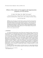
<b>The X-ray diffraction (XRD) patterns of the ZnO:Al films and the target are shown in </b>
<b>Fig. 1. The X-ray diffraction shows only 002 peak indicating the strong preferred </b>
<b>orientation, the c-axes of the grains are uniformly perpendicular to the substrate surface.</b>
<b>The energy dispersive X-ray spectroscopy (EDS) analysis shows that the films are </b>
<b>composed of Zn, 0 and A1 elements (Fig. 2).</b>
</div>
<span class='text_page_counter'>(2)</span><div class='page_container' data-page=2>
<i>Studying the structure and some properties of...</i>
8 1<b>The atomic force microscopy (AFM) observation indicates that all the films are very </b>
<b>smooth and have sim ilar morphology independent of the substrate temperature (Fig. 3)</b>
<b>! ' 1 s </b>
<b>1</b>
<b></b>
<b>-il1 </b>
<b>f</b>
<b>F ig .l. XRD patterns of ZnO: A1 </b>
<b>target and film grown on glass </b>
<b>substrate</b>
<b>Fig.2. EDS spectrum of ZnO </b>
<b>film</b>
<b>Fig.3. The AFM image of ZnO: </b>
<b>A] film grown at 400°c</b>
<b>The resistivity of ZnO films shows very little dependence on temperature (Fig.4). It </b>
<b>can be observed that the resistivity of ZnO: A1 increases slightly with decreasing </b>
<b>temperature. The weak temperature dependence of the resistivity confirms that the A1 </b>
<b>doped ZnO films are degenerate semiconductors.</b>
<b>The resistivities of the films depend on the composition of the target. Figure 5 gives </b>
<b>the film resistivities as a function of A120 3 contents in the target. For the Al-doped ZnO </b>
<b>films, A1 behaves as shallow level n-type dopant. A1 atoms are incorporated in the samples </b>
<b>substitutionally; creating more free electrons and making the sam ples become more </b>
<i><b>conductive. However, when A1 contents are more than the lim it (here it is 3 wt. % for A120 3), </b></i>
<b>the excess A1 atom s behaving as scattering centers in the films, reduce th e mobility of </b>
<b>charge carriers and, subsequently, increase the resistivity of the films.</b>
<b>Figure 6 gives the transmission spectra for three films which have transmission </b>
<b>coefficient of over 80% in the wavelength range of 450-800 nm. The optical gaps were </b>
<b>obtained by plotting (ahv)2 vs. hv (a is the absorption coefficient and hv is the photon </b>
<b>energy) and extrapolating th e straight-line portion of this plot to the energy axis. These </b>
<b>plots yield band gaps of 3.50-3.60 eV.</b>
<b>;</b> <b></b>
<b>---Ỵ</b>
<b>1</b>
<b>.</b> <b>/</b>
<i>r</i>
<b>I</b> <b>»</b>
<b>Nhiệiđộ(K)</b>
<b>Fig.4. The plot of logarithm of </b>
<b>the resistivity vs. temperature </b>
<b>for ZnO: A] film</b>
<b>Fig.5. Electrical resistivities </b>
<b>as a function of A1 contents</b>
<b>Fig.6. The optical transmission </b>
<b>spectra for three highly </b>
<b>conducting ZnO'.Al films with </b>
</div>
<span class='text_page_counter'>(3)</span><div class='page_container' data-page=3>
8 2
<i>Ngo Thu Huong) Ta Dinh Canh,..</i>
<b>evident from the figure that the intensity of the sharp line observed at 3.369 eV is decreased </b>
<b>rapidly and is shifted slightly to the low-energy side with increasing measuring </b>
<b>temperature. At 100 K this line disappears, whereas the line at 3.315 eV is still maintained </b>
<b>up to room temperature. This line is broadened and located at 3.26 eV at 300K. The wide </b>
<b>line peaked at 3.228 eV is shifted to low-energy side with increasing temperature. At 100K </b>
<b>this line is located at 3.046 eV, that is, the shift in energy is about 182 meV. Under such </b>
<b>conditions a new line exhibits at 3.245 eV.</b>
<b>The investigation of the relationship between </b>
<b>the integrated PL intensity vs, temperature shows </b>
<b>that the temperature dependence of th e intensity of </b>
<b>the emission lines at 3.369 and 3.315 eV can be </b>
<i><b>expressed by the equation: I (T) = 10 / [1 + A exp (- E I </b></i>
<b>kBT)], where E is the activation energy of the </b>
<b>thermal quenching process, kB is Boltzman constant,</b>
<b>10 is the emission intensity at 0 K and A is a </b>
<b>constant. For the em ission lines at 3.369 and 3.315 </b>
<b>eV, E = 13.1 and 41.5 meV, respectively.</b>
<b>The strong sharp line at 3.369 eV with </b>
<b>linewidth of 20 meV probably corresponds to </b>
<b>emission of a neutral donor-bound exciton (DoX). The value of 13.1 meV of the activation </b>
<b>energy of the thermal quenching process for this line is close to the normal value of the </b>
<b>binding energy of an exciton bound to a neutral donor. The line at 3.315 eV in our sample </b>
<b>can not be interpreted as two-electron transition of exciton bound to neutral donor, because </b>
<b>this line still remains at the temperatures, at which the bound exciton line disappears. The </b>
<b>line at 3.315 eV can not be attributed to exciton bound to neutral acceptor because of th e low </b>
<b>binding energy for this complex. The excitons are thermally detached from these centers at </b>
<b>low temperatures. The line at 3.315 eV with linewidth as narrow as the bound exciton line is </b>
<b>not due to donor-acceptor pairs because in the last case, the transition energy strongly </b>
<b>depends on the donor-acceptor distance and we should observe a broad emission line. In our </b>
<b>opinion the line at 3.315 eV probably corresponds to recombination o f a free carrier with a </b>
<b>carrier bound on an impurity. In our case, it is possible that recombination of an electron </b>
<b>bound on a donor with a free hole in valence band (BF). The line at 3.228 eV is due to </b>
<b>donor-acceptor pairs (DAP). The line at 3.245 eV is assigned to a longitudinal optical (LO) </b>
<b>phonon replica of BF em ission, because their energy separation is found to be about 70 meV, </b>
<b>which is close to the energy of the LO-phonon.</b>
<b>Fig.7. The PL of ZnO: A] films </b>
measured at temperature ranging
</div>
<span class='text_page_counter'>(4)</span><div class='page_container' data-page=4>
<i>Studying the structure and some properties of...</i>
8 3<b>4. C o n c lu sio n s</b>
<b>Good transparent conducting ZnO:Al films were prepared by r.f. magnetron </b>
<b>sputtering. There is an optimum A]20 3 content with which the films have the highest </b>
<b>conductivity. The photoluminescence spectra at 11-300K show em ission bands related to the </b>
<b>neutral donor-bound exciton, donor-acceptor pairs and transitions from shallow donors to </b>
<b>valence band.</b>
<i><b>Acknow ledgem ents. The authors would like to thank to the Center for Materials Science </b></i>
<b>(CMS), Faculty of Physics, University of Science, Hanoi National University for permission </b>
<b>to use equipment.</b>
<b>R e fer en ces</b>
<b>1. </b> <b>D. H. Zhang, T. H. Yang, J. Ma, Q. p. Wang, R. w . </b>Gao, <b>H. L. </b>M a , <i>A p plied Surface </i>
<i><b>Science, 158(2000) 43.</b></i>
<b>2. </b> <i><b>Ma Jin, Ji Feng, Zhang Deposition-heng, Ma Hong-Lei, Li Shu-ying, T h in S o lid film s, </b></i>
<b>357(1999) 98.</b>
</div>
<!--links-->