bộ điều khiển khả trình LIYAN
Bạn đang xem bản rút gọn của tài liệu. Xem và tải ngay bản đầy đủ của tài liệu tại đây (11.03 MB, 145 trang )
LIYAN PROGRAMMABLE LOGIC CONTROLLER
LYPLC
Ex1 Ex2
USER’S MANUAL
1. Specifications
1 - 1
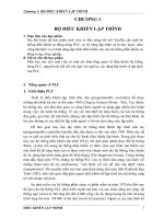
Master Unit & Expansion Unit
Master unit, Expansion I/O unit, Expansion module and EXADP communication module all can assembly to
(35mm)
Open connector cover, connected master unit and expansion i/o unit or expansion module.
Open connector cover, connected master unit and EXADP communication module.
is the LED monitor of input relay, output relay, power, run status and error status.
is the terminal of input relay, is the terminal of output relay.
is EEPROM card.
EX - 32 M R -
No Mark:AC110/220V, D : DC24V
Type of output: R: Relay, T: Transistor
M: Master , E: Expansion
I/O points (16,24,32)
No Mark or 1n : can expansion, 1s: can’t expansion,
Series name
Dimension (mm)
A B C
8
7
130
140
80
90
39.6
48
70
80
EXADP
Master
Expansion I/O
LIYAN ELECTRIC
LYPLC
1. Specifications
1 - 2
Performance Specification
ITEM Ex1s Ex1n
Operating control method Cyclic operation by stored program
I/O control method Batch processing method (when END instruction is executed)
Operation time Basic instruction 0.5us, Applied instruction from 2us to several 100us.
Programming language Relay symbolic language + Step ladder
Program capacity / memory 8000 steps ( built in EEprom )
Number of instruction Basic instruction : 27, Step ladder instruction : 2, Applied instruction : 89.
Input Relay Ex1s:X00~X17, Ex1n:X000 ~ X177 (Sink/Source DC24V 7mA photo coupler isolation)
Output Relay Ex1s:Y00~Y17, Ex1n:Y000 ~ Y177 (Relay : AC250V/1A or Transistor : DC30V/0.5A)
Latched M000 ~ M499 ( EEprom backup ) M000 ~ M499 ( EEprom backup )
General M500 ~ M1535 (no backup) M500 ~ M1535 (no backup)
Auxiliary
Relay
(M)
Special M8000 ~ M8255 (no backup) M8000 ~ M8255
(no backup)
Latched S000 ~ S499
( EEprom backup ) S000 ~ S499
( EEprom backup )
State Relay
(S)
General S500 ~ S999 (no backup) S500 ~ S999 (no backup)
100 msec T000 ~ T199 (no backup) T000 ~ T199 (no backup)
10 msec T200 ~ T245
(no backup) T200 ~ T245
(no backup)
1 ms integration 4 points, T246 ~ T249 (EEPROM backup) 4 points, T246 ~ T249 (EEPROM backup)
100 ms integration 6 points, T250 ~ T255 (EEPROM backup) 6 points, T250 ~ T255 (EEPROM backup)
Timer (T)
Analog 2 points (Define by user) 2 points (Define by user)
Latched C00 ~ C31 (EEprom backup)
Latched C00 ~ C31 (EEprom backup)
16bits Counter
General C32 ~ C199 General C32 ~ C199
General C200 ~ C215 General C200 ~ C215
32bits
Counter
Latched C216 ~ C255 (EEprom backup) Latched C216 ~ C255 (EEprom backup)
6 points : X0 ~ X5 ; X0 or X1 for 1 phase 60KHz , X2 ~ X5 for 1phase 10KHz
Counter (C)
High Speed
Counter
X0 and X1 for 2 phase 30KHz , X2 ~ X5 for 2phase 5KHz
Latched D000 ~ D255 (EEprom backup)
General D256 ~ D3999 (can used FNC(12) MOV stored at EEPROM)
Data Register
Special D8000 ~ D8255 (no backup)
Index V0 ~ V7, Z0 ~ Z7
JMP,CALL P000 ~ P127
Pointer (P)
Pointer (
I
)
Interrupt ( I ) I0xx ~ I8xx
Nest Nest (N) N0 ~ N7
Communication Interface
The 2-nd port (Option)
RS-232C & RS-232C/RS-422,RS-485 RS-232C & RS-232C/RS-422,RS-485
Calendar (Option) Week, Year, Month, Day, Hour, Minute, Second
16 bits: -32,768 ~ +32,767
Constant(K) Decimal
32 bits: -2,147,483,648 ~ +2,147,483,647
16 bits: 0000h ~ FFFFh
Constant(H) Hexadecimal
32 bits: 00000000h ~ FFFFFFFFh
General Specification
Item Description
Source Voltage AC 85~264 V 50/60 Hz
Supply current 24VDC / 800 mA
Momentary power failure Keep operation in 10 ms
Breakdown voltage AC1500/1min (between output terminal and frame ground terminal)
Isolation resistance
DC500v/5mΩ
Noise Impedance Noise voltage: 1000Vp-p, noise width: 1 us
Grounding Class 3 ground
Ambient Temperature
0 ~ 55°
Ambient humidity 35 ~ 85 RH (without condensation)
Atmosphere Must be free from corrosive gasses
1. Specifications
1 - 3
Input Specification
Item DC input (Sink) DC input (Source)
Circuit
Input voltage DC24V+10%, -15% DC24V+10%, -15%
Input current 7mA / DC24V 7mA / DC24V
Impedance
3.3 KΩ 3.3 KΩ
Response
About 10 ms (X00~X07 High Speed) About 10 ms (X00~X07 High Speed)
Input pattern No voltage contact or NPN open collector No voltage contact or PNP open collector
Circuits
Photo coupler Photo coupler
Output Specification
Item Relay output Transistor output
Circuit
Load voltage Under AC250V DC30V DC5V ~ 30V
Rated current 2A / 1 point 0.5A / 1 point
Rated capacity
Response time About 10ms Under 1 ms
Circuits
Machine isolation Photo coupler
Note of Output Specification
Ex1s Ex1n Transistor output module haven’t pull high resistor 2.2K
EX32MT-P Transistor output module have pull high resistor 2.2K
VCC
24V
24G
S/S
X00
VCC
24V
24G
S/S
X00
Y0
CO
RY
Y0
CO
TRIGGER
1. Specifications
1 - 4
Source Power Wiring Diagram ( NPN Mode )
AC85 ∼264V 50/60Hz
LX NX
• •
24V S/S 24G X0
… …
X17
Master Unit (MR type)
24V 24G
• •
C0 Y0 Y1 Y2 Y3
… …
Y17
load
Source Power Wiring Diagram ( PNP Mode )
AC85 ∼264V 50/60Hz
LX NX
• •
24V S/S 24G X0
… …
X17
DL
MC
GND
5V
DC/DC
1. Specifications
1 - 5
16MR Type Terminal Signal ( Sink/Source set by internal, manufacture preset Sink NPN mode )
AC85 ∼264V 50/60Hz
NX FG LX COM X00 X01 X02 X03 X04 X05 X06 X07
PLC
24V 24G C0 Y00 Y01 Y02 Y03 C1 Y04 Y05 Y06 Y07
14MT Type Terminal Signal and Wiring Diagram ( Internal Power Used )
AC85 ∼264V 50/60Hz
NX FG LX COM X00 X01 X02 X03 X04 X05 X06 X07
PLC
24V 24G 24I CA0 Y00 Y01 CA1 Y02 Y03 C1 Y04 Y05
*option *option
24V 24G pulse
…. ….
sign
…. …. …. ….
Servo Driver
14MT Type Terminal Signal and Wiring Diagram ( External Power Used )
AC85 ∼264V 50/60Hz
NX FG LX COM X00 X01 X02 X03 X04 X05 X06 X07
PLC
24V 24G 24I CA0 Y00 Y01 CA1 Y02 Y03 C1 Y04 Y05
*option *option
24V 24G pulse
…. ….
sign
…. …. …. ….
Servo Driver
1. Specifications
1 - 6
24MR Type terminal Signal ( 24V – S/S = NPN Mode, 24G – S/S = PNP Mode )
AC85 ∼264V 50/60Hz
NX FG LX
•
•
24V S/S 24G X00 X01 X02 X03 X04 X05 X06 X07 X10 X11 X12 X13 X14 X15 X16 X17
PLC
24V 24G
•
•
C0 Y00 Y01 Y02 Y03 C1 Y04 Y05 Y06 Y07
•
•
•
•
•
•
•
•
•
•
24MT Type Terminal Signal and Wiring Diagram ( Internal Power Used )
AC85 ∼264V 50/60Hz
NX FG LX
•
•
24V S/S 24G X00 X01 X02 X03 X04 X05 X06 X07 X10 X11 X12 X13 X14 X15 X16 X17
PLC
24V 24G 24I CA0 Y00 Y01 CA1 Y02 Y03 C1 Y04 Y05 Y06 Y07
•
•
•
•
•
•
•
•
•
•
*option *option
24V 24G pulse
….
….
sign
….
….
….
….
….
….
….
….
….
….
….
….
….
….
….
….
Servo Driver
24MT Type Terminal Signal and Wiring Diagram ( External Power Used )
AC85 ∼264V 50/60Hz
NX FG LX
•
•
24V S/S 24G X00 X01 X02 X03 X04 X05 X06 X07 X10 X11 X12 X13 X14 X15 X16 X17
PLC
24V 24G 24I CA0 Y00 Y01 CA1 Y02 Y03 C1 Y04 Y05 Y06 Y07
•
•
•
•
•
•
•
•
•
•
*option *option
24V 24G pulse
….
….
sign
….
….
….
….
….
….
….
….
….
….
….
….
….
….
….
….
Servo Driver
1. Specifications
1 - 7
32MR Type Terminal Signal ( 24V – S/S = NPN Mode, 24G – S/S = PNP Mode )
AC85 ∼264V 50/60Hz
NX FG LX
•
•
24V S/S 24G X00 X01 X02 X03 X04 X05 X06 X07 X10 X11 X12 X13 X14 X15 X16 X17
PLC
24V 24G
•
•
C0 Y00 Y01 Y02 Y03 C1 Y04 Y05 Y06 Y07 C2 Y10 Y11 Y12 Y13 C3 Y14 Y15 Y16 Y17
32MT Type Terminal Signal and Wiring Diagram ( Internal Power Used )
AC85 ∼264V 50/60Hz
NX FG LX
•
•
24V S/S 24G X00 X01 X02 X03 X04 X05 X06 X07 X10 X11 X12 X13 X14 X15 X16 X17
PLC
24V 24G 24I CA0 Y00 Y01 CA1 Y02 Y03 C1 Y04 Y05 Y06 Y07 C2 Y10 Y11 Y12 Y13 C3 Y14 Y15 Y16 Y17
*option *option
24V 24G pulse
….
….
sign
….
….
….
….
….
….
….
….
….
….
….
….
….
….
….
….
Servo Driver
32MT Type Terminal Signal and Wiring Diagram ( External Power Used )
AC85 ∼264V 50/60Hz
NX FG LX
•
•
24V S/S 24G X00 X01 X02 X03 X04 X05 X06 X07 X10 X11 X12 X13 X14 X15 X16 X17
PLC
24V 24G 24I CA0 Y00 Y01 CA1 Y02 Y03 C1 Y04 Y05 Y06 Y07 C2 Y10 Y11 Y12 Y13 C3 Y14 Y15 Y16 Y17
*option *option
24V 24G pulse
….
….
sign
….
….
….
….
….
….
….
….
….
….
….
….
….
….
….
….
Servo Driver
1. Specifications
1 - 8
16EX Type Terminal Signal ( 24V – S/S = NPN Mode, 24G – S/S = PNP Mode )
•
24V S/S 24G X00 X01 X02 X03 X04 X05 X06 X07
PLC
•
24V S/S 24G X10 X11 X12 X13 X14 X15 X16 X17
16ER, 16ET Type Terminal Signal ( 24V – S/S = NPN Mode, 24G – S/S = PNP Mode )
•
24V S/S 24G X00 X01 X02 X03 X04 X05 X06 X07
PLC
• •
C0 Y00 Y01 Y02 Y03 C1 Y04 Y05 Y06 Y07
24ER, 24ET Type Terminal Signal ( 24V – S/S =NPN Mode, 24G – S/S = PNP Mode )
•
•
•
•
•
24V S/S 24G X00 X01 X02 X03 X04 X05 X06 X07 X10 X11 X12 X13 X14 X15 X16 X17
PLC
•
•
•
•
C0 Y00 Y01 Y02 Y03 C1 Y04 Y05 Y06 Y07
•
•
•
•
•
•
•
•
•
•
32ER, 32ET Type Terminal Signal ( 24V – S/S = NPN Mode, 24G – S/S = PNP Mode )
•
•
•
•
•
24V S/S 24G X00 X01 X02 X03 X04 X05 X06 X07 X10 X11 X12 X13 X14 X15 X16 X17
PLC
•
•
•
•
C0 Y00 Y01 Y02 Y03 C1 Y04 Y05 Y06 Y07 C2 Y10 Y11 Y12 Y13 C3 Y14 Y15 Y16 Y17
1. Specifications
1 - 9
8EX Type Terminal Signal
24V 24G X00 X01 X02 X03
PLC
24V 24G X04 X05 X06 X07
8ER, 8ET Type Terminal Signal
24V 24G X00 X01 X02 X03
PLC
•
C0 Y00 Y01 Y02 Y03
8EYR, 8EYT Type Terminal Signal
•
C1 Y04 Y05 Y06 Y07
PLC
•
C0 Y00 Y01 Y02 Y03
485ADP Type Terminal Signal
24V FG 24G
•
•
•
PLC
RDA RDB SDA SDB SG SG
2DA Type Terminal Signal
24V FG 24G
•
•
•
PLC
V1 I1 C1 V2 I2 C2
2AD Type Terminal Signal
24V FG 24G
•
•
•
PLC
V1 I1 C1 V2 I2 C2
2AD-LD Type Terminal Signal
24V FG 24G
•
•
•
PLC
+5V L1- L1+ -5V L2- L2+
8AD Type Terminal Signal
24V FG 24G
•
V1 C1 V2 C2 V3 C3 V4 C4
PLC
V5 I5 C5 V6 I6 C6 V7 I7 C7 V8 I8 C8
1. Specifications
1 - 10
Note for Wiring
♦ Don’t wiring to the mark ( • ) of terminal.
♦ The signal wire of input and output can’t used the
same cable.
♦ Don’t put the signal cable of input and output with
power able at the same tube.
♦ The expansion wire can expansion to 50mm~
100mm. But need avoid noise, so the expansion
wire with the output wire need had Min. 50 mm
space.
♦ Because the expansion module with power device,
so can’t wiring the +24V of expansion module to
the +24V of master. But the expansion I/O unit no
power device, so the +24V of master unit need
connected to the expansion I/O unit.
Expansion
Unit
Master
Unit
Min. 50mm
( 2.0in )
Expansion
Wire
LIYAN ELECTRIC
LYPLC
32MR
LIYAN ELECTRIC
LYPLC
32ER
2. Basic Instructions
List of Basic Instruction
Symbol Function Circuit & Devices
LD
LoaD
Each logic start
A contact
X
,
Y
,
M
,
S
,
T
,
C
LDI
LoaD Inverse
Each logic start
B contact
X
,
Y
,
M
,
S
,
T
,
C
AND
AND
Serial connection
A contact
X
,
Y
,
M
,
S
,
T
,
C
ANI
ANd Inverse
Serial connection
B contact
X
,
Y
,
M
,
S
,
T
,
C
OR
OR
Parallel connection
A contact
X
,
Y
,
M
,
S
,
T
,
C
ORI
OR Inverse
Parallel connection
B contact
X
,
Y
,
M
,
S
,
T
,
C
ANB
ANd Block
Serial connection
of Parallel circuit
ORB
OR Block
Parallel connection
of serial circuit
OUT
OUT
Final operation
coil drive
Y
,
M
,
S
,
T
,
C
LDP
LoaD rising Pulse
Initial logical operation
Rising edge pulse
X
,
Y
,
M
,
S
,
T
,
C
LDF
LoaD Falling pulse
Initial logical operation
Falling edge pulse
X
,
Y
,
M
,
S
,
T
,
C
ANDP
AND Pulse
Serial connection
of Rising edge pulse
X
,
Y
,
M
,
S
,
T
,
C
ANDF
AND Falling
Serial connection
of Falling edge pulse
X
,
Y
,
M
,
S
,
T
,
C
ORP
OR Pulse
Parallel connection
of Rising edge pulse
X
,
Y
,
M
,
S
,
T
,
C
ORF
OR Falling
Parallel connection
of Falling edge pulse
X
,
Y
,
M
,
S
,
T
,
C
NOP
NOP
No operation N/A
PLS
PULSE
Rising edge pulse PLS YM
PLF
PLF
Falling edge pulse
PLF YM
♣
SET
SET
Set a bit device
Permanently ON
SET
YMS
♣
RST
ReSeT
Reset a bit device
Permanently OFF
RST
YMSTCDVZ
MC
Master Control
Denote the start
of Master control block
MC
N YM
MCR
Master Control Reset
Denote the end
of Master control block
MCR N
INV
INVerse
Invert the current result
of the internal PLC operations
MPS
PuSh
Push the result
of operation to stack
MRD
ReaD
Read the result
of operation from stack
MPP
PoP
Pop & remove
the Result from stack
END
END
Main program end
Forced the current program
scan to step 0
MPP
ʘ
MRD
ʘ
ʘ
MPS
♣ : Special Auxiliary Relay
2 - 1
2. Basic Instructions
Load & Load Inverse & Out Instruction
Mnemonic
Instruction Symbol & Device Step number
LD
LoaD
( )
X,Y,M,S,T
,C
1
LDI
LoaD Inverse
( )
X,Y,M,S,T,C
1
OUT
OUT
( )
Y,M,S,T,C
1
♦ If each logic line start an NO contact, use the LD instruction.
LD OUT
X0
↙ ↙
LD X 0
(
Y0
)
OUT Y 0
♦ If each logic line start an NC contact, use the LDI instruction.
LDI OUT
LDI X 1
X1
↙ ↙
OUT Y 1
(
Y1
)
OUT T 0
(
T0
)
K 50
(SP)
K 50
♦ When using hand held programmer the space key needs to be pressed to enable the constant to be entered.
AND & AND Inverse Instruction
Mnemonic
Instruction
Symbol & Device Step number
AND
AND
( )
X,Y,M,S,T
,C
1
ANI
ANd Inverse
( )
X,Y,M,S,T,C
1
♦ If an NO contact is connected in series, use the AND instruction.
AND
X2 X3
↙
LD X 2
(
Y2
)
AND X 3
OUT Y 2
♦ If an NC contact is contacted in series, use the ANI Instruction.
ANI
X2 X3
↙
LD X 2
( Y3 )
ANI X 3
OUT Y 3
X0
LD X 0
( Y0 )
OUT Y 0
X1
AND X 1
( Y1 ) OUT Y 1
EX EX
1S
EX
1N
EX
2N
EX EX
1S
EX
1N
EX
2N
2 - 2
2. Basic Instructions
OR & OR Inverse Instruction
Mnemonic
Instruction
Symbol & Device Step number
OR
OR
( )
X,Y,M,S,T,C
1
ORI
OR Inverse
( )
X,Y,M,S,T,C
1
♦ If an NO contact is connected in parallel, use the OR instruction.
X4
LD X 4
(
Y4
)
OR X 5
X5 ←
OR
OUT Y 4
♦ If an NC contact is connected in parallel, use the ORI instruction.
X4
LD X 4
(
Y4
)
ORI X 5
X5 ←
ORI
OUT Y 4
ANB Instruction
Mnemonic
Instruction
Symbol & Device Step number
ANB
ANd Block
( )
N/A
1
♦ Serial connection of parallel circuit, use the ANB
X10 X12 LD X 10
( Y10 ) OR X 11
X11 X13
LD X 12
OR X 13
ANB
OUT Y 10
ORB Instruction
Mnemonic
Instruction
Symbol & Device Step number
ORB
OR Block
( )
N/A
1
♦ Serial connection of parallel circuit, use the ORB
X10 X12 LD X 10
(
Y11
)
AND X 12
X11 X13 LD X 11
←
ORB
AND X 13
ORB
EX EX
1S
EX
1N
EX
2N
EX EX
1S
EX
1N
EX
2N
EX EX
1S
EX
1N
EX
2N
OUT Y 11
2 - 3
2. Basic Instructions
Load Pulse & Load Falling Pulse Instruction
Mnemonic
Instruction
Symbol & Device Step number
LDP
LoaD rising Pulse
X,Y,M,S,T,C 2
LDF
LoaD Falling pulse X,Y,M,S,T,C
2
" 0 LDP X 0
2 OR X 1
3 OUT M 100
" 4 LDF X 0
6 OUT Y 0
LDF
↙
LDP
↙
X0
X0
X1
Y0
M100
EX
EX
1S
EX
1N
EX
2N
Basic points to remember:
♦ Connect the LDP and LDF instructions directly to the left hand bus bar.
♦ Or use LDP and LDF instructions to define a new block of program when using the ORB and ANB instructions
(see later sections).
♦ LDP is active for one program scan after the associated device switches from OFF to ON.
♦ LDF is active for one program scan after the associated device switches from ON to OFF.
Single Operation flags M2800 to M3071
♦ The pulse operation instructions, when used with auxiliary relays M2800 to M3071, only activate the first
instruction encountered in the program scan, after the point in the program where the device changes. Any other
pulse operation instructions will remain inactive.
♦ This is useful for use inn STL programs (see chapter 3) to perform single step operation using a single device.
♦ Any other instructions (LD, AND, OR, etc.) will operate as expected.
2 - 4
2. Basic Instructions
AND Pulse & AND Falling Pulse Instruction
Mnemonic
Instruction
Symbol & Device Step number
ANDP
AND Pulse
X,Y,M,S,T,C 2
ANDF
AND Falling pulse X,Y,M,S,T,C
2
0 LD M 40
1 OR X 1
"
2 ANDP T 10
4 OUT M 100
5 LDF X 0
"
6 ANDF C 0
8 OUT Y 4
C0
T10
ANDF
↙
ANDP
↙
X0
X1
M40
Y4
M100
EX EX
1S
EX
1N
EX
2N
Basic points to remember:
♦ Use the ANDP and ANDF instructions for the serial connection of pulse contacts.
♦ Usage is the same as for AND and ANI; see earlier.
♦ ANDP is active for one program scan after the associated device switches from OFF to ON.
♦ ANDF is active for one program scan after the associated device switches from ON to OFF.
Single operation flags M2800 to M3071:
♦ When used with flags M2800 to M3071 only the first instruction ill activate.
2 - 5
2. Basic Instructions
OR Pulse & OR Falling Pulse Instruction
Mnemonic
Instruction
Symbol & Device Step number
ORP
OR Pulse
X,Y,M,S,T,C 2
ORF
OR Falling pulse X,Y,M,S,T,C
2
0 LD M 40
"
1 ORP X 1
3 SET M 50
4 LD X 0
5 AND M 24
6 LD Y 7
"
7 ORF X 1
9 ORB
10 OUT Y 4
ORF
M40
X1
X0 M24
Y7 X1
Y4
ORP
SET M50
EX EX
1S
EX
1N
EX
2N
Basic points to remember:
♦ Use the ORP and ORF instructions for the parallel connection of pulse contacts.
♦ Usage is the same as for OR and ORI; see earlier.
♦ ORP is active for one program scan after the associated device switches from OFF to ON.
♦ ORF is active for one program scan after the associated device switches from ON to OFF.
Single operation flags M2800 to M3071
♦ When used with flags M2800 to M3071 only the first instruction will activate.
2 - 6
2. Basic Instructions
NOP & END Instruction
EX EX
1S
EX
1N
EX
2N
Mnemonic
Instruction
Symbol & Device Step number
NOP
NOP
N/A
1
END
END END
1
NOP Instruction
♦ After the program ‘all clear operation’ is executed, all of instructions in the program are over written with NOP’s.
END INSTRUCTION
♦ Insert this instruction at the end of a program and the program return to step 0.
♦ If missing this instruction then program can’t be executed
NOTE :
1:Program a circuit from its up to down and left to right.
2:Output relay can’t be connected directly from the bus bar.
If necessary connect it through the N/C contact of special auxiliary relay M8000.
3:I/O relay, inside auxiliary relay, TIM/OUT the number of contact that can be used per output relay is not limited.
4:Behind the output coil can not in addition contact; Two or more output coils can be connected in parallel.
2 - 7
2. Basic Instructions
Multiplex output circuit
EX EX
1S
EX
1N
EX
2N
Mnemonic
Instruction Symbol & Device Step number
MPS
Memory PuSh 1
MRD
Memory ReaD 1
MPP
Memory PoP
( )
( )
MPS
MRD
( )
MPP
1
♦ LYPLC EX series has (11) stack memory space can stores operation result, so MPS instruction may be used up
to
(11) times continuously.
♦ MPS: Push the operation result into stack and the stack pointer increment by 1.
♦ MRD: Read the operation result from stack and the stack pointer unchanged.
♦ MPP: Pop the operation result from stack. First the stack pointer decrement by 1.
♦ MPS,MRD,MPP are all no operand.
LD X 00
X00 OUT Y 00
( Y00 ) AND X 01
X01 OUT Y 01
( Y01 ) LD X 02
X02
MPS
X03 MPS
( Y02 ) AND X 03
X04 OUT Y 02
( Y03 ) MPP
X10 MPP X11 AND X 04
( Y04 ) OUT Y 03
MPS X12 LD X 10
( Y05 ) MPS
MRD
X13 AND X 11
( Y06 ) OUT Y 04
MRD
X14 MRD
( Y07) AND X 12
MPP
OUT Y 05
ʘ
ʘ
ʘ
ʘ
ʘ
ʘ
ʘ
MRD
AND X 13
OUT Y 06
MPP
AND X 14
OUT Y 07
2 - 8
2. Basic Instructions
Master Control ( MC/MCR )
Mnemonic
Instruction
Symbol & Device Step number
MC
Master control
MC N Y,M
2
MCR
Master Control Reset MCR N
1
X10 LD X 10
MC N0 M10 MC N 0
N0 M10 SP M 10
X 1 LD X 1
( Y0 ) OUT Y 0
X 2 LD X 2
( Y1 ) OUT Y 1
MCR N0 MCR N 0
EX EX
1S
EX
1N
EX
2N
♦ N is the nesting level number.
♦ The MC/MCR instruction are used in pairs when branching a circuit to plural OUT instruction.
♦ When the MC condition is ON, the state of each relay is the same as in an ordinary circuit with out MC/MCR
instruction.
♦ When the MC condition is OFF, the state of each relay between the MC and MCR instruction is as following:
Time, Device for OUT Reset & OFF
Counter, Device for SET Hold present state
♦ Be sure that an LD/LDI instruction will always following the MC/MCR instruction.
2 - 9
2. Basic Instructions
Inverse ( INV )
EX EX
1S
EX
1N
EX
2N
Mnemonic
Instruction
Symbol & Device Step number
INV
INVerse
N/A 1
0 LD X 0
" 1 PLS M 0
3 LD M 0
4 SET Y 0
5 LD X 1
" 6 PLF M 1
8 LD M 1
X0
M0
X1
M1
Y0 RST
M1 PLF
Y0 SET
PLS M0
9 RST Y 0
Basic points to remember:
♦ The INV instruction is used to change (invert) the logical state of the current ladder network at the inserted
position.
♦ Usage is the same as for AND and ANI; see earlier.
Usages for INV
♦ Use the invert instruction to quickly change the logic of a complex circuit.
It is also useful as an inverse operation for the pulse contact instruction LDP, LDF, ANP, etc.
2 - 10
2. Basic Instructions
PLS / PLF (Pulse Output)
Mnemonic
Instruction
Symbol & Device Step number
PLS
PuLSe
PLS
Y. M .
2
PLF
PuLse Falling
PLF
Y. M. 2
X0 LD X 0
PLS Y0 PLS Y 0
X1
LD X 1
PLF Y1 PLF Y 1
X0 ♦ When X0 pulse OFFON the specified devices of PLS is enabled “1” scan
cycle.
Y0
X1 ♦ When X1 pulse ONOFF the specified devices of PLF is enabled “1” scan
cycle.
Y1
♦ The special auxiliary relay can’t for PLS/PLF used.
SET/RST
Mnemonic
Instruction
Symbol & Device Step number
SET
SET
SET
Y, M , S
Y.M. :1
Special M,S
Coils :2
RST
ReSeT
RST
Y, M, S, D
D, special
D, registers,
V and Z :3
X0 LD X 0
SET Y0 SET Y 0
X1
LD X 1
RST Y0 RST Y 0
X0
X1
Y0
EX EX
1S
EX
1N
EX
2N
EX EX
1S
EX
1N
EX
2N
♦ SET : While the operation result is on the specified device is enabled. Once enabled, the specified device
remains enabled even if the operation result is disabled.
♦ RST : While the operation result is on the specified device is reset, word device cleared to “0”.
2 - 11
2. Basic Instructions
TIMER & COUNTER
EX EX
1S
EX
1N
EX
2N
Mnemonic
Instruction
Symbol & Device Step number
OUT
OUT
( T.C ) K
32 bit
counter : 5
Others :3
RST
RST
RST
T,C T.C : 2
<< Timer >>
X0 LD X 0
( T0 ) OUT T 0
T0
K50
K 50
( Y0) LD T 0
OUT Y 0
X0
♦ When X0 on, T0 active after 5 seconds T0 contact ON, and keep current data
even through X0 keep ON.
T0
coil
5 sec
T0 contact
♦ When X0 off, then clear T0 to “0” and contact off,
Y0
♦ Timer can be set directly by using constant K or indirectly by using data register
(D).
(
T0
)
D0
♦ All of the timers (T000~T255) are unlatched.
<< Counter >>
X0 LD X 0
RST C0 RST C 0
X1
LD X 1
( C0 ) OUT C 0
C0
K5
K 5
( Y0 ) LD C 0
OUT Y 0
X0
X1
C0
♦ When X0 ON, clear C0 current data to“0” and contact off.
♦ C0 count up the signal of X1 (OFFON), after 5 counts then keep current value and the contact ON.
♦ Counters can be set directly using constant K or indirectly by using data register (D).
( C0 ) D0
♦ All of the counters ( C0 ~ C255 ) are latched.
♦ The high speed counters reference chapter 4.
2 - 12
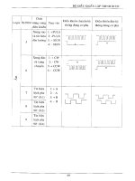
3. Step Ladder Instructions
How STL Operates
3 - 1 The state activate & move condition
A ( Y0 ) A A
SET Y1
X0 Å move condition X0 X0
B ( Y2 ) B B
( 3-1a ) ( 3-1b ) ( 3-1c )
♦ When (3-1a) state A ON,then executing the program belonged to state A, i.e. Y0 ON, Y1 ON, Y2 OFF. State B
OFF, the program belonged to state B not executing.
♦ When move condition X0 ON (don’t need keep), then state B ON, i.e. state A ON and state B ON in one cycle
time (3-1b) Y0,Y1,Y2 all ON.
♦ After one cycle state A auto OFF, state B still ON (3-1c) i.e. Y0 OFF, Y1 ON (SET), Y2 ON.
♦ Once the current STL state activates a second following state, the source STL state will auto reset,
3 - 2 Simple Flow Chart (SFC)& Ladder Chart (STL)
S1
S1 ( Y0 ) ( Y0 )
X0 Åmove condition
X0 Å move condition SET S2
S2 S2 is move destination
S2 move destination
( 3-2a ) Simple Flow Chart -SFC ( 3-2b ) Ladder - STL
♦ ( 3-2a ) is Simple Flow Chart, ( 3-2b ) is Ladder Chart.
♦ The state (S) can be connected to Output Relay directly.
♦ To Activate an STL state, need drive the STL coil first.
In the EX-series, the SET is used to drive an STL state to make it active.
♦ The formula is used M8002 & ZRST to initial STL state, and used M8002 & SET to start STL program.
♦ The RET instruction is end of STL state, let program return to ladder sequence.
3 - 1
3. Step Ladder Instructions
3 - 3 STL&RET Operands : S0 ∼ S999
3 – 3 – 1 : Single Flow Mode
M8002 M8002
S0 ( Y 10 )
SET S0
SET Y11 S0
( T10 ) ( Y10 )
T10
K50
SET Y11
S1 ( Y12 )
( T10 )
( T11 ) T10
K50
T11
K30
SET S1
S2 RST Y11 S1
( Y13 ) ( Y12 )
( T12 )
( T11 )
T12
K20
T11
K30
S0 RET SET S2
S2
RST Y11
( Y13 )
( T12 )
T12
K20
SET S0
RET
Fig 3-3-1a
Simple Flow Chart - SFC Fig 3-3-1b. Ladder - STL
LD M 8002
K 30
SET S 0 LD T 11
STL S 0 SET S 2
OUT Y 10 STL S 2
SET Y 11 RST Y 11
OUT T 10 OUT Y 13
K 50 OUT T 12
LD T 10 K 20
SET S 1 LD T 12
STL S 1 SET S 0
OUT Y 12 RET
OUT T 11
♦ The end of STL program area need added RET instruction, let program return to original bus bar.
3 - 2