MOSFET MODELING FOR VLSI SIMULATION - Theory and Practice Episode 6 pptx
Bạn đang xem bản rút gọn của tài liệu. Xem và tải ngay bản đầy đủ của tài liệu tại đây (1.53 MB, 40 trang )
176
5
Threshold Voltage
3.0
2.0
-
>
w
0
z
0
20
=!
u
2
1.0
u)
>-
-I
2
-1.0
2
-2.0
+c
a
f
>
-3.0
I
014
4.0
-
3.0
3
w
0
2
0
2
i
2
2.0
1.0
?I
0
+*
2
-1.0
>-
0
a.
K
L
SUBSTRATE
DOPING,
Nb
(
~m-~
)
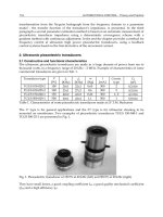
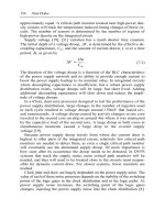
Fig.
5.5
Calculated threshold voltage
V,,
for
n-
and p-channel MOSFETs
as
a
function of
substrate doping
N,
for
n+
polysilicon gate (left scale)
and
p+
polysilicon gate (right scale)
for
three different oxide thickness. (After Sze
[5])
curves are based on the assumption that
Qo
=
0,
a reasonable assumption
for modern
VLSI
processes.
The temperature through the
4f
term,
the higher the temperature, the
lower
the
Vlh
(for details see section 5.4)
The body bias
Vsb;
the higher the
Vsb,
the higher the
Vfh.
The increase in
Vth
due to an increase in
V,,
can be obtained from
Eq.
(5.16)
as
(5.17)
Avfh
=
vfh
-
vTO
=
Y[Jm
-
61.
Body-EfSect.
The variation of
v,h
with
v,,
is
often called the
substrate bias
sensitivity
or
body-efSect.
Differentiating
Eq.
(5.14) with respect to
V,,
we
get
(5.18)
where the
+
and the
-
signs are for
n-
and p-channel devices, respectively.
This equation shows that the body-effect increases as the body factor
y
Y
f
dvfh
-
"sb
2Jm
5.2
Nonuniformly Doped MOSFET
111
increases and body bias
V,b
decreases. For circuit design,
it
is often desirable
to lower the body effect,3 which means the body factor
y
should be reduced.
From Eq. (5.1
1)
it is evident that
y
can be reduced with lower doping con-
centration
N,
and/or lower oxide thickness
tax.
However, lowering
N,,
for
example, conflicts with the scaling rule (cf. section 3.4). In fact, the choice
of process or circuit parameters is a trade
off
between various parameters
involved in device design.
SPICE Implementation.
Note that Eq. (5.14) becomes invalid for
v,b
I
-
24,.,
i.e., when the
S/D
diodes become forward biased by an amount
24,
Although during normal operation of the device the
S/D
diodes will not
be forward biased; however, in SPICE, during Newton-Raphson iterations,
it is possible to encounter
V,,
<
-
24,
This is just an artifact of the iteration
solution process, and convergence to
a
proper solution requires the model
to
behave well even
in
such invalid operating regions. Therefore,
to
use
Eq.
(5.14)
or (5.16) in the forward biased region of
S/D
junction, some sort
of
smoothing function is used to limit the value of
(V,,
+
24f)
such that it
is always positive. The smoothing function assures a smooth transition with-
out any discontinuity. In
SPICE,
the transition point is chosen as
V,,
=
-
4,
Thus, when
V,,
+
4J
2
0,
Eq.
(5.14)
is used and when
V,,
+
4,.
<
0,
the term
Jm
is replaced by
2&/(1
-
Vsb/4f)
such that
V,,,
and its first
derivative are continuous at
V,,
=
-
4f
in the forward biased
S/D
region.
5.2
Nonuniformly
Doped
MOSFET
In the previous section we have seen that for
a
given gate material the
threshold voltage
V,,
of a MOSFET depends upon the substrate doping
concentration
Nb
and the gate oxide thickness
Lox.
Therefore, in principle,
V,,,
could be set
to
any value by proper choice of
Nb
and
fox
(see Figure 5.5).
However, considerations like the body-effect, source-drain junction capaci-
tances and breakdown voltages often dictate desirable values of these
parameters. In practice this is achieved by ion implanting a shallow layer
of dopant atoms into the substrate in the channel region. Thus, by adjusting
the channel surface concentration (using ion implantation) any desired
value of
V,,
can be achieved. In fact, in VLSI devices, more than one
implant is often used in the channel region-one
to
adjust the threshold
voltage and another to avoid the punchthrough effect-as was discussed
~
3
During circuit operation, in NMOS circuits, the MOSFET source voltage often increases
which results in higher
V,,
thereby causing
V,,
to increase.
This
results in a decrease in
the drain current
I,,
[see
Eq.
(3.4)],
consequently the circuit runs at a lower speed and
might not even function properly.
For
this reason,
it
is desirable to reduce the change in
V,,
due to increase in
V,,,
that
is
reduce body-effect.
178
5
Threshold Voltage
in section 3.5.2. The fact that the surface is no longer uniformly doped,
due to the channel implant, means
Eq.
(5.14) is generally not valid.
Recall that in
n+
polysilicon gate CMOS technology, an nMOST has
channel implant dopants (boron) which are of the same type as that of the
substrate (p-type), while pMOST (compensated p-device) has shallow
channel implant dopants, which are of the type opposite to that
of
the
substrate (cf. section 3.5.2). Since compensated pMOST has shallow channel
implant, the surface layer is depleted at zero gate bias. When
Vys
>
I/th,
the current flows at the surface. Therefore, these compensated devices are
usually modeled in the same way as nMOST,
so
far as the drain current
modeling is concerned; however they have a different threshold voltage
model as we will see later. In
a
recent submicron CMOS technology,
pMOSTs are being fabricated with
p+
polysilicon gate while nMOSTs are
with
n+
polysilicon gates. With
p+
polysilicon gate, pMOST has channel
implant of the same type as substrate and therefore, from a modeling point
of
view, these devices are similar to nMOST.
In the depletion type devices the channel implant, which
is
of opposite
type to that of the substrate, is deep
so
that significant current flows even
at
V,,
=
OV.
These (depletion) devices are referred to as normally-on buried
channel (BC) MOSFET as against the compensated devices, which are also
referred to as normally-of
buried
channel (BC) MOSFETs. The two BC
MOSFETs result in entirely different
V,,
behavior due to the different
potential distributions associated with the built-in pn junctions in the
channel region. This can easily be seen from their energy band diagrams
as shown in Figure 5.6 for a p-channel device with a p-type buried layer
in n-type substrate and an
n+
polysilicon gate. While for the normally-off
BC MOSFET (Figure 5.6a) the energy band bending of the bulk junction
extends to the channel surface, the depletion device (normally-on) has an
(hole) energy
minimum
(Figure
5.6b).
It
was pointed out earlier (cf. section
3.5.2) that in practice p-channel depletion devices are not usually made. It
Ec
E
f
Ei
n
E"
(a)
(b)
Fig.
5.6 Energy band diagram
for
a
p-type buried-channel
MOSFET
in
(a)
the surface
channel mode and
(b)
the buried channel mode (depletion device)
5.2
Nonuniformly Doped
MOSFET
179
is the n-channel depletion device, with negative threshold voltage, which
is
more important and thus modeled here.
There is an extensive literature
on
threshold voltage models for ion implanted
devices
[ll-[36].
However, we will discuss and develop only those models
which are suitable for circuit simulators. We will first discuss enhancement
mode devices and then depletion mode devices.
5.2.1
Enhancement Type Device
When ions are implanted into the channel, the implanted profile can be
fairly accurately approximated by the following Gaussian distribution
function (see Figure
5.7,
also see Appendix
H,
Eq.
(H.5))
(5.19)
where
No
=
Di/(ARp&)
is the maximum concentration and occurs at
x
=
R,,
R,
=
projected
range (average penetration depth),
Di
=
dose,
i.e., number of implanted ions per unit area.
x
=
the depth measured from the oxide-silicon interface,
ARp
=
straggle
(standard deviation)
The channel implant dose
Di
is typically
of
the order of
10"
-
1012
cm-2
while the implant energy varies from
10-200
KeV. Following the implantation
process, devices go through various high-temperature fabrication steps,
which change the final profile. Figure
5.8
shows the final channel implant
profiles for nMOST and pMOST for a typical 2pm CMOS technology
with
n+
polysilicon gate.
Fig.
5.7
Gaussian doping profile in the channel region
of
a
VLSI
MOSFET
180
5
Threshold Voltage
0
lo1’
-
ASSUMED DOPING PROFILE
Nb
20
1014
00
05
10 15
DEPTH INTO SILICON,
X
(pm)
(a)
-
-
,
P-N
JUNCTION
-
1014
I I!/:[ I I
I I
I
I
I
I
I
I
I
I
I
I
00
05
10
15
20
DEPTH INTO SILICON,
X
(pm)
(b)
Fig.
5.8
Vertical doping
profile
of channel implanted region under
the
gate for a typical
2
prn
CMOS process for
(a)
nMOST and
(b)
pMOST
The result of the channel implant in an otherwise uniformly doped substrate
is
to
change the threshold voltage. The extrapolated threshold voltage
V,,
as a function
of
Jm
for different channel implant dose
is
shown
in Figure 5.9
[6].
One can see from this figure that
the slope
of
the
V,,
versus
V,,
curve changes from single dope at low doses to two distinct slopes
at higher doses.
This shows that a simple square root dependence, which
relates
V,,
to
Vsb,
is not correct for channel implanted devices with high
doses. However, for these devices Eq.
(5.7)
is still valid provided we use
appropriate value of
Vfbr
4si,
and
Qb(4si).
We will now consider each
of
these terms and see how they are modified for implanted devices.
5.2
Nonuniformly Doped
MOSFET
181
6
4
c
>
u
2
f
>
0
vsb(v)
0.5
0
.2
.4
.6
.8
I
I
I
I
I1
I1
-2
DOSE
=
12
XI0
C
cm
1
SUBSTRATE
P-Si
<I00
>
I
I
I
Fig.
5.9
Threshold voltage dependence on body bias for different channel implants. (After
Kamoshida
[6])
Flat Band Voltage
Vfb.
As
has been discussed earlier (cf. section 4.7), the
concept of the flat band voltage is strictly applicable to a uniformly doped
substrate. However, being an important reference voltage, it has been
redefined for nonuniformly doped substrates as that gate voltage which
causes the overall space charge to be zero [cf.
Eq.
(4.79)]. Whatever
definition is used, for circuit modeling
vfb
is treated as a model parameter
to be determined for a given process.
Surface Potential at
Strong
Inversion
(4si).
Like the uniformly doped case,
different criteria for strong inversion have been suggested for non-uniformly
doped substrates [2], [33]-[36]. Some of these are:
I.
The classical criterion given
by
Eq.
(5.12) is still used for non-uniformly
doped substrate [33], although strictly speaking it is valid only for
implanted channels with low dose. Others
[
1
I] have used this criterion
by
replacing
Nb
(bulk concentration) with
N,
(surface concentration) in
the
df
term, that is,
c$~~
=
24f(surface)
=
2Vt
In
2
.
(ti
1
(5.20)
I82
5
Threshold
Voltage
Compare Eq. (5.20) with the corresponding Eq. (5.12) for uniform doped
substrate.
2. The minority carrier concentration at the surface is equal to majority
carrier density at the boundary of the depletion region
171, 191,
[31]
that is,
(5.21)
where
N(X,,)
is the dopant density at the edge of the depletion region
of width
X,,.
Note that, the condition defined by
Eq.
(5.21)
reduces to
Eq.
(5.12) when
N(X,,)
=
N,,
is.
when the boundary
of
the depletion
region is located in the uniformly doped part of the profile. In real
devices this will be the case for shallow implants or higher values of the
back bias.
3.
The variation in the inversion and depletion charge densities
Qi
and
Qb,
respectively, with respect to the surface potential
$s
are equal
[34]-[36],
that is,
This criterion is equivalent to
(5.22)
where
N
is the average concentration given by
It can easily be seen that this criterion is equivalent to the classical
criterion for uniformly doped substrate.
Again, these different criteria result in slightly different values
of
threshold
voltages.
In
fact, the above three criteria lead to threshold voltages that are
about
0.2
V
apart.
A
detailed comparison of the threshold voltage shift
as
a
function of implant dose for boron implanted
MOS
structures, based on
both
2-D
numerical solution and depletion approximation, has been studied
by Demoulin and Van De Wiele
[2].
It has been found that agreement
between the criterion
3
and experimentally measured
V,,
is fairly good,
while the classical condition
1
is not valid for heavy implant doses.
In
spite
ofthis inadequacy ofthe classical criterion
[cf.
Eq.
(5.20)],
it
is still
usedfor
circuit models because
of
its simplicity.
5.2 Nonuniformly Doped
MOSFET
183
Bulk
Charge
Qb.
Under the depletion approximation, the bulk charge
Qb
for implanted channels can be obtained from the following equation4
[cf.
Eq.
(4.29)]
Xdm
Qb
=
-
4
J,,
N(x)dx.
(5.23)
Therefore, Eq. (5.14) for implanted devices becomes
(5.24)
Assuming that the implanted profile is Gaussian as given by Eq. (5.19),
many authors
[9],
[27] have calculated
Qh
using Eq. (5.23). The resulting
expression for
Qb
is fairly complex, involving error functions. These expres-
sions have predictive capabilities
so
that, for example, one can know how
the change in the implant dose
Di
will affect the bulk charge and hence
threshold voltage. However, such complex models are not suitable for use
in circuit simulators. For this reason they are not discussed here and details
of the equations for
Qb
and
V,,
are left to the interested reader.
The fact that the threshold voltage
is
determined
by
the integral of the
doping profile rather than by its actual shape, and the desire to get tractable
equations for
Vth
have led to the replacement
of
the exact profiles by
idealized step profiles of concentration
N,
and width
Xi,
as shown by dotted
lines in Figure 5.8a, such that
(5.25)
We choose
N,
and
Xi
such that the total charge under the exact profile
is
the same as that under the step profile. Rearranging
Eq.
(5.25) yields the
following expression for the surface concentration
N,
of the step profile
Di
Xi
N,
=
-
+
N,
(cm
~
’).
(5.26)
Although one can express
N,
and
Xi
in terms of implant parameters
Equation (5.23) assumes that quasi-neutrality holds at every point outside the depletion
region
of
width
X,,,.
This in general is not true and concentration gradient causes
a
built-
in field which has
to
be taken into account when integrating Poisson’s equation. Therefore,
strictly speaking
Eq.
(5.23) needs to be modified as
[9]
Jo
where
€(X,,)
is the electric field at the boundary
X,,
of
the depletion region
184
5
Threshold
Voltage
(R,,AR,
and
Di
as given in Eq.
(5.19))
[29],
for circuit models
it
is more
appropriate to use
N,
and
Xi
as model parameters. These parameters are
then chosen to make the resulting threshold voltage model match the
experimental data.
Shallow Implant Model.
In many devices, a very shallow implant is used
to modify
V,,,.
The limiting case would be an infinitely thin sheet, approxi-
mately a delta function, of ionized charge
40,
localized
at
the Si-SiO,
interface. This is equivalent to modifying the flat band voltage by an amount
qDi/Co,
resulting in the following equation for
V,,
[8]
Cox
V,,,
=
Vfb
+
24f
+
+
y,/-
(shallow implant).
(5.27)
Thus, a shallow implant increases
V,,
without increasing the depletion width
xdm.
Deep
Implant
Model.
The threshold model described by
Eq.
(5.27)
is fairly
good for shallow channel implants. However, the model becomes inaccurate
when the implant becomes deep. In such cases the channel doping profile
is often replaced by an idealized step profile (see Figure 5.10a). Depending
upon the depth of the channel depletion width
Xdm,
in
relation to the depth
Xi
of the step profile, two cases will arise:
Case
I.
When the back gate bias
V,,
is such that the depletion depth
X,,
is less than the depth
of
the implant
Xi
(i.e.
X,,
<
Xi),
the surface can be
considered to be uniformly doped with concentration
N,
given by
Eq.
(5.26).
In this case
V,,
is obtained simply by replacing
Nb
in Eq.
(5.14)
with
N,,
that
is,
(5.28)
where
4si
is given by equation
Eq.
(5.20) and
(5.29)
In fact, for low values of
V,,
(0-1
V),
the slope of the
V,,
versus
V,,
curve
could be used to calculate
N,.
Case
11.
When
V,,
is such that
X,,
lies outside
Xi
(i.e.
X,,
>
Xi),
V,,
is
no
longer given by
Eq.
(5.28) because
X,,
has now to be determined from the
high-low step doping profile. In this case the bulk charge
Qb
is
given by
(see Figure 5.10a, shaded area)
(5.30)
-
Qb
=
qNsXi
+
qNb(Xdm
-
xi).
5.2 Nonuniformly Doped MOSFET
i
185
f
(a)
(b)
Fig. 5.10 (a) Step doping profile
for
an n-channel MOSFET,
(b)
Doping transformation pro-
cedure for calculating the equivalent concentration
N,,
and width
X,,
of the transformed
box
Thus,
Qh
can be determined provided
Xdm
is known. The latter can be
obtained by solving the Poisson’s equation
(2.41)
under the depletion
approximation in the two regions subject to the following doping distribution:
Ns
forxIXi
Nb
forx>Xi
N(x)
=
and satisfying the following two boundary conditions:
the electric field &(x) is continuous at x
=
Xi,
the field
&(x)
=
0
at
x
=
xdm.
This yields, after some algebraic manipulation,
(5.31)
(5.32)
Combining
Eqs.
(5.30) and (5.32) and using the resulting value of
Qb
in
Eq.
(5.7)
yields the following expression for the threshold voltage’
Often Eq. (5.33) is written in terms of dose
Di
as
where we have made use of
Eq.
(5.25).
Compare this with Eq. (5.27) for shallow implants.
186
5
Threshold Voltage
where
(5.34)
and
y
is given by Eq. (5.29) with
N,
replaced by
Nb
[cf. Eq. (5.11)].
Note that Eq. (5.33) has the same functional dependence on
Vsb
as Eq. (5.28)
and the two become the same for uniformly doped substrate
(N,=N,).
Thus,
V,,
of an
implanted device could be modeled using
Eqs. (5.28) and (5.33)
depending upon the substrate bias.
This model is often referred to as the two sections model. In practice, in
order to implement this two sections
V,,
model [Eqs. (5.28) and (5.33)], we
normally define a potential
4i
such that it results in a depletion width
X,,
which is exactly equal to the depth of the implant
Xi,
that is,
(5.35)
called the
critical voltage.
In fact
(pi
is the intersection of slopes
I
and I1
(see Figure
5.9),
and is a function of the ion implant parameters and the
surface concentration. In terms of
4i,
Eq. (5.32) for
X,,
could be written as
(5.36)
where
4s
=
4si
-k
Vsb.
(5.37)
When
q5i
5
4s
we use Eq. (5.28) for
V,,
while when
4i
>
4s,
we use Eq. (5.33).
It should be pointed out that for two sections models,
not
only must
V,,
be continuous at the boundary but its first derivative must also be conti-
nuous, a convergence requirement for the model
to
be used in a circuit
simulator as discussed in Chapter
1.
Doping Transformation Model.
Very often in
VLSI
devices, we need deep
channel implants such that the resulting implant depth
Xi
is comparable
to
depletion region depth
X,,
in the back bias range
of
interest. In such
cases the two-sections
v,,
model [cf.
Eqs.
(5.28)
and
(5.33)]
becomes in-
accurate for
k',,
>
1
V. Accurate results have been obtained using a method
called the
doping transformation
procedure [ll], [13], 1301. In this method
we transform the doping (actual or step) profile into another step profile
of equivalent doping concentration
N,,
and width
X,,
(see Figure 5.10b).
While the method
of
calculating
N,,
proposed by Ratnam and Salama
[13] is an improvement over that of Chatterjee et al. [ll], it has the
drawback that the doping transformation procedure must be done for every
different channel length device fabricated by the same channel implant.
5.2
Nonuniformly
Doped
MOSFET
187
Another procedure which is device independent and is applicable for step
profiles was proposed by Arora [30] and is based on the following
conditions:
1.
the total induced charge
Q,
under the channel is conserved, and
2. the surface potential
4,
is constant.
If
X,,
is the width of the new transformed profile of concentration
N,,
as
shown in Figure 5.10b, then condition (1) leads to the following equation
(5.38)
qNeqXeq
=
qNsXi
+
qNb(Xdm
-
xi)?
while condition (2) leads to
(5.39)
where
g5s
is given by Eq. (5.37). Solving Eqs. (5.38) and (5.39) for
N,,
and
using Eq.
(5.36)
for
X,,
yields
(5.40)
where
q5i
is
given by Eq.
(5.35).
This
value of
N,,
is used for
N,
in Eq. (5.29)
for the body factor term
y1
when
4,
>
+i.
We thus see that in this procedure
N,,
becomes a function of back bias, and therefore
y
is
no longer a constant
but is bias dependent.
For
a uniformly doped substrate
N,
equals
N,,
and therefore Eq.
(5.40)
gives
N,,
=
N,.
Thus, using either
N,
(when
4i
I
4,)
or
N,,
(when
$i
>
4J
in Eq. (5.29), one can calculate the threshold voltage
Vth
from Eq. (5.28) for
a large geometry enhancement MOSFET having a nonuniformly doped
substrate.
This
procedure
of
calculating
Kh
has been found to
work
well
with
diflerent generations
of
VLSZ
technologies [30], [59]. This doping transfor-
mation model is also a two-sections model, since one needs to use either
N,
or
N,,
depending upon values of
VSb.
The calculated threshold voltages
(continuous lines) as a function of back bias shown in Figure
(5.4)
are based
on Eq.
(5.40).
Compensated Devices. The threshold voltage models developed
so
far
assumed that the channel implant is
of
the same type as that of the substrate.
Although, the model equations were developed for n-channel devices, these
models are also valid for p-channel devices with
p+
polysilicon gate and
with appropriate sign changes (see Table
5.1).
However, as was pointed
out
earlier, p-channel
CMOS
devices with
n+
polysilicon gate need shallow
channel implant
of
the type opposite to that of the substrate or well (which
is n-type). Therefore, strictly speaking, the model developed earlier for
n-channel implanted devices are not valid for p-channel compensated
devices. Since these p-devices are normally-off at
V,,
=
0
V,
the shallow
188
5
Threshold Voltage
Nb
Fig.
5.1
1
Step doping profile for a compensated p-channel MOSFET
implanted layer is completely depleted and therefore, a sufficiently negative
voltage is required for an inversion layer to form. Again, approximating
the actual doping profile by a step profile
of
concentration
Ns
and width
Xi
(see Figure 5.8b), the bulk charge
Qb
is given by (see shaded area in
Figure
5.1
1)
(5.41)
The channel depletion width
X,,
can be obtained
as
usual by solving
Poisson’s equation under the boundary conditions given
by
Eq. (5.31)
resulting in the following expression
Qb
=
qNb(Xdm
-
xi)
-
qNsXi.
(5.42)
Combining Eqs. (5.41) and
(5.42)
and using the resulting equation for
Qb
in Eq.
(5.7),
with appropriate sign changes, yields the following equation
for p-channel
Vth6
[
15-
161
where
(5.44)
Note that when
NJ,
=
N,(X,,
-Xi),
the depletion charge at the surface (p-type) just
balances the depletion charge
in
the substrate (n-type). Under this
so
called compensation
condition,
V,,
=
V,,
-
+Ai
=
VlhC.
When
V,,
<
VIhc
we have a surface channel device,
however, when
V,,
>
VIhc
we have a buried channel device. For n-well
CMOS
p-channel
devices,
VIhc
-
-
1.0
V.
5.2
Nonuniformly
Doped
MOSFET
189
and
y
is given by Eq.
(5.29)
with
N,
replaced by
N,.
Note that for p-channel
devices,
V,,
is negative and the dose
Di=(N,+Nb)Xi.
Note also that
Eq.
(5.43)
is similar to Eq.
(5.33)
for n-channel devices except that the term
V,
is now added to
+si
term. It should be pointed out that for compensated
devices,
N,
and
N,
are usually of the same order of magnitude which yields
Vo
-
0.1
V.
Therefore, to a first order, one can still use Eq.
(5.14)
for
V,,,
of
p-channel compensated devices with appropriate sign changes. Due to the
positive value
of
V,
the back bias dependence of
V,,
for compensated
devices
is
smaller compared to n-channel devices with
n
+
polysilicon gates
or p-channel with
p+
polysilicon gates.
Empirical
Models.
Various empirical approaches have been suggested
to
model
V,,
for implanted devices
[37]-[39].
Note from Figure
5.9
that for
channel implanted devices the slope
of the
V,,
curve decreases as back bias
increases. This change in slope can be accounted for in the
V,,
expression
(5.14)
with replacing the voltage
V‘
corresponding to the depletion charge
Qb
[cf. Eq.
(5.7)]
with a polynomial of the form
[37]
(5.45)
k=
1
In practice, it is quite sufficient to add only one more term to the classical
body factor term
so
that
Eq.
(5.14)
for implanted devices become
The parameter
yo
adjusts the body-effect relationship for nonuniformity of
the doping. In general,
yo
will be a negative number. This is because in
general the doping concentration decreases as we move away from the
surface into the bulk (see Fig.
5.8)
and thus offsets an initially high value
of
y.
Note that
4J
in Eq.
(5.46)
is now determined using Eq.
(5.20)
with
N,
replaced by some average value of the substrate concentration
Navg.
It
is
Navy
which
in
turn is used to calculate
y
from Eq.
(5.11).
The
Navg
and
yo
are normally obtained by curve fitting Eq.
(5.46)
to the experimental data.
Equation(5.46) for
V,,
is used in the SPICE Level
4
MOSFET model
(BSIM
model)
[40].
Comparing Eq.
(5.46)
with Eq.
(5.14),
it is easy to see
that the modified
y
for implanted devices becomes
and is bias dependent,
similar
to
the doping transformation model.
In another approach, threshold behavior of implanted devices has been
modeled by the following relationship
[39]
(5.48)
190
5
Threshold Voltage
where
G,,
and
G,,
are fitting parameters and are obtained by curve fitting
the experimental data with
Eq.
(5.48).
The advantage of using empirical relations in
V,,
models is that they can
be used for both
p-
and n-channel devices. Note that not all
V,,
models
discussed above will work for a given technology, because of the semi-
empirical nature
of
these models. It has been found that the doping trans-
formation procedure
of
modeling n-channel threshold voltage works very
well for present day
MOS technologies. On the other hand Eq.
(5.46)
seems
to work well for p-channel devices.
5.2.2
Depletion Type Device
As
was pointed
out
earlier, depletion type
MOSFETs
(normally-on
BC
MOSFETs) conduct even at
V,,
=
0
V.
A
cross-section
of
an n-channel
depletion mode
MOSFET
is shown schematically in Figure
5.12.
When
V,,
<
Vfb,
a surface space charge region develops under the gate in the
OV*
ovdS
___-#
p
-SUBSTRATE
Y
X
I I
Fig.
5.12
(a) Cross-section
of
an n-channel depletion type device and
(b)
its charge
distribution
5.2
Nonuniformly
Doped
MOSFET
191
channel region. The depletion width
X,
of
this surface space charge region
is due to the combined effects
of
the gate voltage
Vgs
and channel voltage
Vc,(y)
[cf.
Eq.
(5.2)]. Another space charge region is formed along the
channel and substrate pn junction. The depletion width of this pn junction
in the channel region is controlled by the channel voltage
Vcb.
A
conducting
channel
is
thus formed between the boundaries
of
the two space charge regions.
With decreasing values
of
the gate voltages (more negative
V,,),
the surface
depletion region penetrates deeper into the channel until the depleted region
at the surface reaches the depleted region
of
the pn junction. When this
happens at the source end
of
the channel the device is turned off. The gate
voltage which “pinches
off’
the channel is called the pinch-off voltage
V,
or
threshold voltage’
Vth.
Under pinch
off
condition, the surface space charge
Q,,
under the gate and the charge
Qj,
stored in n-side
of
the substrate must
balance the charge
Qim
in the implanted region. That
is
[17]-1221
-
Qim
+
Qjn
+
Qsc
=
0.
(5.49)
Under these conditions the charge distribution is shown in Figure 5.12b.
Approximating the channel doping profile by a step profile of width
Xi
and concentration
Ns
(see Figure 5.8b), the implanted layer charge density
Qim
can be written as
I
Q~,,,=~N,x~
(C/cm2).
I
The pn junction space charge density
Qj,
is
given by
(5.50)
Qjn
=
qNsXn
(C/cm2)
(5.51)
where
X,
is the depletion width on the n-side
of
the pn junction in the
channel region. Recall from pn junction theory that
X,
under the depletion
approximation is [cf.
Eq.
(2.51)]
(4j
+
V,b)
(n-side depletion width)
(5.52)
where we have assumed
Vcb
z
V,,
because
V,,
is small
(<
0.1
V),
and
4j
is
the built-in voltage
of
the pn junction in the channel region, given by [cf.
Eq.
(2.44)]
(5.53)
’
For
depletion devices,
the
two terms
threshold voltage
and
pinch-qfluoltage
are generally
used
synonymously.
192
5
Threshold Voltage
If we define
ye
as the effective body-factor term
LOX
where
then combining
Eqs.
(5.51),
(5.52)
and
(5.54)
we get
I
(5.54)
(5.55)
The surface charge density
Q,,
is given by
Q,,
=
qNJ,
(5.56)
where
X,
is the surface depletion width. Recall from the
MOS
capacitor
theory that
X,
under the depletion approximation is given by
Eq.
(4.30).
However, in a
MOSFET,
the effective
V,b
varies from the source to the
drain end. Therefore, to calculate
Xs
for a
MOSFET
one should replace
N,.
This results in the following expression for
X,,
in
Eq.
(4.30)
with
T/,b
-
v,b(y)
FZ
V,,
(assuming
v,b
FZ
V,b)
and
Nb
with
where
y,
is defined as
J2EOEsi qNs
COX
Y,
=
Substituting
Eq.
(5.57)
in
(5.56)
yields
I
(5.57)
(5.58)
At the pinch-off, i.e. when device is turned off,
V,,
=
Vth,
and
Xi
=
X,
+
X,.
Thus,
combining
Eqs.
(5.49),
(5.50), (5.55) and (5.58) yields, after some
algebraic manipulation, the following expression for the threshold voltage
of
a
depletion
MOSFET
~
(5.59)
5.2
Nonuniformly
Doped
MOSFET
193
where
is the body-factor for depletion devices. For
N,
>>
Nb,
V,,
can be approxi-
mated as
(5.60)
where
Ci
=
E~E,~/X~.
It is interesting to note the following
The threshold voltage equation defined this way
has
exactly the same
The body factor for depletion devices is higher than the enhancement
The threshold voltage
Eq.
(5.59)
is based on approximating the channel
doping profile by a step junction. However, it
has
been suggested that
a
linearly graded profile would approximate the actual profile more closely,
thus resulting in a more accurate threshold voltage model, although at the
expense of more complexity
of
the model
[23,24].
If
the substrate doping
is
high or the ion implanted dose
is
low (lightly
doped layer) the depleted region
of
the channel
pn
junction on the n-side
can reach the interface. This of course can happen much more readily when
the substrate is reverse biased. Under these conditions, free charge carriers
can only be accumulated at the interface (as in the enhancement devices),
so
that in this case we have
(5.61)
instead of
Eq.
(5.58).
In this case the
V,,
equation will be different because
the gate controlled charge is either a depletion one or
an
accumulation one.
Another threshold voltage, called the
threshold
for
inuersion at the source
end,
is
also
defined for depletion devices. It is the gate voltage that causes
channel surface inversion, denoted by
Vthi.
When inversion occurs at the
surface, the surface space charge region
X,
attains
a
maximum value
X,,
given by
form as for an enhancement mode device.
devices and depends on the width
Xi
of the implant.
Qsc
=
-
Cox(Vgs
-
vfb)
and results in the following value
of
Vthi,
(5.62)
194
5
Threshold Voltage
If
V,,
>
I/rhi,,
then the device cannot be completely turned
off,
because
inversion will occur at the surface first, resulting in a constant drain current.
It should be pointed out that in the Berkeley SPICE, depletion mode
MOSFETs are treated
as
enhancement mode devices with
a
negative thre-
shold voltage corresponding to the charge introduced to form the built-in
channel. This zero order model ignores the channel depth and assumes the
channel charge to exist as a thin sheet at the Si-SiO, interface. If the device
is used simply as load then this model is good enough. However,
if
it is
to be used in other applications, then it requires
a
separate model.
Considering both pMOST and nMOST devices, a general expression for
the threshold voltage can be written as
(5.63)
where the
+
and
-
signs are for
n-
and p-channel devices respectively,
and
AV,,
is the threshold voltage shift due to the channel implant of depth
Xi.
The term
Vo(Ns,
N,,
Xi)
is a correction term due to the threshold voltage
implant. For a uniformly doped substrate (unimplanted channels),
AV,,
=
V,
=
0. For channel implanted enhancement devices, with a channel implant
of the same type as that of the substrate,
V,
has a sign opposite
to
that of
+si
(=2@,)
for classical criterion). Therefore,
4si
+
V,
can approach zero.
For depletion devices
or
unimplanted (uniformly doped) devices,
V,
has a
value of zero. For compensated p-channel devices with a channel implant
of
the opposite type to that of the substrate,
V,
has the same sign as
+si,
therefore,
+si
+
V,
may take values in excess
of
1
V.
5.3
Threshold Voltage Variations with
Device Length and Width
The threshold voltage models presented in the previous sections indicate
that
V,,
is independent of the device length
L
and width
W.
This is true
only for large geometry MOSFETs, but not when
L
and
W
become small
as is evident from Figure
5.4 which shows different values of
V,,
for different
W/L
devices from same technology. Experimentally it has been found that
when
L
and
W
become small,
V,,
changes from its long channel value. This
is
shown
in
Figure
5.13
where
curve
A
shows variation of
V,,
with L for
a
fixed
W,
while curve B shows variation of
V,,
with
W
for
a
fixed
L
[41].
Clearly
for a $xed
W,
V,,
decreases with decreasing
L,
while for a $xed
L
decreasing
W
increases
V,,.
This reduction in
V,,
with decreasing
L
becomes
noticeable when
L
becomes comparable to
Xsd
and
xdd
the source and
drain depletion widths, respectively. When this happens the MOSFET is
considered a
short channel
device. Similarly, when
W
becomes comparable
to
Xdm,
the depletion width in the channel region, then the MOSFET is
5.3
Threshold Voltage Variations with Device Length and Width
-
>,
0.0
u-
0.7
W
Q
!i
0.6
0
>
4
0.5
0
>"-
I
5
0.4
lY
I
bO.3
195
1'1'1'1'1~1'1'1~
I
-
Nb
=
2
X
10'"cm-3
-
-
-
-
-
W=20
m
-
f"\L
"A&ING
-
I
I
1
I
1
I
I
I
I
I
I
I
I
I
I
called
narrow width device.
Indeed, these variations in
V,,
are not predicted
by the model developed in the previous sections.
5.3.1
Short-Channel EfSect
Recall that while deriving
Eq.
(5.9)
for
Qb
we implicitly assumed that the
depletion region due
to
the gate field was rectangular in shape with charge
lQbl
=
qN,X,,.
This approximation neglects the charges near the source
and drain ends that terminate the built-in field from the source and drain
junctions. In fact, the depletion regions in the channel due to the gate
overlap with that due
to
the source/drain junctions. Due to the overlapping
of the fields, the effective gate controlled charge
Qb
becomes smaller than
Qb.
In other words,
as
the channel length reduces, the gate controls less
charge by an amount
AQl(
=
Qb
-
Qb),
resulting in
a
decrease in the
Vth.
Because of the two dimensional nature of the charge and electric field
distribution, this decrease in
V,,
(short-channel effect) could best be analyzed
by solving a 2-D Poisson's equation either numerically or analytically
[46]-1491.
However,
for
reasons
of
simplicity,
the
most widely used
V,,
models for circuit simulators are based on either charge sharing concepts
or
empirical relationships.
Charge sharing models account
for
the reduction in
Vth
through the sharing
of the channel depletion region charge between the gate and source-drain
junctions. These models assume
a priori
geometrical forms for the source
and drain depletion regions and their boundaries. The channel depletion
width
is
then geometrically divided into two parts, one associated with the
gate and the other associated with the junctions.
It
is the gate controlled
charge
Qb
which is then used
as
Qb
in
Eq.
(5.7).
The accuracy
of
the models
obviously is dependent on how
Q,
is geometrically divided to get
Qb.
Based
Fig. 5.13 Threshold voltage variation with channel length L (curve A) and width W (curve)
B) based on 2-d devices simulation.(From akers and scanchez[41])
196
5
Threshold
Voltage
on charge division and geometric shapes, various
V,,
models, ranging from
simple to more complex models, have been developed. The most simple
of many geometrically based models is that of Yau
[Sl],
shown in
Figure 5.14a, and is based on the following assumptions:
the substrate is uniformly doped with concentration
N,,
the source and drain are at zero potential, i.e.,
vd,
=
0,
the source/drain junctions (depth
Xj)
are cylindrical in shape with radius
the charges
at
the source/drain end
of
the channel are shared equally
between the gate and the source/drain junctions resulting in a trapezoidal
shape for the gate controlled depletion charge,
the channel depletion width is equal to that of the source/drain depletion
widths, that is,
xsd
=
xdd
=
Xd,
=
J2&0&,i(24f
+
vsb)/qNb
[Cf. Eq. (5.1 I)].
From Figure 5.14a, the gate controlled depletion charge
Qb
is in a
trapezoidal area
of
depth
Xdm,
length
L
at the surface, and length
L'
at the
bottom of the depletion region, and is given by
xj,
(5.64)
where
Xd,
is given by Eq. (5.8). From Figure 5.14b it can easily be seen,
using triangle
ABC,
that
xc=xj(J1
tX,-
2xdm
1)
which leads to
L+L'
-
-
L+(L-2Xc)
-
-
1
-"'(Jl
+2x,,-
l).
2L
2L
L
Xi
This equation when combined with
Eq.
(5.64) yields
If we define
then
Eq.
(5.66)
reduces to
Qb
=
qNbXdmFf
=
YCoxFl
Jm
(5.65)
(5.66)
(5.67)
(5.68)
5.3
Threshold Voltage Variations with Device Length and Width
197
p-SUBSTRATE
(Nb
"s
b
-
-
(a)
Or-
1E
_-
'.
(b)
(C)
Fig.
5.14
Yau
charge sharing model (a)
for
calculating threshold voltage
V,,
in a short
channel
MOSFET
and
(b)
calculation of
X,
from the triangle
ABC,
(c) condition when
source and drain depletion boundaries meet and depletion width
X,,
reaches maximum
value
Xi,
where we have made use of
Eqs.
(5.8)
and (5.11). Now substituting
Q6
for
Qb
in Eq. (5.14) yields the following equation for the threshold voltage
of
short channel
MOSFETs
I
v,,
=
l/fb
+
24f
+
~F,J-
(v)
(short-channel).
1
(5.69)
The factor
F,
is
called the
charge sharing factor.
It is a means of describing
the fraction
of
the total depletion charge in the channel that
is
terminated
on
the gate; its value being always less than one. Clearly
for
long channel
devices
F,
approaches unity,
so
that,
Qb
approaches
Qb.
Equation
(5.69)
remains valid as long as the substrate bias
l/,b
is less than
the voltage needed to cause the source and drain depletion regions to meet.
As
the substrate bias is increased to the point where both regions touch,
the charge enclosed is represented by the triangular region shown in
Figure 5.14~. If
Xim
denotes the channel depth where both the source and
drain regions meet, then
X'
dm
="[xj+;]. 2xj
(5.70)
198
5
Threshold
Voltage
For
Xd,
>
Xi,,,,
we assume
Xdm
=
Xirn.
Comparing
Eq.
(5.69)
with
(5.14)
we get the change
AKh,[
in
V,,
due
to
the short-channel effect as
AQL
COX
AVth,[
=
V,,(long channel)
-
Vt,(short channel)
=
-
(5.71)
This simple model predicts most short-channel effects and the results,
in
general, are in agreement with the experimental data, although the exact
amount of the change in
V,,
may not be represented by
Eq.
(5.71).
For
a
given channel length,
A
V,,,,
depends upon the following device parameters:
The gate oxide thickness
to,;
the higher the
to,
(or
lower the
Cox)
the
higher the
AVt,,,[
and hence the higher the short-channel effect. To reduce
the short-channel effect, VLSI/ULSI devices need to have thinner gate
oxides.
The substrate doping concentration
N,;
the lower the
N,,
the higher the
Xdm,
and therefore the higher is the short-channel effect. This is why
(sub)micron devices have higher substrate doping at the surface, obtained
using a channel implant.
The junction depth
Xj;
the higher the
Xj,
the higher the short-channel
effect.
Dependence of the short-channel effects on process parameters are evident
not only from
Eq.
(5.71) but also from
Eq.
(3.14).
As
was pointed out earlier,
whether or
not
a device is short channel depends not
so
much on the
physical mask length of the channel, but rather more on
to,,
N,
and
Xj.
A
4pm device with higher
Xj,
higher
to,
and/or lower
N,
can evidence
more severe short-channel effect than a
2
pm device with lower
Xj,
lower
to,
and/or higher
N,.
The short-channel effect becomes higher with back
bias
&,;
the higher the
Vs,,
the higher the
xd,
thus resulting in an increased
short-channel effect.
The simple geometrical approximation
of
Yau has been modified by many
others, resulting in different expressions for
F,.
Some of these are reviewed
by Akers et al. [41] and Fichtner et al. [52]. For example, Dang [53]
assumed the boundary of the space charge shared by the S/D
to
bulk
to
take the form of an ellipse with the center at the gate, and axes as follows:
minor axis,
2a,
=
2(X,
+
axj)
(5.72)
major axis,
2b,
=
2(X,,
+
Xj)
where the factor
a(
=
0.6-0.8)
is the side diffusion factor. In this case it can
easily be seen that the factor
F,
is [30],
[53]
xc
F,=l ,
L
(5.73)
5.3 Threshold Voltage Variations with Device Length and Width
199
Fig. 5.15 Diagram illustrating the partioning
of
the depletion charge
for
calculating charge
sharing factor
F,
assuming cylindrical junctions
where (see Figure
5.15)'
and
(5.74)
(5.75)
Here
C,(=
0.0631353),
C,(=
0.8013292) and
C2(=
-
0.01110777) are con-
stants that relate the depletion width of
a
cylindrical junction to that of
a
planar junction through
Eq.
(5.75). This model for
F,
is used in the
SPICE
Level
3
MOSFET
model.
Using 2-D device simulators, it has been shown that the charge sharing
scheme
[Eqs.
(5.67) or
(5.73)]
in general, overpredicts the reduction
AQI
in
the charge
Qb.
In order to correct for this overprediction we multiply
X,
by a fitting parameter
G,,
whose value is less than unity and is technology
dependent
[30].
Otherwise, one would have
to
use more complicated
expression for
F,,
which is not desirable for circuit models.
In order to use
Eq.
(5.69) for the implanted devices
y
will be replaced by
yim.
The variation
of
V,,
with the channel length
L
for nMOST, fabricated
using an
NMOS
process, is shown in Figure
5.16a.
The corresponding
variation for devices fabricated using
a
CMOS
process is shown in Figure
5.16b.
Dots
are
experimental data while continuous lines are calculated
based on
Eqs.
(5.28)
and (5.40) with
F,
given by
Eqs.
(5.73)-(5.75). In order
to obtain the best
fit
between the experimental data and calculated
Vrh,
a
To
arrive at
Eq.
(5.74),
we use the equation
of
an ellipse
xz/a:
+
yZ/b:
=
1, where
Za,
and
2b1
are given by
Eq.
(5.72).
200
06
w-
+-
no
03
J>
(I)>
w
LT
I
k-
z
$2
g
0.0
5
Threshold
Voltage
I
I I
I
/-
V,b'IV
//
-1/
-
-
,
,a0
VSb
=
ov
-
1
a
-
(a)
/
-
to,
=
150
A
Wm=12.5pm
-
I
I I I
LL
I
+
I
'
17
2.Or
,
I
,
I
,
t,,-420A
-
W,-25
pin
-
nonlinear least-square curve fitting routine such as
SUXES
was used (see
Chapter
10).
An
approximate expression for
Qb
based
on
Eq.
(5.66),
has also been
suggested for CAD applications.
It
is based on the assumption that the
angle
a,
(see Figure 5.14a)
does
not change over the bias range in which
the device is used.
By
fixing
tana,, which
is
defined as
[37]
tan a,
=
[
2(
J1
+
x,
2xdm
-
I)]
and substituting it into
Eq.
(5.71)
we get
Fig. 5.16 Threshold voltage of n-channels devices as a function of devicxe length at Vds=0.1 V
for two different substrate bias Vsb for devices fabricated using (a) NMMOS process and (B)
CMOS process. (After Arora [30])