The Materials Science of Coatings and Substrates Part 6 ppsx
Bạn đang xem bản rút gọn của tài liệu. Xem và tải ngay bản đầy đủ của tài liệu tại đây (1.31 MB, 25 trang )
126
Electrodeposition
to
produce a variety
of
electrodeposited alloys.
The burgeoning field of electrodeposition of multilayer coatings by
cyclic modulation
of
the cathodic current or potential during deposition
(40)
also offers promise for production of new superplastic alloys.
Composition-modulated alloys (CMA) which have been produced by this
process include Cu-Ni, Ag-Pd, Ni-Nip, Cu-Zn and Cu-Co. At present, no
data on superplasticity of these alloys have been obtained, however, the
room temperature tensile strength
of
CMA Ni-Cu alloys has been shown
to
exhibit values around three times that
of
nickel itself (41).
INFLUENCE
OF
IMPURITIES
Electrodeposited films contain various types of inclusions which
typically originate from the following sources: 1 -deliberately added
impurities, Le., organic or organometallic additives (addition agents),
2-metallic or nonmetallic particles for composite coatings, 3-intermediate
cathodic products of complex metal ions, 4-hydroxides or hydroxides of a
depositing metal, and 5-gas bubbles, for example, containing hydrogen (42).
Figure 10 provides a pictorial illustration of these various types of
inclusions. Much has been written on the influence of small amounts of
inclusions on the appearance of deposits. However, very little information
is available on their influence on properties of deposits. The purpose of this
section is
to
provide examples showing how small amounts
of
impurities
can noticeably affect properties.
With nickel, low current density deposits have higher impurity
contents and this can affect stress and other properties. For example, Table
4 shows that for nickel sulfamate solution, hydrogen and sulfur contents are
much higher for low current density deposits (54 A/m2) than for those
produced at higher current densities
(43).
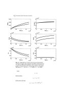
Electrical resistance of
electroformed nickel films shows a
unique
dependence on plating current
density (Figure 11). Films deposited at a low current density of 120 A/m2
show considerably lower residual resistance than high current density films
over the temperature range of
4
to
40
K
presumably due to codeposited
impurities in the low current density deposits
(44).
Small amounts of carbon in nickel and tin-lead electrodeposits can
noticeably influence tensile strength.
For example, increasing the carbon
content of a sulfamate nickel electrodeposit from 28 to 68 ppm increased
the tensile strength from
575
to
900
MPa, a noticeable increase in strength
with a few ppm
of
the impurity
(45).
Similarly, with tin-lead, increasing the
carbon content
of
the electrodeposit from 125 to
700
ppm increased the
tensile strength from
29
to
41 MPa (46). Carbon also increases the strength
Properties
127
Figure
10:
A
pictorial representation of the various types of inclusions in
electrodeposited films. From reference
42.
Reprinted
with
permission of
The Electrochemical SOC.
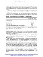
Table
4:
Influence of Current Density in Nickel Sulfamate Solution on
Impurity Content of Deposits (Ref
43).
am2)
(au-2,
c
H
Q
hl
s
54
5
70
10
44
8 30
323 30 80
3 28 8 8
538
50
60
4
32 8
6
128
Electrodeposition
Figure
11:
Resistance-temperature curves for electrodeposited nickel films
approximately
20
um thick. Adapted from reference
44.
of cast nickel and nickel-cobalt alloys but the effect isn’t as pronounced as
that for electrodeposits. For example, increasing the carbon from
20
to
810
ppm in cast nickel increases the flow stress from
190
to
250
MPa
(47).
Sulfur impurities can
be
harmful to nickel deposits which are
intended for structural or high temperature usage. For example, small
amounts
of
codeposited sulfur can noticeably influence notch sensitivity,
hardness and high temperature embrittlement. Charpy tests, which are
impact tests in which a center-notched specimen supported at
both
ends
as
a
simple
beam
is broken by the impact of a rigid, falling pendulum, showed
that deposits containing greater than
170
ppm
of
sulfur were highly notch
sensitive
(48,49).
Figure
12
shows
the
results of testing specimens of two
different thicknesses,
0.51
cm
(0.200
in), and
0.19
cm
(0.075
in).
An
increase
in
sulfur content is clearly shown to reduce the fracture resistance
of electroformed nickel. Whereas thicker specimens
(0.51
cm) displayed a
steady decrease
of
impact energy with sulfur content, thinner specimens
(0.19
cm) maintained roughly constant impact energy values up
to
160
ppm.
In
this
case, the thinner specimens were in a plane stress condition typified
by shear fractures and relative insensitivity
to
sulfur content.
In
contrast, the
Properties
129
Figure
12:
Influence
of
sulfur content on impact strength of electroformed
sulfamate nickel. The squares are
0.200
in. (0.51 cm) thick Ni and the
triangles are
0.075
in
(0.19
cm) thick Ni. Adapted from reference
48.
plane strain condition (no strain in the direction perpendicular
to
the applied
stress and crack length, reference
50)
existing in thicker specimens led to
higher triaxial tensile states and a significant sensitivity to sulfur content.
Sulfur also has a direct influence on the hardness of electrodeposited nickel
(Figure 13), therefore,
if
no other impurities are present in the deposit,
hardness can
be
used as an indicator of sulfur content
(48,49).
HIGH
TEMPERATURE EMBRITTLEMENT
OF
NICKEL AND
COPPER
Both nickel and copper electrodeposits undergo a ductile
to
brittle
transition at high temperature. With nickel, reduction in area drops from
greater than
90%
at ambient to around
25%
at a test temperature
of
500
C
(Figure
14,
ref 51). This effect occurs at a much lower temperature for
copper electrodeposits, e. g.,
100
to
300
C
depending on the conditions used
for electrodeposition (Figure
15,
ref
52).
130
Electrodeposition
Figure
13:
Influence of sulfur content on hardness of electroformed nickel.
Adapted from reference
49.
Properties
131
Figure
14:
Influence of temperature on reduction in area of
201
nickel and
electrodeposited sulfamate nickel. Adapted from reference
5
1.
Figure
15:
Influence
of
temperature on reduction in area for
OFE
(oxygen
free electronic) copper and electrodeposited copper. Adapted from reference
52.
132
Electrodeposition
Electrodeposited nickel is quite pure, especially when compared
with
201
wrought nickel which does not exhibit the ductile to brittle
transition (Table
5
and Figure
14).
The problem is that the electrodeposited
nickel is too pure. Embrittlement occurs because of formation of brittle
grain boundary films
of
nickel sulfide. Wrought
201
nickel doesn’t exhibit
the problem because it has sufficient manganese to preferentially combine
with the sulfur and prevent
it
from becoming an embrittling agent. By
codepositing a small amount
of
manganese with the nickel, the embrittling
effect can be minimized. The amount of manganese needed
to
prevent
embrittlement depends
on
the heat treatment temperature. The
Mn:S
ratio
varies from
1:l
for
200
C
treatments to
5:l
for
500
C
treatments
(51,53).
Embrittlement in electrodeposited copper
is
also probably due
to
grain boundary degradation stemming from the codeposition of impurities
during electroplating. It’s speculated that impurities modify the constitutive
behavior or produce grain boundary embrittlement that leads to plastic
instability and failure at small overall strains when compared with cast or
wrought material of comparable grain size
(54).
At
present the culprits have
not been identified but two likely candidates are sulfur and oxygen. For
example, cast high purity copper
(99.999+%)
is embrittled at high
temperature when the sulfur content is greater than
4
ppm
(55).
Oxygen in
cast copper has also been reported to cause embrittlement at high
temperaturcs, either under tensile or creep conditions
(56).
This
embrittlement is attributed
to
oxygen segregation to grain boundaries in the
copper which promotes grain boundary decohesion and enhances
intergranular failure. Both sulfur and oxygen can be present
as
impurities
in
electrodeposited copper.
OXYGEN
IN
CHROMIUM DEPOSITS
The relationship between the
internal
stress
in
chromium deposits
and their oxygen content is shown
in
Figure
16.
The broad band depicts the
scatter observed in many hundreds of experiments
(57).
These variations
are not unexpected because residual stress
in
any situation is related
to
the
well known cracking of chromium deposits. The changes were achieved by
changing the solution compositions at constant temperature
(86
C)
and
current density
(75
Ab2).
PHYSICALLY VAPOR DEPOSITED FILMS
With physically vapor deposited films, certain long term stability
problems may be due to gas incorporation during deposition
(58).
In
sputter
Properties
133
Table
5:
Composition of
201
Nickel and Electrodeposited Sulfamate
Nickel
201 Nickel Electrodeposited
Element
iQt2Lul
w1-
Copper
Iron
Manganese
Si1 ico n
Carbon
Cobalt
Hydrogen
Oxygen
Nitrogen
Sulfur
250 max
400 max
3500 max
3500 max
93
4700
2
17
6
12
<loo
<loo
<5
<
10
50
1000
8
20
6
10
'
Composition
of
the nickel sulfamate plating soloution was
80 g/l nickel (as nickel sulfamate),
<1
.O
g/l nickel chloride,
and 40 g/l boric acid. Wetting agent was used to reduce the
surface tension to 35-40 dyneskm. Current density was
268 Nm2; pH, 3.8; and temperature, 49'C. Anodes were sulfur
depolarized nickel.
deposition, up to
several
atomic percent
of
atoms
of
the sputtering gas can
be incorporated into the deposited film and this gas can precipitate into
bubbles or be released by heating
(59-64).
The incorporated gas can
increase the stress and raise the annealing temperature
of
sputter deposited
gold
films
(59).
Argon incorporation up to
1.5
at. % is possible in Tic
films and this causes compressive stresses of the order of
lo7
Pa. Such high
stresses give rise to lattice distortion which affects the dislocation properties
and
thus
the
hardness of
the
films
(60).
Similar effects are found
in
electron beam evaporated films where residual gases, often released by
heating during evaporation, are incorporated into the deposit and may cause
property changes
(64).
134
Electrodeposition
Figure
16:
Influence of oxygen on stress in chromium electrodeposits
produced at
86OC
and
75
A/dm2.
Adapted from reference
57.
Properties
135
REFERENCES
1.
2.
3.
4.
5.
6.
7.
8.
9.
10.
11.
12.
13.
W. H. Safranek,
The Properties
of
Electrodeposited Metals
and
Alloys,
American Elsevier Publishing Co.,
(1974)
W.H. Safranek,
The Properties
of
Electrodeposited Metals
and
Alloys,
Second Edition, American Electroplaters
&
Surface
Finishers
Soc.,
(1986)
D.S. Rickerby and S.J. Bull, "Engineering With Surface Coatings:
The Role
of
Coating Microstructure",
Surface
and
Coatings
Technology,
39/40, 315 (1989)
E.
Hornbogen, "On The Microstructure of Alloys",
Acta Metull.,
32, 615 (1984)
H.J. Read, "The Metallurgical
Aspects
of Hydrogen Embrittlement
in
Metal Finishing",
47th
Annual Technical Proceedings,
American
Electroplaters
SOC.,
110 (1960)
''Testing for Materials Selection",
Advanced Materials
&
Processes,
137,
No
6,
5
(June
1990)
D.
J.
Sandstrom, "Armor Anti-Armor Materials by Design",
Los
Alms Science,
17.36
(Summer
1989)
D.T. Game and G.M.H.
Lewis,
"Strain Hardening
of
High
Strength Steels",
Mater. Sci. Technol.,
1,
128 (1985)
D.T. Game and
U.
Ma, "Friction and Wear
of
Chromium
and
Nickel Coatings",
Wear
129,
123 (1989)
C.C.
Lo,
J.A. Augis and M.
R.
Pinnel, "Hardening Mechanisms of
Hard Gold",
J.
Appl.
Phys.
50,
6887 (1979)
D.E.
Sherlin and
L.K.
Bjelland, "Relationship
of
Comer Cracking
in
Multilayer Board Holes to Pyrophosphate Copper Plate",
Circuit
World,
4,
No
1, 22
(Oct
1977)
E.M. Hofer and H.E. Hintermann, "The Structure
of
Electrodeposited Copper Examined by X-ray Diffraction
Techniques",
J.
Electrochem.
SOC.,
1 12, 167 (1965)
R.E. Smallman and
K.H.
Westmacott, "Stacking Faults in
Face-Centered Cubic Metals and Alloys",
Phil.
Mag.,
2,669 (1957)
136
Electrodeposition
14.
15.
16.
17.
18.
19.
20.
21.
22.
23.
24.
25.
W.F. Schottky and M.B. Bever, "On the Excess Energy
of
Electrolytically Deposited Silver",
Acta Met.,
7, 199 (1959)
T.I.
Murphy, "The Structure and Properties of Electrodeposited
Copper Foil", Finishing Highlights,
71,
(Jan/Feb
1978)
H.R.
Johnson, J.W. Dini and
R. E.
Stoltz,
"The
Influence
of
Thickness, Temperature and Strain Rate
on
the Mechanical
Properties
of
Sulfamate Nickel Electrodeposits",
Plating
&
Surface
Finishing,
66, 57
(March
1979)
T.D. Dudderrar and F.B. Koch, "Mechanical Property
Measurements on Electrodeposited Metal Foils",
Properties
of
Electrodeposits, Their Measurement and Significance,
R.
Sard, H.
Leidhelser, Jr., and
F.
Ogburn, Editors, The Electrochemical
Society, Princeton, NJ
1975.
P. Vatakhov and
R.
Weil,
'The
Effects of Substrate Attachment
on
the Mechanical Properties of Electrodeposits",
PZating
and
Surface
Finishing
77, 58
(March
1990)
I.
Kim and
R.
Weil, "The Mechanical Properties of Monocrystalline
Nickel Electrodeposits",
Thin Solid Films,
169, 35 (1989)
S.
Mizumoto,
H.
Nawafune, M. Kawasaki,
A.
Kinoshita and K.
Araki,
"Mechanical Properties of Copper Deposits from Electroless
Plating Baths Containing Glycine",
Plating
&
Surface Finishing
73,
48
(Dec
1986)
M. Paunovic, "Significance of Tensile Testing Copper Deposits",
Plating
&
Surface Finishing,
70, 16
(Nov
1983)
M.
Parente and R. Weil,
Plating and Surface Finishing,
71, 114
(May
1984)
I.
Kim and
R.
Weil, "Thickness Effects on the Mechanical
Properties of Electrodeposits",
Proc. SURIFIN
88,
AESF,
Orlando,
Fl.
1988
N.J. Petch, 'The Cleavage Strength of Polycrystals",
Journal of
the
Iron and Steel Institute,
174,
25
(1953)
R.
Walker and R.C. BeM, "Microhardness. Grain Size and
Topography
of
Copper Electrodeposits",
Plating,
58,476 (1971)
Properties
137
26.
27.
28.
29.
30.
31.
32.
33.
34.
35.
36.
37.
38.
H. McArthur,
Corrosion Prediction
and
Prevention in Motor
Vehicles,
Ellis Horwood Ltd., England
(1988)
V.M. Kozlov, E.A. Mamontov and Yu. N. Petrov.,
Fiz. Metal. i
MetaJloved,
26 (3). 564 (1968)
G.D. Hughes,
S.D.
Smith,
C.S. Pande, H.R. Johnson and R.W.
Armstrong, "Hall-Petch Strengthening for the Microhardness of
Twelve Nanometer Grain Diameter Electrodeposited Nickel",
Scripra Metallurgica,
20, 93 (1986)
A.W. Thompson and H.J. Saxton, "Structure, Strength and Fracture
of Electrodeposited Nickel and Ni-Co Alloys",
Metallurgical
Transactions,
4,
1599 (1973)
C.P. Brittain, R.W. Armstrong and G.C.
Smith,
"Hall-Petch
Dependence
for
Ultrafine Grain Size Electrodeposited
Chromium",
Scripta
Metallurgica,
19,
89 (1985)
H.W. Hayden, R.C. Gibson, and J.H. Brophy, "Superplastic
Metals",
Scienfific American,
220,
28
(March
1969)
A. Goldberg, "Materials Engineering",
Energy
and
Technology
Review,
Lawrence Livermore National Laboratory,
3
(March
1987)
N.P.
Barykin, R.Z. Valiyev, O.A. Kaybyshev and F.A. Sadykov,
"Superplastic Behavior
of
an Electrodeposited Coating of Eutectic
Alloy Cd-Zn",
Phys. Met. MetaJJogr.
(USSR),
63 (2), 157 (1987)
R.J. Walter, "Tensile Properties of Electrodeposited Nickel-Cobalt",
Plating
&
Surface Finishing,
73.48
(Oct
1986)
R.J. Walter and H.E. Marker, "Superplastic Alloys Formed by
Electrodeposition",
US
Patent
4,613,388,
Sept
1986
P.J. Martin and W.A. Backofen, "Superplasticity in Electroplated
Composites of Lead and
Tin",
Transactions
of
the
ASM,
60,
352,
1967
M.M.I. Ahmed and T.G. Langdon, "Exceptional Ductility in
the
Superplastic
Pb62
Pct Sn Eutectic",
Metallurgical Transactions A,
8A,
1832, (1977)
P.S.
Venkatesan and G.L. Schmehl, "Superplasticity in Metals",
The
Western Electric Engineer,
Vol
XV,
2
(Jan
1971)
Electrodeposition
138
39.
40.
41.
42.
43.
44.
45.
46.
47.
48.
49.
50.
G.K. Maltseva and A.V. Belyanushkin,
Izv.
AM.
Nauk
SSSR,
Met.
5,
134 (1988)
D.
S.
Lashmore, R. Oberle and M.P. Dariel, "Electrodeposition of
Artificially Layered Materials",
Proc.
AESF
Third International
Pulse Plating Symposium,
American Electroplaters
&
Surface
Finishers
Soc.,
(&t
1986)
D. Tench
and
J.
White,
"Enhanced Tensile Strength for
Electrodeposited Nickel-Copper Multilayer Composites",
Metallurgical Transactions
A,
15A,
2039 (1984)
S.
Nakahara, "Direct Observations of Inclusions in Electrodeposited
Films by Transmission Electron Microscopy",
J.
Electrochem.
SOC.,
129,201C (1982)
J.W. Dini and H.R. Johnson, "The Influence of Nickel Sulfamate
Operating Parameters on the Impurity Content and Properties of
Electrodeposits",
Thin Solid Films,
54,
183 (1978)
O.B.
Verbeke,
J.
Spinnewin and H. Strauven, "Electroformed
Nickel for Thermometry
and
Heating",
Rev.
Sci.
Instrum.,
58
(4),
654
(April
1987)
J.W. Dini and H.R. Johnson, "Influence of Carbon on the Properties
of Sulfamate Nickel Electrodeposits",
Surface Technology,
4,
217
(
1976)
R.R. Vandervoort, E.L. Raymond, H.J. Wiesner and W.
P.
Frey,
"Strengthening of Electrodeposited Lead and Lead Alloys,
II-
Mechanical Properties",
Plating
57,
362 (1970)
D.E. Sonon and G.V. Smith, "Effect of Grain Size and Temperature
on
the
Strengthening of Nickel and
a
Nickel-Cobalt Alloy by
Carbon",
Trans. Metallurgical
SOC.
AIME,
242, 1527 (1968)
J.W. Dini, H.R. Johnson and H.J. Saxton, "Influence of Sulfur
Content on the Impact Strength of Electroformed Nickel",
Electrodeposition and Surface Treatment,
2, 165 (1973t74)
J.W.
Dini,
H.R. Johnson and H.J. Saxton, "Influence of
S
on the
hoperties of Electrodeposited Ni",
J.
Vac. Sci. Technol.,
12,
No
4,
766
(July/August
1975)
J.P. Chubb. "Fracture Mechanics-A Break for the Metallurgist?",
Metallurgia,
46,493
(August
1979)
Properties
139
51.
52.
53.
54.
55.
56.
57.
58.
59.
60.
61.
62.
63.
J.W. Dini, H.R. Johnson and L.A. West, "On the High Temperature
Ductility Properties
of
Electrodeposited Sulfamate Nickel",
Plating
&
Surface Finishing,
65, 36
(Feb
1978)
D.H. Lassila, "Material Characteristics Related to the Fracture and
Particulation of Electrodeposited Copper Shaped Charge Jets",
Lawrence Livermore National Laboratory
UCRL-102520,
April
1990
WR. Wearmouth and K.C. Belt, "Electroforming With Heat
Resistant
Sulfur
Hardened Nickel",
Plating
&
Surface Finishing,
66, 53
(Oct.
1979)
J.W. Dini and W.H. Gourdin, "Evaluation
of
Electroformed Copper
for
Shaped Charge Applications".
Plating
&
Surface Finishing,
77,
54
(August
1990)
M. Myers and E.A. Blythe, "Effects of Oxygen,
Sulphur,
and
Porosity
on
Mechanical Properties
of
High-Purity Copper at
95OC",
Metals Technology,
8, 165
(May
1981)
T.G. Nieh and W.D. Nix, "Embrittlement
of
Copper Due to
Segregation
of
Oxygen
to
Grain Boundaries",
Met. Trans.
A,
12A,
893 (1981)
L.H. Esmore, "The Electrodeposition
of
High Purity Chromium",
Trans. Institute
of
Metal Finishing,
57, 57 (1979)
D.M. Mattox,
"Thin
Film Metallization
of
Oxides In
Microelectronics",
Thin Solid Films,
18, 173 (1973)
H.F. Winters and E. Kay, "Gas Incorporation Into Sputtered Films",
J.
Appl. Phys.,
38, 3928 (1967)
A. Pan and J.E. Greene, "Residual Compressive Stress
in
Sputter
Deposited Tic Films on Steel Substrates",
Thin Solid Films,
78,25
(1981)
D.M. Mattox and G.J. Kominiak, "Incorporation
of
Helium
in
Deposited Gold Films",
J.
Vac. Sci. Technol.,
8,
194
(1971)
A.J.
Markworth, "Growth Kinetics of Inert-Gas Bubbles
in
Polycrystalline Solids",
J.
Appl. Phys.,
43, 2047 (1972)
E.V.
Kornelsen,
"The
Interaction
of
Injected Helium With Lattice
Defects in a Tungsten Crystal",
Radiation Eflects,
13, 227 (1972)
140
Electrodeposition
64.
S.K.
Dey
and
A.M.
Dighe,
"A
Suitable Deflection Electrode
Geometry
for
Removal
of
Ions
Inside
Deposition
Chambers",
Solid
Stare
Technology,
15, 51
(Ckt
1971)
STRUCTURE
INTRODUCTION
Almost all plated metals are crystalline, which means that the atoms are
arranged on a regular three dimensional pattern called a lattice
(1).
The
three most important lattices are face centered cubic (fcc), body centered
cubic (bcc) and hexagonal close packed (hcp), all shown in Figure
1.
Face
centered cubic packing of spheres often seen in
fruit
stands
or
in piles of
cannonballs at war memorials,
is
the densest packing of spheres in three
dimensional space
(2,3,4).
Table
1
lists the lattices for the commonly plated
metals. However, it’s important to note that incorporation of foreign species
can modify the structure of deposited metals. For example, a structural
transition from unstable hexagonal chromium hydride
to
body
centered
cubic chromium during
or
soon after plating accounts for the cracking
observed in chromium deposits. This decomposition involves a volume
shrinkage of greater
than
15
percent
(5).
More discussion on microstructur-
al transformations
of
deposits will be presented later in this chapter.
Additional topics that will be covered include texture and fractals.
STRUCTURE OF ELECTRODEPOSITED AND ELECTROLESS
COATINGS
The properties of all materials are determined by their structure.
Even minor structural differences often have profound effects on the
properties of electrodeposited metals
(6).
Four typical structures encoun-
tered with electrodeposited metals include;
1)
columnar,
2)
fibrous,
3)
fine-grained, and
4)
banded
(7).
Cross
sections showing each type are
141
142
Electrodeposition
Table
1
-
Lattice Structure
of
Commonly
Plated Metals
Face centered Hexagonal Body centered
m
!2lQ%w&m
Tetraaonal
Ag
cd
cr
Sn
AI
co
Fe
Au
zn
cu
Ni
Pb
Pd
Pt
Rh
Figure
1:
Unit cells of the three most important lattices.
included in Figures
2
to
6.
Columnar structures (Figure
2)
are characteristic
of
deposits from
simple ion acidic solutions containing no addition agents, e.g., copper, zinc,
or
tin from sulfate or fluoborate solutions, operated at elevated temperature
or
low
current density. Deposits
of
this
type
usually exhibit lower strength
and hardness
than
other structures but high ductility.
Structure
143
Figure
2:
Large, Columnar Grains-cross section of a deposit produced in
a citrate based acid gold solution
(200
x).
Fibrous (acicular) structures, which represent a refinement
of
columnar structure, are shown in Figure
3.
This type of structure is
obtained because some factors in the deposition process such as the
presence of addition agents, or use of low temperature and high current
density in copper sulfate solutions, have favored the formation of new
nuclei rather than growth of existing grains. The finer grain size may
be
the
result of interference
of
crystal growth by codeposited metal hydroxide or
hydrogen
(7).
Properties
of
fibrous deposits are intermediate between
columnar and fine-grained deposits.
Fine-grained structures (Figure
4)
are usually obtained from
complex ion solutions such as cyanide
or
with certain addition agents.
These deposits are less pure, less dense and exhibit higher electrical
resistivities due to the presence of codeposited foreign material. Deposits
from simple ion acidic solutions, such as copper or nickel from sulfate
solutions, develop this structure if operating conditions are more extreme
144
Electrodeposition
Figure
3:
Fibrous (Acicular) Structure-cross section
of
a deposit produced
in a nickel sulfamate solution
(200
x).
Figure
4:
Fine Grained Suucture-cross section
of
a deposit produced in
a
copper cyanide solution
(200
x).
Structure
145
than those that produce deposits of
the
type shown in Figure
3.
For
example, a very high current density, a high pH (in the case
of
a nickel
solution) resulting in codeposited hydrated oxides,
or
certain addition agents
may cause the formation of this type of structure
(7).
The grain sizes in
deposits of this
type
are
of
the order
of
lo-’
to cm. These deposits are
usually relatively hard, strong and brittle but
it
is important to realize that
some fine-grained structures can be quite ductile
(30%
elongation) and the
grain size
so
small that it is virtually unresolvable, as shown in Figure
5
(8).
Laminar
(or
banded) structures are shown in Figure
6.
The grains
within
the
lamellae are extremely small. These structures are characteristic
of
bright deposits resulting from addition agents such as sulfur containing
organic compounds which result in small amounts of
S
and
C
in the deposit.
A
number
of
alloy deposits such as gold-copper, cobalt-phosphorus, cobalt
-tungsten, and nickel-phosphorus (electroless and electrodeposited) exhibit
this
structure. These deposits usually have high strength and hardness but
low ductility. Similar laminations can
be
found in deposits produced in
solutions operated with either periodic reverse current
or
pulse plating.
Figure
5:
Very Fine Grained Structure-cross
section of a deposit
produced in a copper sulfate solution containing proprietary additives
(500
XI.
146
Electrodeposition
Figure
6:
Laminated
(or
Banded) Struciure-cross section of a gold-copper
deposit
(250
x).
The crystal structure resulting
from
an electrodeposition process is
strongly dependent on the relative rates of formation of crystal nuclei and
the growth of existing crystals
(9,lO).
Finer-grained deposits are the result
of conditions that favor crystal nuclei formation while larger crystals are
obtained in those cases that favor growth of existing crystals. Generally, a
decreasing crystal size is the result
of
factors which increase the cathode
polarization
(9.1
0).
From the electroplaters’ viewpoint,
it
would be nice
to
have some
three
dimensional picture that would show the influence of operating
conditions on structure. However, since plating processes have numerous
variables that influence structure, e.g., metal ion concentration, addition
agents, current density, temperature, agitation, and polarization, a plot such
as that shown in Figures
8
and
9
for
physically vapor deposited films cannot
be
produced. However, Figure
7
does pictorially show
how
individual
plating variables influence grain size of electrodeposits
(1
1).
Structure 147
Figure
7:
Relation of structure
of
electrodeposits
to
operating conditions
of solutions. From reference 11.
Figure
8:
Structural zones in PVD films. From Movchan and Demchishin,
reference 13. Reprinted with permission of Noyes Publications.
148
Electrodeposition
Figure
9:
Structural zones in PVD films. From Thornton, references
14,
15.
Reprinted with permission of Noyes Publications.
STRUCTURE
OF
PHYSICALLY VAPOR DEPOSITED COATINGS
With physically vapor deposited (PVD) coatings there have been
three
distinct steps taken in the classification of thin film morphology (12).
Movchan and Demchishin (1
3)
were the first to classify thin films using a
structure zone model
(SZM).
They observed that regardless of the thin film
material, its morphological structure is related to a normalized,
or
reduced,
temperature TDm, where
T
is the actual film temperature during deposition,
and Tm is its melting point, both in
K
(12). They found that by increasing
the deposition temperature, they could obtain at least three qualitatively
distinct structure zones (Figure
8).
Zone 1 in their classification consists of
tapered columns with domed tops and is in a region of low adatom
mobility.
In
zone
2,
the structure is of a straight columnar nature and has
a smooth surface morphology. For zone
3
the physical structure resembles
equiaxed crystallites, much the same as those found in recrystallized metals.
Unlike Movchan and Demchishin
(1
3)
who prepared their films by
electron beam evaporation, Thornton (14,15) used magnetron sputtering and
introduced
a
new parameter, the sputtering gas pressure. He showed that
both
TDm
and
the
sputtering gas pressure have an identifiable and
significant effect on thin film growth
(12).
Thornton’s model includes a
fourth transition zone, called zone T, between zones 1 and 2 (Figure
9). In
this zone the films have a smoother surface morphology and are denser than
films from the surrounding zones (12).
Structure
149
Recently, Messier and colleagues, have shown that the physical
structure of thin films changes as a function of thickness
(12.16-19).
A
distribution
of
sizes from the smallest clustered units (pm-sized)
to
the
largest, dominant sizes perceived, typically p-size units in
SEM
micro-
graphs, is the resulting structural heterogeneity
(16).
Thornton’s model is
essentially retained in this new SZM which includes the similarity in
morphology of various levels of magnification as well as the evolutionary
growth
of
morphology (17).
A
revised SZM model
for
zone
1
structures is
shown in Figure 10, wherein all the distinct levels
of
physical structure
column/void sizes are considered and assigned subzones
lA,
lB,
lC,
1D
and 1E
(17).
The smallest size level
(1-3
pm) is represented by zone
1A
and the largest by zone
1E
(300
pm
column sizes). Larger sizes can
be
assigned designations of lF, lG, etc. This structure is not unique
to
the
deposition technique but has been found in
all
vapor deposited films, as
well as electrodeposited films (12,18). This universality in the physical
structure
of
a variety
of
materials and self-similarity in structural evolution
indicates a common origin
of
thin film growth and a possible fractal
description (12,16,18,19). Fractals are discussed later in this chapter.
Figure
10:
Revised structure zone model
for
films. From Messier, Giri
and Roy, reference
17.
Reprinted with permission of the American Vacuum
Society.
150
Electrodeposition
INF'LUENCE
OF
SUBSTRATE
The structure of most electrodeposits is determined by epitaxial and
pseudomorphic
growth
onto a substrate and by the conditions prevailing
during deposition. Typically, a deposited metal will
try
to copy the
structure of the substrate and
this
involves epitaxy, which occurs when
definite crystal planes and directions are parallel in the deposit and
substrate, respectively (1,20). Epitaxy is the orderly relation between the
atomic lattices of substrate and deposit at the interface, and is possible
if
the
atomic arrangement in a certain crystal direction of the deposit matches that
in
the substrate. Another term, pseudomorphism, refers to the continuing
of
grain boundaries and microgeometrical features of the cathode substrate
into the overlying deposit.
A
deposit stressed to fit on the substrate is said
to
be
pseudomorphic
(20).
Pseudomorphism persists longer than epitaxy.
The structure of a deposit and its properties and adhesion can be
noticeably influenced by the substrate upon which it is plated. Figure 11
shows cross sections of copper electrodeposited on cast copper
(9).
If the
substrate was cleaned but not pickled prior to plating, the structure of the
plated deposit was quite different (fibrous) compared to that of the cast
copper (coarse grained), Figure
lla.
However, use of pickling after
cleaning resulted in a structure wherein the copper crystals were continua-
tions of the crystals in the copper basis metal (Figure
l
lb). Such reproduc-
tions of the basis metal structure may occur even with dissimilar metals that
may vary appreciably in lattice structure and spacing (21).
The effect
of
the type
of
substrate on the properties of nickel
electrodeposited on as-rolled and on annealed, cube-textured copper sheet
is shown in Table
2.
The influence of the small grain size induced in the
deposits plated on the as-rolled sheet is apparent in the higher strength and
ductility, compared with the deposit plated on the annealed, cube textured
sheet which was coarse-grained (22)
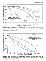
Figures 12 and 13 show the influence of substrate on elongation of
copper deposited from an acid sulfate solution (23). With 304 stainless
steel
as
the substrate, the elongation of the copper was highly irreproducible
and drifted alternately between high and
low
values (Figure 12). Accept-
ably reproducible results were obtained
with
a much more corrosion
resistant substrate, Inconel
600
(Figure 13).
PHASE TRANSFORMATIONS
A
phase transformation is a change in the number or nature of
phases as a result of some variation in the externally imposed constraints
such as the temperature, pressure, or magnetic field.
As
will
be
shown in