SMT Soldering Handbook surface mount technology 2nd phần 8 pptx
Bạn đang xem bản rút gọn của tài liệu. Xem và tải ngay bản đầy đủ của tài liệu tại đây (2.74 MB, 42 trang )
job:LAY07 page:4 colour:1 black–text
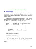
Figure 7.1
Angular accuracy of placement
Positional accuracy
With fine-pitch lead spacing, the width of the footprints is half their distance.
Fine-pitch below 0.5 mm/20 mil and ultrafine-pitch with 0.25 mm/10 mil spacing
have become real demands. This means footprints 0.125 mm/5 mil wide, and lateral
placement accuracies of ±0.06 mm/2.5 mil. Pick-and-place equipment with a
placement accuracy of ±0.05 mm/2 mil, and a repeatability of ±0.02 mm/0.8 mil is
commercially available.
Angular accuracy of placement also matters. With a QFP of dimensions 25 mm/
1in; 25 mm/1 in, an angular twist of 1° means a lateral displacement of 0.22 mm/
8 mil at every corner. As a result, with a fine-pitch layout, about half the legs would
sit on the wrong footprint (Figure 7.1). Therefore, with large fine-pitch compo-
nents, angular placement accuracy has to move into the ±0.1° bracket.
Because BGAs and flip-chips are able to correct even massive misplacement by
self-alignment as soon as the solder melts (see section 2.2), the accuracy of their
placement is less critical.
Component identity and functionality checks
The number of placement errors is a measure of the reliability of a placement
system. Until not so long ago, wrong-value chips and melfs in blistertape or bulk
packages contributed significantly to manufacturing reject rates. Smart placement
systems, which detect and correct such errors during placement ‘on-the-fly’
brought a drastic improvement and have become a common feature with most
automatic placement machines.
252 Component placement
job:LAY07 page:5 colour:1 black–text
7.3 Placement options
A user must decide between two strategies of component placement: on the one
side are the manual and semi-automatic manual methods, on the other the fully
automatic ones, which also fall into two categories, the sequential and the simulta-
neous systems. The choice between them depends on several factors:
1. A newcomer to SMD technology who operates on a small-to-medium scale
will tend to opt for a manual or semi-automatic system, unless he is part of an
organization where in-house know-how and technical assistance with fully
automatic systems are available.
2. The type of product and the volume of production are crucial factors. If there
are no more than about 50, at most 100 components, on a board, however
complex their function and the layout, and if the number of boards does not
exceed a few hundred per working day, a manual, probably semi-automatic
placement system may well be the best choice.
As the number of boards to be processed per day rises, the cost effectiveness of
purely manual placement soon drops. Semi-automatic placement reaches its maxi-
mum cost efficiency in the middle range of production volume, particularly where
full-time working is not always guaranteed.
A further factor which affects the choice of system is the product mix: if the
boards are all customer-specific boards, each with a short or unpredictable length of
run, and if production must be flexible and capable of coping with frequent
changes, semi-automatic manual placement may be best. It is worth noting, though,
that recent years have seen the arrival of several fully automatic pick-and-place
machines of great flexibility, with facilities for a rapid change-over from one
working program to another.
In the last resort, the size of the necessary investment must be decisive. Naturally,
manual and semi-automatic equipment is cheaper, and writing it off is less of a
problem when faced with a fluctuating and highly differentiated demand. On the
other hand, where one or a number of soldering lines must be fed with assembled
boards, without the risk of costly interruptions, one or more fully automatic
pick-and-place installations are the best, if not the only choice.
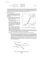
7.3.1 Fully manual placement
Like every placement system, placing SMDs by hand involves two steps: finding and
fetching the component, and then putting it down on its footprints, having rotated
it into its correct orientation (Figure 7.2). With boards to be wavesoldered,
placement is preceded by putting down the spots of adhesive with a handheld
syringe or by hand stencilling. The footprints of boards to be reflowsoldered are
provided with solder paste, again from a syringe, a metering dispenser, or by manual
stencilling.
As with all manually operated processes, good ergonomic design of the work
place is the precondition to get the best possible results with a minimum of errors.
Even so, manual placement without any additional aids like assigning to each type of
Component placement 253
job:LAY07 page:6 colour:1 black–text
Figure 7.2
The basic tasks of manual placement
component its proper set of footprints, needs good housekeeping and unremitting
concentration. It should be practised only for assembling small numbers of proto-
type boards, or very simple assemblies with few types of components.
Even with entirely manual placement, no component should ever be touched
with bare fingers. As has been said several times already, however clean fingers are,
they will transfer fatty acids and salts to the components and their soldering surfaces.
This affects their solderability, especially if adhesive joints must be cured before
soldering. The curing heat greatly intensifies the damaging effect of any surface
contamination on a soldering surface.
Tweezers can be used for handling the components, but a vacuum pipette with a
finger-actuated rotatable head is much more convenient. The pipette may be
handheld, or mounted on a gantry which is operated by a ‘joystick’. With both, the
accuracy of placement depends on the normally very high degree of coordination
between the human eye and the human hand. Most operators, with some training,
have no problem in putting down components on fine-pitch footprints without
smudging the solder paste. It may be worth remarking here that, so far, no vendor
seems to have found it worth his while to provide manual placement equipment
which can be converted for left-handed operators.
With manual placement, there are three kinds of possible errors: picking the
wrong component, putting it in the wrong place and, with active components,
placing it the wrong way round. Every manual placement system, however well
conceived, which uses a bulk feed system of loose melfs or chips contains one
further, and dangerous, source of placement error: one or more stray components
may have found their way into the wrong compartment of a carousel or feeder box.
If such an error is noticed, or maybe only suspected, it may be simpler and cheaper
to discard the contents of the whole compartment than to try to find the rogue
components amongst several hundred correct ones.
It is important to allow the operator regular intervals of rest, at least five to ten
minutes every hour. It has been found that, depending on the complexity of the
board and the number of component types, the error rate rises rapidly with less than
that amount of rest time. With ten to twenty components per board and not more
254 Component placement
job:LAY07 page:7 colour:1 black–text
than ten different types of components, placement rates of up to 500 or 600
components per hour can be realized with purely manual placing. This can drop to
300/hour with more complex boards.
Components may be picked from a turntable (carousel) which is subdivided into
a number of compartments holding loose components, from a row of horizontal
feeders, which present the components from the open ends of blistertapes, from
stick magazines or waffle trays.
With purely manual placement, the error rate may drop below 0.1%, i.e.
:1000 ppm. But errors there will be, and in order to avoid expensive rework it is
strongly advisable to inspect every board for correct placement before soldering it.
Corrections are made by lifting off the offending component. Melfs and chips,
unless valuable, are best discarded. SOs and gullwing-legged components can be
re-used, after the legs have been cleaned with isopropanol. The footprints are wiped
clean of solder paste with a small piece of cotton or linen soaked with isopropanol.
Dots of adhesive are best left alone, lest they be smeared over a footprint, which will
become unsolderable. Adhesive vendors may be able to recommend or supply a
suitable solvent to clear off an adhesive spot. The place having been cleaned up,
fresh solder paste (or adhesive) is put down and the component is replaced.
7.3.2 Semi-automatic placement
Semi-automatic placement machines take over some of the tasks of manual place-
ment. These are principally those where human error could creep in, such as
picking the right component and putting it in its correct place. Moving the
components from their feeders to their footprints, and putting them down with the
necessary precision, is still left to the sensory and muscular feedback system between
the human eye and hand, a system which can be replicated by electromechanical
and opto-electronic means only at great expense.
All semi-automatic manual placement machines are linked with a computer
system, which can be either integral to the machine or operated by a separate PC.
Such a system can be programmed to indicate by an LED or a spot of light the feeder
from which the next component must be fetched. At the same time, the place
where it has to be put down is illuminated by a beam of light, or indicated in some
other way.
These functions can be refined and added to. Some semi-automatic placement
machines make only the correct feeder accessible, while the others are covered.
Feeders are mechanized to automatically present the next component after the
precedingonehas beencollected. Thevacuumpipette whichhandles thecomponent
can be mounted on a traversing mechanism which first guides it to the correct feeder,
and then to the correct location above its placement position. The operator then
lowers the pipette and guides it to its exact position. As the component touches
down, the vacuum in the pipette may be released automatically. Finally, the
controlling computer can be programmed to work out the most economical
placementsequenceto savetime-wastingmovements. Depending on the complexity
of the board and the mix of components, the capacity of semi-automatic placement
systems with full computer support can rise to about 900 components per hour.
Component placement 255
job:LAY07 page:8 colour:1 black–text
Figure 7.3
Sequential placement
7.3.3 Fully automatic sequential systems
General features
The term ‘sequential’ means that, as with the manual systems, the machine always
places one component at a time (Figure 7.3). Apart from that, a fully automatic
sequential placement system is like a semi-automatic manual system, with the
human element replaced by opto-electronic and electromechanical means. Taking
out the human element has several consequences:
1. Fully automatic equipment is more expensive, by one or more orders of
magnitude.
2. Fully automated sequential placement is faster, with a capacity of up to 60 000
components per hour.
3. The high accuracy of placement demands a robust and stable platform on which
the moving parts are mounted. This in turn means a design based on the
technology of a precision machine tool rather than of a mechanical plotter.
Flexibility
With most users of pick-and-place equipment, flexibility of the system is a crucial
requirement in order to reduce down-time of the expensive equipment to a
minimum. In this context, flexibility means the ease and speed with which a
machine can be switched from one type of board to another. Such a change-over
involves changing the array of feeders and the pick-and-place sequence. The latter
needs little time if the operating software already exists. If it does not, it can often be
created while the machine is still busy placing components on another board.
Assembling the array of feeders and loading them with the required tapes and
magazines takes more time. Many state-of-the-art machines have mobile feeder
arrays which can be assembled away from the machine. An array can be fully loaded
with the tapes and magazines for the next run while the machine is still busy on the
preceding one. For the change-over, feeder arrays can be quickly exchanged against
one another. Working out the best sequence of components in a feeder array,
256 Component placement
job:LAY07 page:9 colour:1 black–text
together with the most economical pick-and-place sequence, is a matter of software
and programming.
Additional functions
Apart from picking and placing components, most automatic pick-and-place
machines can put down single drops of adhesive for SMDs which are to be
wavesoldered. When placing BGAs or flip-chips on ‘bare’ footprints, which have
not been provided with a deposit of solder paste, several placement machines have
the facility to give the component a shallow dip in a tray of no-clean flux between
pick-up and placement.
‘Smart’ machines
Smart machines observe and react to circumstances, and detect errors and take the
appropriate action. In the context of component placement, this includes the
following:
E Feeder units identify the tapes or magazines loaded into them, and in the case of
an error give a signal or prevent operation until the mistake is rectified.
E Placement heads identify the components they have picked up, and check some
of their basic functions (‘in-flight testing’). Multilead components are checked
for the coplanarity of the lead ends.
E Vision centring systems align fine-pitch components with their footprints
before setting them down.
Grouping of placement units
Placement lines can be assembled from individual automatic placement units, which
are linked together and operated as a CIM system. This makes it possible to multiply
the capacity of the placement section while still maintaining its flexibility to respond
quickly to changing production requirements.
7.3.4 Simultaneous placement systems
Some types of electronic product like domestic audio and video equipment involve
long runs of similar boards which are not particularly complex but which are
produced in large volume. These boards are soldered on high-capacity lines, which
may be wave machines or reflow ovens. They in turn must be fed by placement
equipment of equally high output.
For this task, simultaneous placement systems are better suited. As the name
implies, a number of components are picked and placed at the same time at every
working stroke of the machine (Figure 7.4). A number of placement arms, each of
which can choose between several feeders, pick up components simultaneously.
The length of the stroke of each arm determines where the component comes
Component placement 257
job:LAY07 page:10 colour:1 black–text
Figure 7.4
Simultaneous placement
down. If the boards are to be wavesoldered, a dot of adhesive is placed on the
underside of each component as it moves forward to be placed.
7.4 The practice of automatic component placement
7.4.1 The range of choice
One of the driving forces behind the development of automatic placement equip-
ment is the evolution of the SMDs themselves. In some respects this seems to have
reached a plateau, at least a temporary one: the miniaturization of melfs and chips
(‘birdseed’ in the language of component users) has probably stopped with compo-
nents 1 mm/40 mil wide and 2 mm/80 mil long. The size of multilead components
may have reached a temporary limit with 55 mm/2.2 in square, which with a
0.5 mm/20 mil pitch gives a leadcount of about 400. The makers of automatic
placement equipment have responded, many of them in collaboration with their
customers. The advent of flip-chips and BGAs posed no fresh problems; if anything,
the accuracy of placement is less critical because of the capacity of these components
for self-alignment, after the solder has melted (see Section 3.6.3).
An essential requirement will all placement machines is a robust construction,
resembling that of a machinetool rather than of a piece of office equipment, which
needs frequent attention. The importance of a high placement speed depends very
much on whether the machine is part of a high-output assembly line, soldering a
limited number of types of board, or whether the user solders comparatively shorter
runs of a larger variety of boards, as would be the case with a contract assembler for
example. Common needs of most users are ease and storability of programming, a
wide range of components which the machine can handle, and speed of change-
over from one placement program to another.
A recent survey lists 24 vendors in the USA, Europe, and Japan. The functional
capabilities of the equipment which they offer is classified in Table 7.2.
Choosing a placement system poses formidable problems. In terms of size of
investment, it may well equal if not exceed the cost of the soldering equipment.
258 Component placement
job:LAY07 page:11 colour:1 black–text
Table 7.2 Functional capabilities of commercially available automatic SMD placement equipment
(1996)
Capability Percentage of available
equipment offering
the capability
Capable of in-line integration 100%
Placing 910 000 SMDs/hour 80%
Machine vision to assist placement 95%
Handling SMDs with :0.4 mm/16 mil pitch 75%
Handling TABs and BGAs 60%
There is no single machine which is simultaneously the fastest, the most flexible, the
most accurate and the cheapest. All attributes must be traded off against one another.
However, most of today’s automatic placement machines are conceived as
modules which can be added to one another into an integrated line, and this makes
the choice easier: a newcomer to automatic placement can start with a unit of
comparatively modest capability and cost, without pre-empting his later options for
expansion.
7.4.2 Classes of placement machines
Entry-level and mid-range machines
A buyers’ guide, already mentioned above, lists 66 different models of placement
machines, catering for a wide range of requirements. At what is sometimes termed
the ‘entry-level’ and the ‘mid-range’ of placement machines, up to 100 feeder
stations are provided with a changeable mix of bulk-feeders, feeder tape, and
stick-tray and waffle-tray magazines. With many machines, sets of feeder stations are
mounted on individual, interchangeable trolleys which can be quickly detached
from, or linked to, the machine to increase flexibility and speed up the change-over
from one type of board to another. The feeder stations on each trolley are assembled
according to a computer-generated sequence to suit a given type of board. This
enables the machine to switch from one type of board to another very quickly.
The single placement heads collect, centre, rotate and put down single compo-
nents in sequence. Most of these single-head machines have a maximum theoretical
placement rate of 4000 components per hour. In practice, the necessary allowance
for travel time and stop-and-start movements reduces the practically achievable rate
of placement to about 2400 components per hour.
This type of operation is suitable for placing melfs, chips and SO components
with standard pitches from 1.25 mm/50 mil down to 0.65 mm/26 mil. For placing
components with finer pitch, machines are either equipped, or can be retrofitted,
with opto-electronic placement aids. Facilities for in-flight verification of compo-
nent identity and functional integrity can also be provided.
Component placement 259
job:LAY07 page:12 colour:1 black–text
With single-head placers, putting down drops of adhesive on boards destined for
wavesoldering would require a second placement station. For this reason, it is
economical to feed this type of machine with boards to which the adhesive has been
pre-applied by one of the methods described in Section 4.8.3.
Fine-pitch placement machines
Next in line are fine-pitch placement machines, which can cope with placement
accuracies up to 0.4 mm/15 mil and component sizes up to 55 mm/2 in square,
which means maximum xy and rotational accuracies. Such machines are fully
equipped with opto-electronic sighting, verification of the coplanarity of compo-
nent legs, and automatic adjustment of placement pressure so as not to smudge or
squeeze out the paste printdown on the narrow footprints. With a single head, the
maximum output is as above.
High-speed ‘chip-shooters’
The next step in sophistication are the high-speed ‘chip-shooters’. Different equip-
ment makers have chosen different paths to this end. With one system, for example,
the placement head takes the form of a rotating disc (revolver head) with twelve
circumferential stations, each of which grips one component. With a two-head
machine, one disc loads up while the second one puts down its load of components
on the board. Instead of the second revolver disc, a single placement head for very
large multilead components can be substituted. A further head for pre-placing
metered amounts of adhesive can also be fitted. The placement rate of such
machines is quoted at 13 000 components per hour.
Very high speed placement machines
Three machines listed in the already mentioned guide have capacities of between
20 000–30 000 components/hour, two can place up to 40 000/hour, and one
(Philips) up to 60 000/hour. The latter operates with six XY heads, each of them
populating separate areas of the same board. Most of the other high-speed placers
use turret systems for handling the components. One machine is capable of placing
components simultaneously on both sides of a board.
7.5 Reference
1. SMD Placement Machines – Buyers’ Guide; Electronic Production, July/August
1996, p. 22–24.
260 Component placement
job:LAY08 page:1 colour:1 black–text
8 Cleaning after soldering
8.1 Basic considerations
If cleaning must be considered, its problems can be reduced to three questions:
1. What has to be removed?
2. Why?
3. How?
The first question has a simple answer: principally the residue from soldering fluxes,
and sometimes from wavesoldering oils. This is why cleaning is often called
‘defluxing’. Sometimes, contaminants from manufacturing steps which precede
soldering can also be present in amounts which affect the need for cleaning and the
choice of cleaning strategy, as well as the result of subsequent tests for cleanliness.
These contaminants are listed alongside the principal flux residues in Table 8.2.
The answer to the ‘why?’ is less simple. It clarifies the issue to some extent to
rephrase the question like this: ‘How clean has your circuit board got to be,
considering who wants to use it, where, and for how long?’ Even then, at the
present state of knowledge, it is not always possible to give a reasoned and
quantifiable answer to this question.
Generally it is true that any contamination on a soldered assembly can reduce its
reliability. Impaired reliability means that the affected assembly is likely to malfunc-
tion, or to stop functioning altogether before its designed, expected or guaranteed
lifespan. ‘Contamination’ in this context means the presence of any foreign sub-
stance – either too much of it, or in the wrong place.
Flux residues are the most common example of such contamination. The
problems they cause can be electrical and/or chemical ones; if they are visible, they
may also affect the marketability of the product. All these aspects will be fully dealt
with in the next chapter.
Two important points must now be made before we go any further. First, unless
there is a compelling and unanswerable reason for cleaning a soldered board, do not
clean it. Cleaning is expensive, and a badly cleaned board is worse than it was before
cleaning: inefficient cleaning is liable to spread flux residue to places where there
was none before. Second, if you find yourself compelled to clean, given the
job:LAY08 page:2 colour:1 black–text
soldering technique you are using, consider whether you can change that technique
so that you don’t have to clean. This could mean choosing circuit boards and
components which can be soldered with no-clean fluxes or pastes, or using solder-
ing methods which allow you to use no-clean products, such as wavesoldering or
reflowsoldering under nitrogen, or vapourphase reflowsoldering. As growing
numbers of manufacturers are taking this approach, cleaning after soldering is being
practised less and less in recent years.
The halogenated solvents, principally the CFCs and CHCs, which were until
very recently the principal and most convenient cleaning solvents for the electronic
industry, have now been recognized as posing severe environmental threats, and
they have been phased out almost world-wide (see Section 8.3.5).
Therefore, the whole technology of cleaning has been forced into different
cleaning media and strategies. Some of them, like cleaning with water, are already
well established; others are opening up new approaches. At the time when the
original CFCs and CHCs were facing extinction, several similar, but environment-
ally less objectionable alternative solvents like CHC 111 were introduced to the
market. They showed much reduced levels of ‘ozone depletion potential’ and
‘global warming potential’, while being efficient cleaning media (see Table 8.5). In
this context, a warning was recently sounded: when choosing a cleaning process or a
cleaning medium, do not base your decision on present environmental regulations.
They will inevitably accelerate and become more restrictive in the near future
(Colin Lea, Nat. Phys. Lab. Conf. on Cleaning Processes, 3.12.96).
If with your given market or customer situation, and your present soldering
strategy, cleaning is or seems to be obligatory or unavoidable, examine carefully
whether you cannot solder in such a way that cleaning is no longer necessary.
Possible solutions might be the use of low-solids or no-clean fluxes or solder pastes
(Section 3.4.3) or soldering in an oxygen-free atmosphere (Sections 4.6 and 5.4.5).
A word of caution is necessary at this point: having changed your flux and/or your
procedure so that your product looks and is clean to your own satisfaction, check
with your existing customers and test your market to find out whether the product
still meets their expectation of reliability and life expectancy before sending it out
into the world.
Once the need for cleaning has been recognized as definitely unavoidable, the
‘how?’, that is the strategy of cleaning, depends entirely on the choice of flux. Here,
a flux with a fully watersoluble residue is well worth considering: with full water-
solubility, there is no need to replace a soon inadmissible halogenated hydrocarbon
with an alternative organic solvent, with potential problems of flammability, regen-
eration or disposal, or a saponified waterwash. A plain waterwash and some
semi-aqueous systems have far fewer environmental problems, and zero-effluent
cleaning systems are already available. Sections 8.3, 8.4 and 8.5 deal with these
various cleaning options.
Another important point: if you have to clean your boards after soldering,
because your customer or your market definitely demand it, there is then no reason
for chosing a ‘no-clean’ flux. In fact it might be better not to use one. Some
no-clean fluxes leave a very thin, dry layer of residue which can be more difficult to
remove than residue left by more active fluxes with higher solids content. There-
262 Cleaning after soldering
job:LAY08 page:3 colour:1 black–text
fore, before deciding on your manufacturing strategy, make sure that the residue left
by the flux you intend to use is fully removable by the cleaning process you have
chosen. Most flux vendors will be able to help you in your choice. It is worth noting
here that soldering under nitrogen, whether by wave or reflow, retains its advan-
tages irrespective of whether a no-clean or an ordinary flux is used.
8.1.1 Reasons for cleaning
Cleaning can become necessary for one or several of the following reasons:
Electrical problems
Flux residues left on a soldered assembly can cause leakage currents, ionic migration
between neighbouring conductors (formation of dendrites), or insulating deposits
on contact surfaces such as pin-connectors, relays, or trimmer-tracks, but above all
on the contact pads for testbed pins.
Here, the insulating effect of the flux residue falsifies the test results. If it is sticky it
contaminates the contact points of the test needles, which then need expensive and
time-consuming maintenance. This problem was the initial driving force behind
the development of modern low-solids fluxes. Though needle-adaptor testing may
begin to reach its limits with the growing complexity and population density of
modern circuitry, and other testing strategies are beginning to take its place, as long
as needle testing is being practised any flux residue on test pads must be such as not
to interfere with it.
Impaired surface insulation resistance is a serious defect with boards carrying ICs
with closely spaced leads and impedances of 10 to 10 ohm. Leakage currents of
10\ amp may be sufficient to cause malfunctioning of binary gates.
Chemical problems
Corrosion
In hostile operating environments, flux residues can cause corrosion or promote
fungus growth. Electronic assemblies which have to operate in humid tropical
climates are especially at risk from the latter (Figure 8.1).
Polar, watersoluble components of residual flux (e.g. activator residues, or indeed
residues from any watersoluble flux) can, in the presence of moisture, cause
electrolytic corrosion between adjacent surfaces of dissimilar metals. For example,
moist ionic flux residue sitting on the dividing line between solder and the silver
metallization on a chip can form an electrolytic cell with a potential of 2.5 V (see
Figure 8.2).
Formation of dendrites
All organic films, including protective lacquers and conformal coatings, are
permeable to water vapour. Residual activator, trapped under a coating of lacquer
Cleaning after soldering 263
job:LAY08 page:4 colour:1 black–text
Figure 8.1
Map of world climates. After Britten, R. and Matthews, G. W. (1988)
Plessey Assessment Services; Electronic Production
264 Cleaning after soldering
job:LAY08 page:5 colour:1 black–text
Figure 8.2
Electrolytic corrosion
Figure 8.3
Formation of dendrites
between two adjacent metallic conductors with an electric potential between them,
causes not only leakage currents, but can initiate the growth of dendrites between
the conductors, which may lead to short circuits (see Figure 8.3).
Under the conditions described above, the formation of dendrites is most
frequently observed between surfaces of Ag, but it can also occur between Pb/Sn,
Cu, AuPd and AuPt. Their rate of growth can be up to 0.1 mm/min.
Problems arising with follow-on processes
Flux residue can be responsible for bad adhesion of conformal coatings, lacquers or
potting compounds. The vendors of several low-solids or ‘no-clean’ fluxes claim
that the residues from their fluxes do not cause such problems.
Reasons related to the nature of the product
Some classes of electronic product require the highest possible degree of reliability,
and hence cleanliness, which can only be achieved by a cleaning procedure after
soldering, irrespective of the flux or soldering method used. These classes include
professional electronic equipment which falls under categories I, II and sometimes
Cleaning after soldering 265
job:LAY08 page:6 colour:1 black–text
III, set out in Chapter 9. Professional electronic equipment in categories IV to VI
requires cleaning only in certain circumstances, e.g. for service in damp tropical
climates or hostile environments. Products of the class ‘Consumer Electronics’ in
category VII rarely need cleaning.
Reasons related to marketing considerations
A number of non-technical considerations fall under this heading, such as:
E the customer wants (and pays for) cleaning
E the competitors clean
E cleaning improves the appearance of the product and makes it more saleable in a
competitive market.
8.1.2 Designing for cleanability
Once cleaning has been accepted as unavoidable, designing the board and specifying
the components in such a manner that successful cleaning does not become
unnecessarily difficult, expensive or even damaging becomes an important con-
sideration. To be readily cleanable, high-profile components should be spaced as far
apart from one another as economic and functional considerations will allow.
Braided wire should not be used for jumper connections, because flux and cleaning
solvents are likely to get trapped in them. Plastic sleeving on such wires must be
tested for its compatibility with the cleaning process to be used. Shrinkable sleeves
should not be used on boards which must be cleaned.
Components should be tested for their compatibility with the cleaning method
chosen. Military Standard MIL-STD-202 demands the testing of component mark-
ings for their resistance to the cleaning solvent which is going to be used. British
Standard BS 9003 provides also for the testing of component bodies, sealing
materials, varnishes and encapsulating compounds. It has been proposed that com-
ponents ought to be marked with a cleanability code in the same manner in which
garments carry a code of appropriate cleaning and washing procedures. Detailed
cleanability testing schedules for complete electronic assemblies are outlined by
Lea.
The clearance between the underside of a soldered SMD and the surface of the
board (its ‘stand-off height’) has a critical influence on the ease with which flux
residue trapped in this gap can be removed. The effectiveness of removing such
residues increases with the fourth power of the stand-off height. The problem of
removing flux residues from underneath multilead components has become acute
with BGAs (Section 8.2.2), if such cleaning is required, which is not often the case.
If it must be done, even high-pressure solvent jets are not always enough. A process
of vapourphase assisted jet-cleaning has been developed to deal with this problem
(see Section 8.3.3).
266 Cleaning after soldering
job:LAY08 page:7 colour:1 black–text
8.1.3 What must be removed?
Flux types and their residues
The nature of a flux residue and its response to cleaning depend obviously and
principally on the type of flux used. The various fluxes which are available to the
industry are all subject to national and international standard specifications. As far as
flux composition is concerned, a standard specification does not say what a given
flux actually contains, it only states what kind of substance might be found in it. On
the other hand, it states precisely what a given flux or class of fluxes must not
contain. Generally speaking, standard specifications classify fluxes into various
groups, though these groups do not fully overlap between different countries.
What matters in the present context is whether a flux residue is watersoluble or
not. Residues from fluxes containing rosin or a synthetic resin are not watersoluble,
but require an organic solvent, or water with an added saponifier. Rosin-free fluxes
generally leave a watersoluble residue.
If for technical or marketing reasons ‘defluxing’ becomes mandatory, the non-
corrosive nature of the residue from rosin-based fluxes, which is their
principal virtue, becomes irrelevant. Instead, they turn into a liability: their
removal involves the use of solvents with all their problems, or the addition of
saponifiers to the washing water.
In the context of cleaning, rosin-free fluxes are nowadays gathered under the
collective description of ‘watersoluble fluxes’. Solder pastes which are based on such
fluxes are also called ‘watersoluble’. This classification relates to the residues they
leave behind. With watersoluble fluxes, cleaning after soldering used to be advis-
able, even if the soldered product as such did not demand cleaning, and if corrosion
tests as specified in some flux standards did not disclose any corrosive action.
In recent years, low-solids fluxes and ‘no-clean’ fluxes, where the vendor
specifically guarantees that cleaning is not required, have become available. They
leave a very thin layer of a dry, sometimes powdery residue (see Section 3.4.3)
which is of obvious advantage when an assembly is subsequently tested on a pin
adaptor or ‘bed of nails’.
With ‘no-clean’ fluxes, especially when they are used on assemblies of a critical
nature, the buyer may be well advised to verify that the vendor’s claims apply to his
specific product and its market. It must be remembered that the action of all fluxes is
based on their ability to react with metal oxides and that therefore all flux residues
contain traces of metallic compounds. For that reason, flux residues ought to be
removed whenever the service requirements of the finished assembly are at all
critical (which applies for example to the Product Classes I, II and III as set out at the
beginning of Chapter 9).
The flux residue from rosin-based soldercreams contains not only rosin, but also
the remnants of various additives which such creams contain, such as stabilizers,
thickening agents, etc., which control their flow-properties during and after print-
ing or dispensing. These substances are normally no more corrosive than the rosin
itself, but they must be considered in the cleaning process.
Cleaning after soldering 267
job:LAY08 page:8 colour:1 black–text
Figure 8.4
Effect of the adhesive joint on the accessibility of the flux residue
The effect of the soldering method and its parameters
Wavesoldering
With wavesoldering, the whole underside of the circuit board is covered with flux,
not all of which is washed off when the board passes through the wave. On the other
hand, with wavesoldering, SMDs have to be glued to the underside of the circuit
board, and the adhesive takes up a considerable part of the gap between the
component and the board. This can mean that there is less flux residue to be
removed from under wavesoldered SMDs, and such residue as is present is near the
edge of the component and therefore more accessible (Figure 8.4).
On the other hand, if cracks have opened in the adhesive joint during the preheat
or the passage through the solderwave, they may harbour some flux residue which
can leak out during later service, even if the MIL test for cleanliness has given the
board a clean bill of health.
Exposure to heat causes rosin to polymerize and to become less soluble. There-
fore, overheating the board in the pre-drying stage before it passes through
the solderwave, and above all undue delay between soldering and cleaning, will
make the cleaning process more difficult.
Reflowsoldering
With all reflowsoldering methods, soldercream or flux is applied only to the
solderpads. Thus, the flux-residue is confined to the neighbourhood of the foot-
prints, and consequently near to the outer edge of the components. It is therefore
more accessible and easier to remove. Needle-adaptor testing is no problem with
reflowsoldered boards, since testpads are, or ought to be, free from flux residue.
268 Cleaning after soldering
job:LAY08 page:9 colour:1 black–text
Vapourphase soldering and reflow soldering in a nitrogen atmosphere are
claimed to leave rosin flux residues in a more soluble condition, because they do not
oxidize during soldering and should therefore be easier to remove.
Recently, several solder pastes have become available which are claimed to leave
no residue at all. One of them, containing a flux based on a synthetic resin, requires
infrared reflowing in a special reactive atmosphere. Another low-residue paste
demands reflowing in a low-oxygen atmosphere such as nitrogen, or in a vapour-
phase system.
Other residues
Wavesoldering methods where oil is injected into the wave (Hollis) or applied to
the wave surface (Kirsten, Soltec Smartwave) can leave a certain amount of oil
residue on the board. After prolonged use, such oils can polymerize and become less
soluble, so that routine cleaning does not remove them fully. For this reason, it is
important with such machines to follow the manufacturer’s operating instructions
very carefully. In any case, wavesoldering in the presence of oil places an additional
load on any subsequent cleaning process, and this factor has to be considered in the
choice and the operation of a cleaning installation.
Apart from flux residues and perhaps soldering oil, a well conducted assembly
process should not leave any other substances on the soldered boards. It has been
pointed out, though, that markings made with certain felt-tipped pens during
inspection may be difficult to remove by normal cleaning methods, the marking ink
having been specifically formulated to resist removal. Lea recommends the use of
peelable stickers instead of marking with a pen.
Chemicals or surface contamination arising from preceding manufacturing pro-
cesses of the board, or from handling the boards during assembly, can seriously affect
the performance of a board, its cleanliness as determined by the MIL test, or its
surface insulation resistance after it has been soldered. It can therefore become
advisable to write cleanliness requirements into purchasing contracts, or to subject
incoming boards and sometimes components to cleanliness tests before assembling
and soldering them.
8.2 The theory of cleaning
8.2.1 The physics of cleaning
The removal of a flux residue consists of two separate tasks:
1. The deposit of solidified flux residue must be dissolved or at least made mobile
in the cleaning medium or solvent.
2. The resultant solution or suspension of flux residue must be flushed away and
replaced by fresh, clean solvent which soaks up or dislodges more flux and
which must be flushed away in turn.
Thus, every solvent-cleaning process is in principle a progressive dilution, and
absolute cleanliness can only be approached asymptotically. Therefore, a rational
Cleaning after soldering 269
job:LAY08 page:10 colour:1 black–text
Figure 8.5
Stand-off heights of various SMDs. (a) Chip resistors and ceramic
condensers 25
m/1 mil; TA condensers 100
m/4 mil; (b) SOTs 125
m/5 mil;
SOICs, QFPs
:
250
m/10 mil; (c) PLCCs 250
m/10 mil; (d) LCCCs and
BGAs
:
25
m1 mil
and economic cleaning process demands a sensible definition of the required degree
of cleanliness, and often a precise measurement of the degree of cleanliness which
has been achieved. SMD technology, with its complex geometry of densely
populated boards, with joints hidden in narrow gaps between neighbouring com-
ponents and with flux residue trapped between SMDs and circuit board, has made
cleaning more difficult. It makes more stringent demands on the efficiency of
cleaning equipment and solvents than did boards with simple, inserted components.
The ‘stand-off’ height
The distance between the underside of an SMD and the board surface – the ‘stand-off
height or gap’ – is a critical parameter as far as cleaning is concerned. With stand-off
heights below 75 m/3 mil, cleaning with a liquid medium becomes practically
impossible. This poses a problem with many modern multilead components, which
sit close to the board, and still awaits a practicable solution. With greater stand-off
heights,procedures which aresupported by an input ofhydrodynamicenergy, such as
ultrasonic vibrations or high-pressure jets, are generally successful.
For simple bath-type cleaning systems, a stand-off height of at least 500 m/20 mil
has been postulated.
With wavesoldered boards, the stand-off height is less critical than with reflowsol-
dered boards, because the adhesive which secures the SMDs to the board during
wavesoldering occupies between fifty and seventy-five per cent of the gap-volume.
This means that the flux residue is located mainly near the outer edge of wavesol-
dered components (see Figure 8.4). However, should the adhesive joint crack
during or after hardening because of faulty formulation or processing, matters get
worse instead of better: flux residue is bound to enter the cracks, from where they
may exude later and reach the soldered joints.
The stand-off height itself is governed by a number of factors, including the
structure of the board surface and the shape of the component legs (Figure 8.5).
The dimensions given in Figure 8.5 must be understood as averages, and they can
vary from one supplier to another. Further factors are the thicknesses of the copper
laminate and of the solder resist on the circuit board (Figures 8.6 and 8.7).
270 Cleaning after soldering
job:LAY08 page:11 colour:1 black–text
Figure 8.6
Height of various surface features on a circuit board. Footprints and
tracks 35–135
m/1.5–5.5 mil; soldermask lacquer 10–20
m/0.4–0.8 mil; solder-
mask dry-film 50–100
m/2–4 mil
Figure 8.7
Effective stand-off height
=
SMD-specific stand-off
−
thickness of
soldermask
As Figures 8.6 and 8.7 show, the thickness of the solderpads on which the
components sit raises the stand-off height, while solder resist and conductor tracks,
which run underneath a component, reduce it. Before deciding on the cleaning
strategy for a given board, it is sometimes advisable to check the actual stand-off
height of critical components with a feeler gauge. Obviously, components with a
high profile and dense packing make cleaning more difficult. A further factor is the
‘picket-fence’ effect of the legs of components like PLCCs or QFPs, which obstruct
the flow of the cleaning medium into the gap between component and circuit board.
The hydrodynamics of cleaning
Clearly, flux residue can only be removed from a crevice or from under a compo-
nent if the cleaning medium penetrates into the gap first. This penetration depends
on the wetting behaviour of the medium towards the surfaces involved, which
include the board laminate, the solder resist, the underside of the component and
the solder. It also depends on its viscosity (Figure 8.8; Table 8.1).
Compared with organic solvents, water penetrates faster into a given gap.
Unfortunately, the same capillary force which pulls the medium quickly into a gap
holds it there firmly once it has entered. Effective cleaning demands that the solvent,
having dissolved or loosened the contaminant, is expelled from the gap by a pressure
Cleaning after soldering 271
job:LAY08 page:12 colour:1 black–text
Table 8.1 Penetrating speeds of different solvents
Solvent Temperature Penetrating speed
cm/sec in/sec
CFC/alcohol azeotrope 40 °C/104 °F 2 830 1130
CHC/alcohol azeotrope 73 °C/163 °F 4 056 1620
Water 70 °C/158 °F 11 380 4550
Figure 8.8
The hydrodynamics of cleaning
differential between its opposing ends and replaced by fresh solvent. At a given
pressure differential, the force which acts on a body lodged in a gap is proportional
to:
E the density of the cleaning medium and the square of its speed
E the fourth power of the stand-off height
and is inversely proportional to:
E the square of the viscosity of the cleaning medium.
These relationships underline the decisive effect of the stand-off height: with a
stand-off height of 75 m/3 mil, the washing power of a fluid medium is 81 times
higher than with a stand-off of 25 m/1 mil, all other circumstances being the same.
Practical measures to improve the kinetics of washing
Ultrasonics
Ultrasonic energy introduced into a liquid creates a pattern of closely spaced
wavefronts of high and low pressure which travel across its volume. If the pressure in
the low-pressure regions drops below the vapour pressure of the liquid, small
bubbles of near-vacuum form there. They collapse immediately with the arrival of
the next high-pressure front. Where the wavefronts impinge upon a solid surface
the collapsing bubbles act like innumerable small hammerblows against that surface
(cavitation), loosening adherent contamination and thus assisting cleaning.
272 Cleaning after soldering
job:LAY08 page:13 colour:1 black–text
If the liquid is boiling, or near-boiling, the mechanism is a different one. Because
the vacuum would immediately fill with vapour, no bubbles can form. Instead, the
ultrasonic pressure waves exert a strong pumping action on gaps and crevices by
creating local pressure differentials between opposite ends of a gap.
The ultrasonic pressure applied to the circuit boards immersed in a cleaning bath
is normally held at 2–4 bar, with the total power introduced into a cleaning bath
amounting normally to about 10 watt per litre/38 watt per US gallon. With
ultrasonically assisted cleaning, circuit boards must not be packed too tightly in
fixtures or cleaning baskets, and they should be oriented in such a way that the
ultrasonic energy has unimpeded access to all surfaces where it is needed.
The ultrasonic frequencies are normally in the range 35–40 kHz. There has been
much argument in the past about the danger of damaging wirebonds or circuitry
inside ICs by setting up a resonance between the bonding wires and the ultrasonic
oscillations or their harmonics, thereby causing fatigue damage. Practical experience
has shown that there is very little danger of this happening provided the frequency is
kept within the above proven range.
Safe ultrasonic cleaning regimes, in terms of ultrasonic power density and
exposure times, have recently been established. On the other hand, cracks in
outside gullwing legs, which are made from Fe-containing copper alloy, have
sometimes been blamed on fatigue damage caused by vibrations induced during
ultrasonic cleaning. However, no clear conclusions can be drawn so far, and
research is continuing.
High-pressure jets
Ultrasonic cleaning requires full immersion in a solvent bath and it is therefore more
suited for batch processes. With jet-cleaning, which is mostly used in conveyorized
in-line installations, the soldered assemblies pass between arrays of high-pressure
jets. The boards travel on a horizontal open-mesh conveyor, and the jets impinge
on them from above and below, at a carefully balanced intensity so as not to make
them flip over.
When working with a hot organic solvent, the jets have diameters in the range of
1–2 mm (0.04–0.08 in). Their operating pressure is governed by the lowest stand-
off height of the various SMDs which populate a given board. Experiments with a
CFC solvent have shown that with stand-offs below 25 m (1 mil), jet pressures of
15–17 bar are required. With stand-offs above that figure, jet pressures of 2–5 bar
suffice to give a cleanliness to MIL standard within 10 seconds.
With the new water cleaning systems, the hydrodynamics of the water jets have
received a great deal of attention. These matters are discussed in Section 8.4.4.
The glass plate test for checking cleaning efficiency
Two thin glass plates (e.g. microscope slides), separated from one another by metal
shims and pressed together by clamps at both ends (e.g. ‘Bulldog’ paperclips) form a
convenient and readily evaluated model of the stand-off gap underneath an SMD
(Figure 8.9). The thickness of the shims is chosen to represent the minimum
stand-off of the board’s population of SMDs.
Cleaning after soldering 273
job:LAY08 page:14 colour:1 black–text
Figure 8.9
The glass plate model for testing cleaning efficiency
For the test, a small amount of the same flux or soldercream which is used on the
boards to be cleaned is placed in the centre of the gap between the two glass plates.
The model is then put through the same temperature cycle which the assembly will
have to undergo before it reaches the cleaning stage. Afterwards, the model is put
through the cleaning procedure which is to be assessed. The depth to which the flux
residue has been flushed from the gap between the glass slides is readily visible and
provides a measure of the efficiency of the cleaning treatment. The addition of a
small amount of fluorescent dye to the flux or cream, and subsequent examination
under UV light, makes the result even easier to observe.
This method is very useful for evaluation tests when comparing different cleaning
solvents or different cleaning procedures. It is also useful for comparing the response
of different fluxes or soldercreams to a given cleaning procedure, in situations where
a change of product or supplier is contemplated. However, for a safe prediction of
cleaning results in an existing situation it must be regarded with some caution: the
dimensions of the glassplates differ too much from the actual components, and in
addition the gap has a simple geometry and is not obstructed by a picket fence of
component leads or by neighbouring components.
A concluding thought for this section: in practice, the problem of removing flux
residue from under large, flat components is not as daunting as it seems: for one
thing, such components with their closely spaced leads are normally not wavesol-
dered, but are reflowsoldered by one of the various methods. This means that
except with BGAs, the flux residue is located near the perimeter of the component,
close to the ‘picket fence’ which is formed by the component leads, so that it need
not be fetched from far inside the stand-off gap. On the other hand, the capillary
action of a low stand-off gap, which pulls the flux from a solder paste underneath the
component body, must not be forgotten.
8.2.2 The chemistry of cleaning
The choice of the most suitable cleaning medium for a given cleaning task depends
on the chemical nature of the substance which must be removed. Polar solvents are
best for polar contaminants. Non-polar contaminants can be removed with non-
polar solvents, though there are polar solvents, for instance alcohols, which can
remove most flux residues and contaminants encountered in practice. Tables 8.2
and 8.3 list and classify the commonly encountered contaminants and cleaning
274 Cleaning after soldering
job:LAY08 page:15 colour:1 black–text
Table 8.2 The chemical nature of various contaminants
Soldering residues
Natural rosin non-polar when solid;
slightly polar when
molten or in solution
Synthetic resin non-polar
Flux activators polar
Cover-oil for wavesoldering
Regular non-polar
Watersoluble polar
Solder paste additives (stabilizers and fillers) slightly polar
Hot-air levelling flux polar
Pre-soldering residues
Plating and etching residues polar
Swarf from drilling, sawing or scoring non-polar solids
Fingerprints polar/non-polar mixture
Protective handcream polar/non-polar mixture
Table 8.3 The chemical nature of some cleaning media
Water polar
Saponifier polar
Wetting agents polar
Chloro-fluoro-carbons (CFCs) non-polar
Chloro-hydrocarbons (CHCs) non-polar
Alcohols polar
CFC- and CHC-azeotropes (see Section 8.3.1) polar
Modified alcohols, esters polar
Terpenes, ketones and hydrocarbon mixtures non-polar
media. Most polar cleaning media are watersoluble or watermiscible, while non-
polar ones are not. This difference is important with semi-aquaeous cleaning
(Section 8.5.5).
It follows that residues from activated rosin-based or rosin-containing fluxes can
be removed with the (now doomed) CFC- or CHC-azeotropes (Section 8.3.1) and
with their environmentally acceptable polar alternatives, such as plain and modified
alcohols and esters (Section 8.3.7).
Water with added saponifiers (Section 8.4) is another viable alternative. The
cleaning effect of a water/saponifier mixture on these residues is based not on their
solubility in these media, but on a chemical reaction which turns them into
water-soluble soaps.
Terpenes and ketones are excellent solvents for rosin, resin and oils, but not for
the polar activators. Cleaning systems based on them need an added waterwash if
residues from rosin-based or resin-based fluxes have to be removed (semi-aqueous
systems).
Cleaning after soldering 275
job:LAY08 page:16 colour:1 black–text
Residues from rosin-free fluxes are soluble in plain water, as are the residues from
watersoluble wavesoldering cover oils. Because all cover oils oxidize or polymerize
after prolonged use, and so their residues become less soluble, suppliers’ instructions
as to their conditions of use should be strictly followed.
Temperature has a decisive influence on every cleaning process: as has been
mentioned when fluxes were discussed (Section 3.4), a temperature rise of
10 °C/18 °F roughly doubles the speed of a chemical reaction. The same is true for
the speed with which a contaminant dissolves in a given solvent. For this reason,
almost all cleaning methods operate with warm solvents. It must be remembered,
however, that for reasons explained above ultrasonic energy loses its principal
cleaning mechanism if it acts in a boiling or near-boiling solvent.
Time-interval between soldering and cleaning
Cleaning should follow as soon as possible after soldering. The longer the time gap
between the two, the greater is the effort needed to remove the flux residue.
Resinous deposits, like any varnish, oxidize in air and become less soluble. Water-
soluble residues can become dry and hard, and their solubility decreases. Experi-
ments have shown that immediately after wavesoldering, rosin-residues could be
removed completely by spraying with a CFC for 20 seconds. Thirty minutes later,
even spraying for 50 seconds removed only 75% of the residues.
For this reason, with in-line soldering installations, soldering and cleaning
machines are placed as close together as possible. However, two provisos must be
made:
1. If a board is immersed in a cleaning medium while it is still hot, the medium
may be sucked into the interior of the components as they cool, thus damaging
them.
2. Care must be taken that vapours from any solvent-cleaning equipment which is
still operated with CHCs or CFCs cannot drift back into the hot zones of
wavesoldering machines or IR heating ovens. Vapours of these solvents can
generate highly toxic decomposition products at elevated temperatures, par-
ticularly in the presence of hot solder-dross (see Section 8.3.5).
8.3 The practice of cleaning
The cleaning of a soldered electronic assembly involves, almost without exception,
a chemical and physical interaction between a liquid medium – the solvent – and the
flux residue left on that assembly. In general practice, these liquid cleaning media are
either organic solvents or water, with suitable additives if necessary. Mechanical
cleaning with dry rotary brushes is only used for removing solderballs (Section
4.4.5). Cleaning in a plasma atmosphere has been proposed and is being inves-
tigated; at the time of writing (1997) a pilot plant, based on a combination between
plasma treatment and water vapour absorption, is in operation. Wavesoldering
machines incorporating a plasma pretreatment stage are commercially available.
276 Cleaning after soldering