An Experimental Approach to CDMA and Interference Mitigation phần 4 pdf
Bạn đang xem bản rút gọn của tài liệu. Xem và tải ngay bản đầy đủ của tài liệu tại đây (562.83 KB, 29 trang )
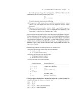
68 Chapter 2
where
,,mk km
U U is the shorthand notation for cross-correlation coefficient
()()mk
cc
R between the two spreading codes of channel
m
and channel
k
,
()i
A
is the amplitude of signal on channel i ,
()i
k
d
is the kth data symbol on chan-
nel
i , and
()i
k
Q
is the ith noise component. The effect of MAI is apparent,
and it is also clear that it can be potentially destructive. Assume for instance
that
1,2
0Uz (codes 1 and 2 are not orthogonal) and that
(2) (1)
AA : the
MAI term
(2) (2)
1,2 k
AdU in (2.150) may overwhelm the useful term
(1) (1)
k
Ad for
data detection of channel 1. This phenomenon is called the
near
far effect:
user 2 can be considered as located near the receiver in the BS, thus received
with a large amplitude, whilst user 1 (the one we intend to demodulate) is the
far user and is weaker than user 2. Generalizing to
N users, equations
(2.150) can be easily cast into a simple matrix form. If we arrange the cross-
correlation coefficients
,ik
U into the correlation matrix
1,2 1,
2,1 2,
,1 , 2
1
1
1
N
N
NN
UU
§·
¨¸
UU
¨¸
¨¸
¨¸
¨¸
UU
©¹
R
"
#%#
"
(2.151)
and if we also introduce the diagonal matrix of the user amplitudes
^
`
(1) (2) ( )
diag , , ,
N
AA A A , we have
zARdȞ (2.152)
where the column vectors
z , d , and Ȟ simply collect the respective sam-
ples of received signal, data, and noise. A simple multiuser detector is the
decorrelating detector that applies a linear transformation to vector z to
provide
N ‘soft’ decision variables relevant to the N data bits to be esti-
mated. Collecting such
N decision variables
()i
k
g
into vector g , the linear
joint transformation on the matched filter output vector
z
is just
1
gRz (2.153)
where
1
R is the decorrelating matrix, so that
11
gR ARdȞ Ad R Ȟ
^
`
12
12
diag , , ,
N
kk Nk
Ad Ad A d
c
Ȟ (2.154)
We have thus
2. Basics of CDMA for Wireless Communications 69
12
, , ,
T
N
kk k
gg g
ªº
¬¼
g (2.155)
where the superscript
T
denotes transposition,
() () () ()iiii
kkk
gAd
c
Q, and
()i
k
c
Q
is just a noise component. It is apparent that the MAI has been completely
cancelled
(provided that the correlation matrix is invertible) or, in other
words, the different channels have been
decorrelated. The drawback is an
effect of
noise enhancement owed to the application of the decorrelating ma-
trix
1
R
: the variance of the noise components in
c
Ȟ is in general larger than
that the components in
Ȟ . Therefore, the decorrelating detector works fine
only when the MAI is largely dominant over noise.
A different approach is pursued in the design of the
Minimum Mean
Square Error
(MMSE) multiuser detector: the linear transformation is now
with a generic
NNu matrix Z whose components are such that the MMSE
between the soft output decision variables in
g and the vector of the data
symbols is minimized
gZz, with Z such that
^
`
2
Emin gd , (2.156)
where
E{ } denotes statistical expectation. Solving for
Z
we have
1
22
Q
VZR A , (2.157)
with
2
Q
V
indicating the variance of the noise components in (2.150). The
MMSE detector tries to optimize the linear transformation both with respect
to MAI and to noise. If noise is negligible with respect to MAI, matrix
(2.157) collapses into the decorrelating matrix
1
R
. Vice versa, if the MAI is
negligible, the matrix
Z is diagonal and collapses just into a set of scaling
factors on the matched filters output that do not affect data decisions at all
(and in fact in the absence of MAI, the outputs of the matched filters are the
optimum decision variables without any need of further processing).
From this short discussion about MUD it is clear that in general such
techniques are quite challenging to implement, either because they require
non-negligible processing power (for instance, to invert the decorrelating or
the MMSE matrices), and because they also call for
a priori knowledge or
real time estimation of signal parameters, such as the correlation matrix. But
the potential performance gain of MUD had also an impact on the
standardization of 3G systems (UMTS in Europe), in that an option for short
codes in the downlink was introduced just to allow for the application of
such techniques in the BS [Ada98], [Dah98], [Oja98], [Pra98].
70 Chapter 2
How can MUD or related techniques be applied to the downlink of the
wireless system? Multiuser detection in the user terminal (the mobile phone)
has no meaning at all, since the UT is by definition a single-channel de-
modulator. Also, if channel equalization is good, hence channel distortions
are negligible, no MAI is experienced in the downlink, since the channeliza-
tion codes are orthogonal. Nonetheless, the downlink experiences inter-cell
interference, especially when the UT is close to a neighboring cell boundary.
Therefore a single-channel
Interference Mitigating Detector (IMD) is some-
thing the downlink would surely benefit from. Our previous consideration
about the two-sided effect of interference mitigation applies to the downlink
as well: the IMD can be used either to improve the quality of the link for a
given level of interference, or it can be used as an instrument to increase
network capacity for a given quality of the link.
How can we implement an IMD? We start by recalling the signal samples
at the chip matched filter output (see (2.117))
^`
1 1,1 1,1 intra inter
LL
mmmm
mm
yAd c b b n
(2.158)
where
intra
m
b
and
intra
m
b
denote the mth sample of the intra- and inter-cell in-
terference term, respectively. The two terms together make up a disturbance
term that is
independent of the useful signal component and adds up to the
background noise. Also, the total disturbance term
intra inter
mm m
Db b
is not
white as, in contrast,
m
n
is: the standard CR with the code matched filter (or
the despreader
accumulator cascade) is no longer optimum. It makes sense
therefore correlating the received signal samples with a set of coefficients
that is
not equal to the values of the spreading code
(1)
m
c . The decision vari-
able for the
kth data symbol on channel 1 will be thus equal to
1
11
0
1
L
kkLmm
m
zyh
L
¦
(2.159)
where the coefficients
m
h (from now on we will omit the superscript
(1)
for
simplicity) have to be designed according to a suited optimization rule.
Equation (2.159) can also be interpreted as the response to the input
m
y
of a
linear filter whose coefficients are just
m
h , downsampled to the symbol rate.
The simplest yet most effective criterion to design the filter coefficients is
again the MMSE rule, of course this time in a simplified single-channel ver-
sion with respect to (2.156)
2. Basics of CDMA for Wireless Communications 71
1
0
1
L
kkLmm
m
zyh
L
¦
,
with
01
, ,
L
hh
such that
^
`
2
1
Emin
kk
zd
(2.160)
We have to face an issue similar to that encountered in the MMSE MUD;
specifically, how to set the filter coefficients in order to solve the minimiza-
tion problem just stated. The solution of this issue leads to the concept of an
adaptive detector, whose coefficients are adapted in real time so as to mini-
mize the mean square error and thus build ‘on the fly’ an optimum linear de-
tector for the configuration of interference that the reference channel is ex-
periencing. We skip the detailed solution of the minimization problem
[Mad94] to report here the
recursive equation that, starting from arbitrary
values of the filter coefficients, allows the synthesis of the optimum detector
configuration
*
1
1
kk
kkzdk J hh y
, (2.161)
where the
L-dimensional vectors ()kh and ()ky
group the filter coefficients
at time
k and the received signal samples
kL m
y
,
0,1, , 1
mL
, respec-
tively
. In (2.161)
J
is the recursion step size, to be set a compromise be-
tween fast acquisition (large
J ) and small steady state fluctuations (small
J ). The drawback of the adaptive MMSE detector (2.161) is that recursive
adaptation of the coefficient vector
()kh calls for the knowledge of the
transmitted data
(1)
k
d
to compute the error
(1)
kkk
ezd
. This Data Aided
(DA) approach can be adopted if a set of pilot symbols is organized into a
preamble known to the receiver in an initial
training phase. At the end of the
training phase, the detector coefficients are ‘frozen’ and true data detection
starts. The detector operates thus in
Decision Directed (DD) mode. If MAI is
time varying, adaptation of the coefficients must be periodically carried out
each time a new preamble of known data appears in the signal framing. Of
course, this has an impact on the efficiency of the communication link, since
the preamble data does not convey any information, and contribute to the
overall data framing overhead. In addition, the recursion (2.161) may require
a large number of training symbols to attain a steady state condition (long
acquisition time), making the adoption of a data aided approach impractical.
Therefore it makes sense to revert to a
blind approach that does not re-
quire the insertion of any pilot symbols or preambles in the data stream. This
privileges framing efficiency and is also robust in terms of acquisi-
tion/reacquisition capability. The criterion to be adopted to satisfy this re-
quirement is the
minimization of the Mean Output Energy (Minimum MOE,
72 Chapter 2
MMOE) of the detector instead of the minimization of the squared error as
before
1
0
1
L
kkLmm
m
zyh
L
¦
,
01
, ,
L
hh
such that
^
`
2
Emin
k
z
. (2.162)
The rationale behind this criterion is that by minimizing the output en-
ergy the influence of MAI is minimized as well. Of course, we have to add
some additional constraints to this minimization problem, otherwise the so-
lution is a trivial one: all coefficients are equal to 0. The trick to avoid the
coefficients array
()kh
collapsing to 0 is the anchoring of its value to the
value it would have in the absence of interference. We know that with no
MAI the optimum receiver is the conventional correlator, so that in those
conditions
()k hc, where c is the L-dimensional array containing the code
chips
i
c
( 0, 1iL ! ) of the desired user. In the general case we set
kk hcx
(2.163)
where the constraint is that
c and ()kx be orthogonal: () 0
T
k cx (the su-
perscript
T
denotes matrix transposition). This is what we called the ‘anchor-
ing’, and this is also what prevents the coefficients from converging towards
0. This simple idea, which was introduced by Honig, Madhow, and Verdù
[Hon95], led to the development of what is called the
Extended, Complex-
valued, Blind, Anchored, Interference mitigating Detector
(EC-BAID). De-
sign of the detector (and adaptivity of the detector as well) is now transferred
to design and adaptivity of the code orthogonal vector
x.
In a sense, decomposition (2.163) can lead us to interpret the MMOE de-
tector as the superposition of
two detectors: the one characterized by the set
of coefficients
c is the conventional detector which is optimum for the
AWGN channel. The other ‘additional’ detector
x gives the additional fea-
ture of interference mitigation. It can be shown [Hon95] that the MMOE so-
lution for
x gives also the MMSE solution for h, i.e.,
MMSE MOE
hcx. The
resulting recursive equation for the vector
x is
*
1
T
k
kkzkk
L
ªº
J
«»
«»
¬¼
yc
xx y c
. (2.164)
The second term between brackets is the orthogonal projection of the vec-
tor of received samples onto the spreading code
c. So the EC-BAID is a
2. Basics of CDMA for Wireless Communications 73
modified MMOE linear detector operating on the received signal, sampled at
the chip rate,
m
y
to yield the symbol rate signal
k
z
as follows
1
T
ee
k
zkk
L
hy
, (2.165)
where ( )
e
ky is the extended 3L-dimensional array of the received signal
samples coming from
three symbol periods (i.e., the current period, the lead-
ing period, and the trailing period) whose elements are denoted as
e
i
y
1
0
1
e
k
kk
k
ªº
«»
«»
«»
¬¼
y
yy
y
and
() ()1 () 1
( ) , , ,
T
ikiLkiLkiLL
ky y y
ªº
¬¼
y
,
(2.166)
and
()
e
kh
is a similarly extended array of detector coefficients. It is appar-
ent that
extension refers to lengthening of the observation window of the
signal. Such extension is beneficial in terms of the interference rejection ca-
pability of the detector, especially for asynchronous MAI. The extended de-
tector can be effectively implemented for real time operation according to
the three-fold parallel architecture sketched in Figure 2-20, wherein the first
unit processes the (
k-1)th, the kth and the (k+1)th symbol periods for the
detection of the
kth symbol, the second unit processes the kth, the (k+1)th
and the (
k+2)th periods, for the detection of the (k+1)th symbol, and the third
unit processes the (
k+1)th, the (k+2)th and the (k+3)th periods, for the detec-
tion of the (
k+2)th symbol. Each detector unit has the structure outlined in
Figure 2-21. The final soft output data stream is obtained by sequentially se-
lecting one of the three detector outputs at the symbol rate 1/
T
s
by means of
a multiplexer. To better explain operations of the EC-BAID circuit in Figure
2-20 it is expedient to introduce a further clock reference ticking at what we
call the
Super-Symbol (SS) rate R
ss
= 1/(3T
s
), i.e., once every three symbols.
R
ss
is basically the operating rate of each of the three detectors. The output of
the
nth detector unit ( 1,2,3n ) is computed as
,
1
31 31
T
en e
zsn s sn
L
hy
, (2.167)
with
s running at super-symbol rate. To achieve blind adaptation, the com-
plex detector coefficients are anchored to the user signature sequence as out-
lined above.
74 Chapter 2
Figure 2-20. EC-BAID General Architecture.
Specifically, the extended detectors are characterized by the set of coeffi-
cients
1
,, ,
0
1
,,
n
en e en e en n
n
s
s
sss
s
ª
º
ªº
«
»
«»
«
»
«»
«
»
«»
¬¼
¬
¼
0x
hcxccx x
0x
, (2.168)
with the ‘anchor’ constraint 0
Tn
i
cx , 1, 0,1i , 1, 2,3n . By trivially
generalizing the recursive equation (2.164) we obtain the updating rule for
the interference-mitigating vectors of the three detectors
,,,
1
en en en
s
ss Jxxe, (2.169)
with
s ticking at the super-symbol rate, and where
1
,
0
1
*
*
,
31
31 ,1,0,1,
n
en n
n
T
i
n
ii
s
ss
s
sn
szs sn i
L
ªº
«»
«»
«»
¬¼
ªº
«»
«»
¬¼
e
ee
e
yc
ey c
(2.170)
2. Basics of CDMA for Wireless Communications 75
J is the adaptation step and the asterisk denotes complex conjugation. Equa-
tion (2.169) implicitly assumes that the three detector units are running inde-
pendently. More architectures can be devised wherein the error control sig-
nal for the update of vectors
,en
x
, whose elements are denoted as
e
i
x
, is
unique and is obtained as a combination of the partial errors
,en
e
[Rom00].
Figure 2-21. Internal structure of the three detectors in Figure 2-20.
An example of the interference mitigation capability of the EC-BAID is
given in Figure 2-22. We show in the chart the BER of a CDMA receiver
with asynchronous interference as a function of the number of concurrently
active users. The spreading factor is 64, the spreading codes are Walsh–
Hadamard with an Extended PN superimposed as scrambling code, and the
users delay are uniformly spaced over one symbol interval. The curve la-
beled BAID is obtained with a MMOE detector observing a single-symbol
ci
zk
J
-
+
+
+ +
-
76 Chapter 2
period, whilst the one labeled EC-BAID is obtained with the three-symbol
extended detector above. The superiority with respect to the conventional
correlation receiver is apparent, although it is also apparent that when the
number of channels gets close to the spreading factor even the IM detectors
cannot counteract MAI any longer.
The curves in Figure 2-22 also help to explain how the IM detectors can
be seen as a technological factor for increasing the network capacity in terms
of number of served users per cell. Assume that we place a QoS constraint in
terms of BER of the link,
2
10
just to be specific. The curve of the correla-
tion receiver in Figure 2-22 says that the maximum number of users in an
hypothetical cell with that spreading factor is restricted to about 7 (that is,
the value on the abscissas corresponding to the specified BER). The corre-
sponding figure on the EC-BAID curve at the same QoS is roughly 38, with
more than a 5-fold capacity increase!
10
-5
10
-4
10
-3
10
-2
10
-1
10
0
BER
10
-5
10
-4
10
-3
10
-2
10
-1
10
0
BER
6050403020100
Number of Users, N
6050403020100
Number of Users, N
BAIDBAID
EC-BAIDEC-BAID
CorrelatorCorrelator
Figure 2-22. Interference-mitigating capability of the EC-BAID.
6. A SAMPLE CDMA COMMUNICATION SYSTEM:
SPECIFICATIONS OF THE MUSIC TESTBED
As an example of a practical, we present hereafter the specifications of
the CDMA system envisaged in the framework of the MUSIC project, spon-
2. Basics of CDMA for Wireless Communications 77
sored by the ESA [MUS01]. Table 2-2 contains the specifications of the
CDMA signal generator, including signal format, programmability features
and physical characteristics of analog modulator. Concerning signal format,
we observe that the specifications indicate a DS/SS-QPSK transmission with
real spreading (Q-RS) which, according to Table 2-1, yields the best spectral
efficiency. Two different options are indicated for the set of spreading signa-
tures:
i) a composite code set made of the orthogonal WH sequences over-
laid by an extended PN for scrambling and cell/beam identification purposes,
and
ii) an extended version of the quasi-orthogonal Gold set, without over-
laying. In addition the specifications envisage a variable spreading factor
M
in order to make the generator capable of supporting multi-rate transmis-
sions. Since the modulation scheme is QPSK, the chip rate
c
R
of the useful
signal is given by
2
b
cs s
R
RMRnLRnL
, (2.171)
where
L is the signature code period,
n
represents the number of code peri-
ods within one symbol interval,
s
R
and
b
R
are the symbol rate and the bit
rate, respectively. The permitted values of
b
R
, L , and
c
R
, evaluated accord-
ing to (2.171), are shown in Table 2-3 (maximum chip rate
,max
2.048
c
R
Mchip/s). Full programmability is supported as far as data rates, multiple ac-
cess interference and additive noise are concerned. The aggregate CDMA
signal, made of the useful signal and MAI, produced by the MUSIC genera-
tor is described by the model in (2.109). Eventually the MUSIC generator
outputs an analog signal centered around the standard Intermediate Fre-
quency (IF)
IF
70f MHz . The bandwidth occupancy is (1 )
I
Fc
B
R D ,
where
0.22D is the roll off factor of the SRRC chip pulse shaping filters
and its maximum value turns out to be then
IF ,max
(1 ) 2.56
c
BR
D
MHz.
The receiver specifications are listed in Table 2-4. The CDMA signal
format specifications are the very same as in the transmitter case. In addi-
tion, some specifications are reported for the step size of the adaptive detec-
tor and for the synchronization, namely the spreading code acquisition time
and the Mean Time to Lose Lock (MTLL). The operating conditions, are ex-
pressed in terms of Signal to Noise Ratio (SNR) and/or Bit Error Rate
(BER). The specifications also report the overall maximum SNR degradation
allowed for the modem (implementation loss) owed to finite-precision
arithmetic digital processing and imperfect receiver synchronization. Finally,
the receiver specifications indicate two output formats: i) binary hard de-
tected Non-Return to Zero (NRZ) data, and ii) soft output samples repre-
sented by 4 bits.
78 Chapter 2
Table 2-2. Specifications of the MUSIC CDMA signal generator
Feature Symbol Specifications
Min. / max. channel
data rate
b
R
4 / 128 kb/s
Chip rate
c
R
Programmable 0.128, 0.256, 0.512, 1.024, 2.048 Mchip/s
accuracy: 1 Hz
Signature sequence
type
Option I: WH (traffic code) + E-PN (overlay)
Option II: E-Gold
Signature sequence
period
L
32, 64, 128 chips
Modulation/spreading
technique
QPSK / Balanced DS/SS with real spreading
(i.e., single-code)
Spreading factor
M
,1,,16
c
nL n !
Max. no. of
interfering channels
N L
Chip shaping
()
T
g
t Square root raised cosine with roll off 0.22
Random data
generator stream
Programmable on each CDMA channel with disable
capability
Interferers’ delay with
respect to the useful
channel
i
W
Programmable on each CDMA channel in the
range
0 Ly chip intervals, resolution 0.1 chip
interval
Interferers’ phase
offset with respect to
the useful channel
i
-
Programmable on each CDMA channel in the
range
0 360y degrees, resolution 1 degree
Interferers’ carrier
frequency offset with
respect to the useful
channel
i
f
'
Programmable on each CDMA channel in the
range
70r kHz, resolution 1 Hz
Useful channel to sin-
gle interferer
power ratio
/CI Programmable on each CDMA channel in the
range
10 dBr
, resolution 0.1 dB
IF carrier frequency
IF
f
70 MHz
Max. carrier
frequency uncertainty
on the useful channel
100r
Hz
Output signal level Programmable in the range
30 10 dBm
y , step 5 dBm
SNR
0
/
b
E
N Programmable in the range 3 30 dBy , step 1 dB
2. Basics of CDMA for Wireless Communications 79
Table 2-3. Bit and chip rates of the MUSIC CDMA signal format
Rb [kb/s] n
R
c [kchip/s]
@ L = 32
Rc [kchip/s]
@ L = 64
Rc [kchip/s]
@ L = 128
4 1 – 128 256
2 128 256 512
4 256 512 1024
8 512 1024 2048
16 1024 2048 –
8 1 128s 256 512
2 256 512 1024
4 512 1024 2048
8 1024 2048 –
16 2048 – –
16 1 256 512 1024
2 512 1024 2048
4 1024 2048 –
8 2048 – –
16 – – –
32 1 512 1024 2048
2 1024 2048 –
4 2048 – –
8 – – –
16 – – –
64 1 1024 2048 –
2 2048 – –
4 – – –
8 – – –
16 – – –
128 1 2048 – –
2 – – –
4 – – –
8 – – –
16 – – –
80 Chapter 2
Table 2-4. Specifications of the MUSIC CDMA receiver
Feature Symbol Specifications
IF carrier frequency
IF
f
70 MHz
Max. carrier frequency uncertainty 100r Hz
Input signal dynamics 40 10 dBm
y
Max. power unbalance between
traffic channels
6dBr
Min. input SNR
0
/
b
E
N -1 dB
Min. / max. channel data rate
b
R
4 / 128 kb/s
Chip rate
c
R
Programmable 0.128, 0.256, 0.512, 1.024,
2.048 Mchip/s with accuracy: 1 Hz
Signature sequence type Option I: WH (traffic code) + E-PN (over-
lay) – Option II: E-Gold
Signature sequence period
L 32, 64, 128 chips
Modulation/spreading technique QPSK / Balanced DS/SS with real spread-
ing (i.e., single-code)
Spreading factor
M
,1,,16nL n !
Max no. of interfering channels
NL
Chip shaping ( )
T
g
t Square root raised cosine with roll off 0.22
Adaptive detector step size
BAID
J
Programmable / adaptive with signal ampli-
tude
Min. SNR for acquisition and track-
ing @
0
/0dB
s
EN
0
min
c
E
N
ªº
«»
¬¼
–24 dB
Mean acquisition time @
min0
[/ ]
c
EN and
0
/0dB
s
EN
acq
T
< 4 sec
Acq. time with 99% @
min00
[/( )]
c
EN I
and
0
/0dB
s
EN
acq
T < 8 sec
MTLL for code/phase tracking @
BER=
2
810
L
L
T
4
310 sec!
Overall SNR degradation on
AWGN w.r.t. theory @
32
10 8 10BER
dd
0.5 dBd
Overall SNR degradation on
AWGN w.r.t. floating point simula-
tion, with ideal sync./EC-BAID
configuration @
32
10 8 10BER
dd
1dB
d
Baseband data output Binary hard detected NRZ and 4 bit soft
output, with NRZ clock signal
Chapter 3
DESIGN OF AN ALL DIGITAL CDMA
RECEIVER
After introducing the fundamentals of spread spectrum signaling and
CDMA we are now ready to delve deeply into the details of the system level
design of a DSP-based CDMA receiver. We will follow a bottom up
approach, starting from the multirate signal processing to be carried out in
the front end section of the demodulator, down to the specific subtleties of
the synchronization and signal detection algorithms. This will result in an
overall receiver architecture whose description and simulated performance
will be discussed in detail.
1. CDMA RECEIVER FRONT END
This Chapter contains a description of the main basic building blocks of a
DSP-based, multirate digital CDMA receiver. Starting from the architecture
of the digital downconversion stage in the MUSIC receiver’s Front End
(FE), it develops through a description of the signal interpolator to be used at
the output of the Chip Matched Filter (CMF), and describes the detailed
design of several sub-systems of an all digital CDMA receiver, with
particular emphasis on the multi-rate CDMA demodulator and to the
interference mitigation functionality.
1.1 Multi-Rate CDMA Signal
As already detailed in the previous Chapter, the signal at the output of the
MUSIC signal generator is centered around Intermediate Frequency (IF)
IF
70 MHzf and has a bandwidth occupancy
IF
(1 )
c
B
R D , where
82 Chapter 3
0.22D
is the roll off factor of the chip pulse shaping filter and
c
R
is the
chip rate. The latter ranges from
,min
128
c
R to
,max
2048 kchip/s
c
R , so
that he maximum signal bandwidth occupancy turns out to be
IF,max ,max
(1 ) 2.56 MHz
c
BR D . A sketch of the bandwidth occupancy of
the signal at the output of the signal generator is shown in Figure 3-1. Here,
as well as in the subsequent drawings, the spectral components of the signal
are represented as asymmetric with respect to
IF
f
. This is for illustrative
purposes only, and is not intended to be a faithful illustration of the actual
spectrum. The asymmetric spectral shape is helpful in identifying the
positive and negative frequency components of the received IF signal
spectrum during the baseband conversion process described in Section 1.3.
f (MHz)
70
BIF
-70
BIF
Figure 3-1. Spectrum of the IF signal.
1.2 Receiver Overall Architecture
The top level schematic of the CDMA receiver is shown in Figure 3-2.
For ease of discussion, the different functions performed by the receiver can
be partitioned as follows:
a) Digital Downconversion Unit (DDU);
b) Multirate Front End Unit (MRFEU);
c) Linear Interpolation Unit (LIU);
d) Code Timing Acquisition Unit (CTAU);
e) Chip Clock Tracking Unit (CCTU);
f) Automatic carrier Frequency Control Unit (AFCU);
g) Signal Amplitude Control Unit (SACU);
h) EC-BAID Unit, embedding Carrier Phase Recovery Unit (CPRU).
In addition the receiver also encompasses the Analog Signal
Conditioning Unit (ASCU) which performs band pass limiting and
amplitude control of the IF received signal prior to Analog to Digital
Conversion (ADC), and a digital processing unit devoted to SNIR (Signal to
3. Design of an All Digital CDMA Receiver 83
Noise plus Interference Ratio) estimation, denoted as SNIR Estimation Unit
(SEU). However, we remark that the design issues related to the latter two
additional units fall outside the scope of this book and therefore will not be
addressed here. The interested reader can find more details about signal
conditioning in reference [MUS01] and about SNIR estimation in references
[Gilch], [Div98], [MUS01].
1.3 From Analog IF to Digital Baseband
Concerning ADC, two different approaches are possible: asynchronous
and synchronous signal sampling.
In the first architecture the received signal is passed through an Anti-
Alias Filter (AAF) and is then fed to the ADC. The latter is controlled by a
free running oscillator, having no reference whatsoever with the clock of the
data signal. The ADC sampling rate
1/
s
T
is usually higher than the symbol
rate by an over sampling factor greater than 2. Timing correction is achieved
by interpolating the samples available at the matched filter output according
to the estimates of the timing error. Briefly speaking, the interpolator ‘re-
synthesizes’ those signal samples at the correct timing instants, that are in
general not present in the digitized stream. More details on the interpolator
sub-unit are reported in Section 2.2.
An alternative architecture involves synchronous signal sampling, and is
particularly useful with high data rate modems where oversampling is too
expensive or unfeasible altogether. Here, timing correction is accomplished
through a feedback loop wherein a Timing Error Detector (TED) drives a
Numerically Controlled Oscillator (NCO) that adaptively adjusts the clock of
the ADC, so that the digitized samples are synchronous with the data clock.
In the MUSIC receiver, the ADC rate is not critical, and the decision was
to resort to is asynchronous sampling. The received signal undergoes IF
filtering and is passed to the ADC wherein it is sampled at rate
s
f
. The value
of
s
f
is selected taking into account the following requirements:
i)
,max
4 4 2.048 Mchip/s 8.192 MHz
sc
fRt (to yield at least four
samples per chip);
ii) 2
n
s
f (to select from standard commercial quartz clocks);
iii)
IF IF
2
s
kf f Bt
,
IF IF
(1) 2
s
kf fB
,
(to ensure that the spectral
replicas arising from ADC do not overlap).
According to i) and ii), we set
14n and 16.384 MHz
s
f . Such value
of
s
f
was also found to meet condition iii) for an IF bandwidth
IF
2.56 MHzB
, with 9k .
84 Chapter 3
Figure 3-2. Top level schematic of the MUSIC receiver.
3. Design of an All Digital CDMA Receiver 85
The spectrum of the resulting sampled signal is shown in Figure 3-3,
where the replicas of the positive and negative frequency signal spectrum are
centered around
70 ,
ks
f
kf
(3.2.a)
70 ,
ks
f
kf
(3.2.b)
respectively, with
k an integer.
f (MHz)
70605040302010
4.464 20.848 37.232 53.616 70
B
IF
11.920
28.304
44.688
61.072
16.384
16.384
Figure 3-3. Spectrum of sampled IF signal after ADC.
Figure 3-4 zooms on the low frequency part of the spectrum, containing
the following spectral replicas
4
70 4 4.464 MHz,
s
ff
(3.3.a)
5
70 5 11.920 MHz,
s
ff
(3.3.b)
4
70 4 4.464 MHz,
s
ff
(3.3.c)
5
70 5 11.920 MHz.
s
ff
(3.3.d)
The sampled signal is then digitally I/Q downconverted to baseband by a
Digitally Controlled Oscillator (DCO) operating at the Digital IF (IFD)
IFD
4.464 MHzf
, as is sketched in Figure 3-5. The downconverted signal
86 Chapter 3
contains unwanted image spectra located at the frequencies
f
c
r
and
f
cc
r
as
follows
5IFD
7.456 MHz
f
ff
c
, (3.4.a)
4IFD
8.928 MHz
f
ff
cc
, (3.4.b)
5IFD
7.456 MHz
f
ff
c
, (3.4.c)
4IFD
8.928 MHz
f
ff
cc
. (3.4.d)
The unwanted image spectra located at
f
c
r
and
f
cc
r
will be rejected by
means of the (low pass) CMF. By normalizing with respect to the sampling
frequency
s
f
, we also get the normalized locations of the spectral images to
be rejected
7.456
0.455,
16.384
s
f
f
c
#
(3.5.a)
8.928
0.545.
16.384
s
f
f
cc
#
(3.5.b)
The basic and conceptual schematic of the I/Q downconverter is shown
in Figure 3-6, where the blocks labeled ‘CIC’ are in charge of decimation, as
detailed in Section 1.4. Figure 3-7 shows the implementation of the scheme
in Figure 3-6. (Digital) I/Q downconversion is implemented by resorting to a
Direct Digital Synthesizer (DDS) that drives a couple of real multipliers.
Particularly, the DDS is made up by a phase accumulator and a Look Up
Table (LUT) storing the sine and cosine samples.
The phase accumulator performs numerical integration of the digital
reference at frequency
IFD
f
, whose value is represented by the Frequency
Control Word (FCW) on
FCW
n bits, according to the following recursive
equation computed at the clock rate
s
f
1IFD
2
kk s
Tf
I I S , (3.6)
3. Design of an All Digital CDMA Receiver 87
where
1/
s
s
Tf is the sampling interval. The phase accumulator, which is
assumed to operate internally on
acc
n
bits, outputs a (sampled) ramp,
represented by
p
ha
n bits (with
p
ha
n <
acc
n
), whose slope is determined by the
digital FCW
IFD
f
. The
p
ha
n most significant bits of the accumulator are then
used to represent the phase
k
I
that is passed to a LUT which performs
sine/cosine generation and outputs the sequences
sin( )
k
I
and
cos( )
k
I
,
represented by
DCO
n bits. To do this the word representing the phase
k
I on
p
ha
n bits is used to address a ROM table containing
LUT
N
samples excerpted
from a period of a cosinusoid, quantized by
DCO
2
n
levels.
f (MHz)
2010
4.464
11.920
-10-20
-11.920
-4.464
Figure 3-4. Particular of Figure 3-3.
f (MHz)
2010
8.928
16.384
-10-20
-7.456
f (MHz)
2010
7.456
-10-20
-16.384
-8.928
16.384
-16.384
f (MHz)
2010
-10-20
-16.384
16.384
7.456-B
IF
/2-7.456+B
IF
/2
B
IF
/2
-B
IF
/2
Figure 3-5. Digital downconversion to baseband.
88 Chapter 3
ADC DCO
nADC
nDCO
CIC
n
CIC
nDCO
nADC
CIC
n
CIC
In-Phase
Quadrature
Figure 3-6. Basic block diagram of the I/Q digital downconversion to baseband.
ADC
DDS
nADC
nDCO
CIC
n
CIC
nDCO
nADC
In-Phase
Quadrature
CORDIC
CIC
n
CIC
CORDIC
LUT
Phase
Accumulator
FCW T sfIFD
nFCW
Clock fs
I
k
cos
sin
npha
nacc
Figure 3-7. Implementation of the I/Q digital downconversion to baseband.
Let us focus on the issue of quantization of
k
I , sin( )
k
I and cos( )
k
I , and
let us determine the number of required bits. First of all, assume for the
moment that the sine and cosine values have so many bits that the
quantization of
k
I is significant only. If the phase is quantized by
p
ha
n
bits
the unit circle is divided into
2
pha
n
phased increments, and the quantization
noise is uniformly distributed, so that the resulting RMS phase noise,
measured in fractions of a cycle, is
2
.
12
pha
n
I
V
(3.7)
3. Design of an All Digital CDMA Receiver 89
For instance, assuming 8 bits
pha
n , we have
3
1.1 10 cycles
I
V u ,
corresponding to an RMS value of 0.41 degrees, which seems adequately
small for the detection of QPSK-modulated signals to bear no appreciable
BER degradation. We remark however that accurate assessment of the actual
BER penalty associated with
p
ha
n can be carried out only by means of bit
true computer simulations, as is done in Section 5.2.
Now, let us make the reverse assumption that
k
I is delivered with
‘infinite’ precision, and that significant quantization takes only place in the
‘output’ values of the sine and cosine functions.
Denote also by q( )[ the
quantized versions of the infinite resolution value
[
. In this case, if the sine
and cosine functions are quantized by
DCO
n
bits the received signal will be
rotated by a phase amount given by
qsin
arctan
qcos
k
k
k
½
ªIº
°°
¬¼
c
I
®¾
ªIº
°°
¬¼
¯¿
, (3.8)
and, neglecting any amplitude fluctuation resulting from phase quantization,
the quantization error is
kkk
c
'I I I
. (3.9)
Following the analysis in [Gar88], the RMS value of this error, measured
in fractions of a cycle, is given by
DCO
2
12
n
I
V
S
. (3.10)
For
DCO
8 bitsn , we have
4
3.6 10 cycles
I
V u , corresponding to 0.13
degrees. From the two expressions above it turns out that the RMS
quantization error on the sine/cosine function values is
S times (i.e., about 4
times) larger than the RMS error caused by quantization of the phase (for the
same word length). Therefore, if the sine/cosine LUT outputs are quantized
by the same number of bits as the phase
k
I at the LUT input (
DCO
p
ha
nn ),
then the effect of quantization on the phase is dominant. Alternatively, if we
let
DCO
2
pha
nn (i.e., the sine/cosine outputs are represented by a word
shorter by two bits than the input phase word), then the LUT input and
outputs provide nearly equal contributions to the net quantization noise.
In addition to the issue of quantization noise owed to I/Q and/or phase
quantization, it is also necessary to determine the effect of finite length of a
word representation in the DCO. The phase rotator described above acts also
90 Chapter 3
as a frequency translator according to the following recursive algorithm,
which is inherently implemented by the DCO
1IFD
2mod2
kk s
Tf
I I S S, (3.11)
where
k
I is the instantaneous phase used to correct the incoming signal.
Scaling by
2S
we obtain
1
IFD
mod 1
22
kk
s
Tf
II
§·
¨¸
SS
©¹
. (3.12)
Denoting now by
k
- the (normalized) phase expressed in cycles
(
/2
kk
- I S, 0<1
k
d- ), we obtain
1IFD
mod 1
kks
Tf
- -
, (3.13)
or
IFD
mod 1
ks
kT f-
, (3.14)
which describes operation of the DCO. According to (3.13), at each sample
time the FCW (i.e., the normalized frequency
IFDs
Tf represented by
FCW
n
bits) is added to the previous contents of the accumulator, which operates on
acc
n bits. Overflow management of the accumulator is intrinsic to the
modulo-1 operation, with the accumulator contents regarded as a binary
fraction between 0 and 1 cycle. The exact value of the (normalized)
frequency
IFD
s
f
T is provided (at symbol time) by the Frequency Error
Detector (FED). Phase resolution can be made as fine as desired by
lengthening the accumulator word length, i.e., by increasing
acc
n . The Least
Significant Bit (LSB) of the FCW (
IFDs
Tf ) must be consistent with the LSB
of the accumulator. If there are
acc
n bits in the accumulator, the phase is
quantized into increments of
2
acc
n
cycle. Usually only the
p
ha
n Most
Significant Bits (MSBs) of the accumulator (with
p
ha acc
nnd
) are read out to
the subsequent sine/cosine LUT. The smallest frequency increment is
2
Hz,
2
acc
acc
n
s
n
s
f
f
T
' (3.15)
so improved frequency resolution can be obtained by lengthening the
accumulator (and the relevant FCW).
3. Design of an All Digital CDMA Receiver 91
In many practical applications a typical choice for the accumulator word
length is
32
acc
n
, so as to provide a phase resolution
32 10
2 2 2.33 10
acc
n
'- # u cycles, (3.16)
or, equivalently,
32 9
2 2 2 2 1.46 10
acc
n
'I S S # u rad, (3.17.a)
32 8
2 360 2 360 8.38 10
acc
n
'I u u # u deg. (3.17.b)
Concerning the frequency resolution we have
3
32
16.384 MHz
3.815 10
2
2
acc
s
n
f
f
' u Hz (3.18)
and
10
1
2.33 10 ,
2
acc
n
s
f
f
'
u
(3.19)
which is unnecessarily accurate for our purpose. By relaxing the
requirements about the resolution, we may consider a smaller accumulator
based on
8
acc
n bits, thus obtaining
83
2 2 3.91 10
acc
n
'- # u cycles (3.20)
83 2
2 2 2 2 3.91 10 2 2.45 10
acc
n
'I uS uS# u uS# u rad, (3.21.a)
83
2 360 2 360 3.91 10 360 1.41
acc
n
'I u u # u u # deg, (3.21.b)
8
16.384 MHz
64
2
2
acc
s
n
f
f' kHz, (3.22)
92 Chapter 3
3
1
3.91 10 .
2
acc
n
s
f
f
'
u (3.23)
The feasibility of an 8 bit accumulator will be verified later by means of
extensive bit true computer simulations. The phase at the accumulator output
can not have
p
ha acc
nn because of speed limitations in the access to the
LUT, therefore only the
p
ha
n MSBs of the accumulator (with
p
ha acc
nnd ) are
read out to the following sine/cosine LUT. According to the results
highlighted above, it is common practice to choose
DCO
2
pha
nn so as to
limit the truncation error. We assume that signal degradation is negligible if
the digital phase rotation of the samples is carried out by using 8 bit
sine/cosine coefficients (
DCO
8 bitsn ). This assumption seems rather
conservative and shall be verified, and possibly relaxed, by means of bit true
simulations. Under this hypothesis we have
10 bits
pha
n , and we can
address a number of
10
2 2 1024
pha
n
different phases. Considering the
symmetries of the sine and cosine functions, we can reduce the number of
elements stored in the LUT. Actually, it is sufficient to store in the LUT only
the samples (represented by 8 bits) of the sine in the interval 0–S/2
(corresponding to 1/4 of a cycle). Recalling that the phase resolution is 1024
samples per cycle, the LUT must contain only
LUT
1024 / 4 256N values.
A pictorial diagram of the LUT architecture is shown in Figure 3-8.
1.4 Decimation and Chip Matched Filtering
The received signal is sampled at the rate 1/ 16.384 Msample/s
ss
fT
,
and the number of samples per chip is therefore given by
16.384
,
s
s
cc
f
RR
Q (3.24)
whose possible values for the various chip rates are reported in Table 3-2.
Notice that chip matched filtering and the subsequent digital processing
operations (noticeably chip timing synchronization) require no more than 2
to 4 samples per chip interval. According to (3.24) the signal turns out to be
significantly oversampled for the lowest bit rates, and this would cause the
CMF to bear excessive complexity owing to the huge number of taps
required. Therefore decimation is in order so as to achieve the target
sampling rate of
4 sample/chip
s
n . The decimation factor to be applied is
16.384 4.096
4
ss
s
sc c c
f
nnR R R
Q
U
(3.25)