Adaptive Techniques for Dynamic Processor Optimization_Theory and Practice Episode 1 Part 8 ppsx
Bạn đang xem bản rút gọn của tài liệu. Xem và tải ngay bản đầy đủ của tài liệu tại đây (793.01 KB, 20 trang )
Chapter 6 Dynamic Voltage Scaling with the XScale Embedded Microprocessor 129
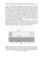
As a concrete example, assume the processor is running at 1 GHz and
V
DD
= 1.75 V. If half of the cycles are stalls waiting for the bus, as
determined by a combination of the total clock count, instructions
executed, and data dependency stall or bus request counts, the V
DD
can be
adjusted to 1.2 V (see Figure 6.2) and the core frequency reduced to 500
MHz. Useful work is then performed in a greater number of the (fewer
overall) core clock cycles. Referring to Figure 6.2, the power savings is
nearly 50% with the same work finished in the same amount of time.
6.2 Dynamic Voltage Scaling on the XScale Microprocessor
This section describes experimental results running DVS on the 180 nm
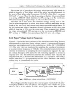
XScale microprocessor. The value of DVS is evident in Figure 6.3. Here,
the 80200 microprocessor is shown functioning across a power range from
10 mW in idle mode, up to 1.5 W at 1 GHz clock frequency. The idle
mode power is dominated by the PLL and clock generation unit. The
processor core includes the capacity to apply reverse-body bias and supply
collapse [10, 11] to the core transistors for fully state-retentive power-
down. The microprocessor core consumes 100 μW in the low standby
“Drowsy” mode [12]. The PLL and clock divider unit must be restarted
when leaving Drowsy mode. When running with a clock frequency of 200
MHz, the V
DD
can be reduced to 700 mV, providing power dissipation less
than 45 mW.
Figure 6.3 The value of dynamic voltage scaling is evident from this plot of the
80200 power and V
DD
voltage over time. The power lags due to the latency of the
measurement and time averaging.
4IMEARBITRARYSCALE
6
$$
6
#LOCK&REQUENCY-(Z0OWERM7
&REQUENCY
0OWER
AVESAMPLES
6OLTAGE
130 Lawrence T. Clark, Franco Ricci, William E. Brown
6.2.1 Running DVS
To demonstrate DVS on the XScale, a synthetic benchmark programmed
using the LRH demonstration board is used here. The onboard voltage
regulator is bypassed, and a daughter-card using a Lattice GAL22v10 PLD
controller and a Maxim MAX1855 DC-DC converter evaluation kit is
added. The DC–DC converter output voltage can vary from 0.6 to 1.75 V.
The control is memory mapped, allowing software to control the processor
core V
DD
.
The synthetic benchmark loops between a basic block of code that has a
data set that fits entirely in the cache (these pages are configured for write-
back mode) and one that is non-cacheable and non-bufferable. The latter
requires many more bus operations, since the bus frequency of 100 MHz is
lower than the core clock frequency, which must be at least 3× the bus
frequency on the demonstration board.
The code monitors the actual operational CPI using the processor PMU.
The number of executed instructions as well as the number of clocks, since
the PMU was initialized and counting began, are monitored. The C code,
with inline assembly code to perform low-level functions is
unsigned int count0, count1, count2;
int cpi() {
int val;
// read the performance counters
asm("mrc p14, 0, r0, c0, c0, 0":::"r0"); // read the PMNC register
asm("bic r1, r0, #1":::"r1"); // clear the enable bit
asm("mcr p14, 0, r1, c0, c0, 0":::"r1"); // clear interrupt flag, disable counting
// read CCNT register
asm("mrc p14, 0, %0, c1, c0, 0" : "=r" (count0) : "0" (count0));
asm("mrc p14, 0, %0, c2, c0, 0" : "=r" (count1) : "0" (count1));
asm("mrc p14, 0, %0, c3, c0, 0" : "=r" (count2) : "0" (count2));
return(val = count0);
}
int startcounters() {
unsigned int z;
// set up and turn on the performance counters
z = 0×00710707;
asm("mov r1, %0" :: "r" (z) : "r1"); // initialization value in reg. 1
asm("mcr p14, 0, r1, c0, c0, 0" ::: "r1"); // write reg. 1 to PMNC
}
Chapter 6 Dynamic Voltage Scaling with the XScale Embedded Microprocessor 131
Note that the code to utilize the PMU is neither large nor complicated. It
is also straightforward to implement the actual V
DD
and core clock rate
changes. To avoid creating a timing violation in the processor logic, the
core voltage V
DD
must always be sufficient to support the core operating
frequency. This requires that the voltage be raised before the frequency is
and conversely that the frequency be reduced before the voltage is. The
XScale controls the clock divider ratio from the PLL through writes to
CP14. The C code to raise the V
DD
voltage is
int raisevoltage() {
int i;
// raise the voltage first
if (voltage <= TOP_V) { // leave it alone
printf ("V at end of range ");
}
else {
voltage ;
*voltagep = voltage;
// adjusting the frequency
if (frequency < TOP_F) { // do nothing
frequency = uf[voltage];;
asm("mov r1, %0" :: "r" (frequency) : "r1");
asm("mcr p14, 0, r1, c6, c0, 0" ::: "r1");
}
}
return(voltage);
}
The code to lower the voltage is very similar. The supported clock
multipliers range from 3 to 11 [9]. The array uf[] is a lookup table of
appropriate voltages for each frequency. The PLD is programmed so that
the highest voltage of 1.7 V is programmed by setting the value to 0 and
higher values increase the voltage by 50 mV (for the first four entries) or
100 mV increments. The constant TOP_V = 0. For the
lowervoltage() function, an equivalent BOTTOM_V constant avoids
setting the voltage too low. No delay is required, since the coprocessor
register write forces the core clocks to be inactive for approximately 20 μs
while the PLL relocks to the new clock fraction—this is handled
automatically by the XScale core hardware. Excellent power supply
rejection ratio (PSRR) in the 80200 PLL allows the relock to occur in
132 Lawrence T. Clark, Franco Ricci, William E. Brown
parallel with the voltage movement. The code to lower the voltage is
similar, but as mentioned, the frequency is reduced before lowering the
voltage. Again, the PLL lock time, invoked before the MCR P14
instruction can finish, hides the latency of the voltage movement from the
software.
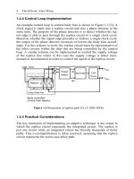
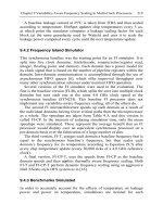
Figure 6.4 Simple DVS control heuristic using an estimate of the CPI as
determined by the PMU. The CPI is estimated for each time slice and VDD
adjusted if it is outside the dead-band parameters CPI_DB_high and
CPI_DB_low. Otherwise the V
DD
and clock frequency are unchanged.
Here, for illustration purposes, the control algorithm is very simple, as
shown in Figure 6.4. All but the “Execute time slice…” block would be
part of the OS. Behavior of the synthetic benchmark, using the code shown
above, is shown in Figure 6.5(a). Many complicated and hence more
optimal V
DD
control algorithms have been developed but are application
dependent and beyond the scope of this discussion. The frequency and
voltage are increased by one increment if the measured CPI is below the
predetermined value CPI_DB_high, and they are decreased by one
increment if the CPI is above another predetermined value CPI_DB_low.
It is left the same otherwise, i.e., the control dead-band is defined by the
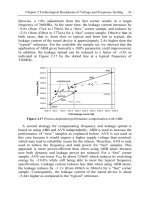
separation of the two values. Figure 6.5(b) shows the intervals more
closely. The intervals running the bus limited data access code are marked
by A, and the faster running (cacheable data) code is marked by B. The
distinct V
DD
voltage steps when the frequency and voltage are changed as
the data accesses move from one behavior to the other are evident.
Chapter 6 Dynamic Voltage Scaling with the XScale Embedded Microprocessor 133
Figure 6.5 Oscilloscope traces of V
DD
on the LRH test system. The system is
running a synthetic benchmark that modifies V
DD
based on the CPI as determined
by the PMU (a)–(d). The distinct steps in voltage with each software-controlled
clock rate and V
DD
change are evident. The V
DD
slew rate is shown in (e), where
the supply ripple can also be seen.
Adjusting the size of the control heuristic dead-band to be too small
causes the voltage to “hunt” when running the faster code, as evident in
Figure 6.5(c) section B since a stable CPI value between that which causes
an increase and that which causes a decrease is not found. This hunting
behavior is not efficient, since the PLL lock time is wasted for each 50 mV
V
DD
movement. It is therefore important to define a large enough stable
region and make DVS changes (monitor the CPI) infrequently enough to
keep the total voltage change time insignificant compared to the total
operating time. A further adjustment in the heuristic affects the minimum
usable voltage, by allowing still slower operation for the bus limited code.
A
A
A
A
B
B
B
A
B
A
B
(a)
Horizontal scale: 1 s/div
Horizontal scale: 400 ms/div
Horizontal scale: 400 ms/div
Horizontal scale: 200 ms/div
Horizontal scale: 20 us/div
(b)
(c)
(d)
(e)
134 Lawrence T. Clark, Franco Ricci, William E. Brown
Figure 6.5(e) shows the maximum slew rate for the large voltage change
from 1.0 to 1.7 V, which is the nearly vertical V
DD
movement near the end
of the trace in Figure 6.5(d). The core V
DD
is slightly over-damped, as
evident in Figure 6.5(e).
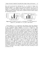
6.3 Impact of DVS on Memory Blocks
As mentioned in the introduction, some circuits may limit operation at low
V
DD
. Microprocessors and SOC ICs include numerous memories, usually
implemented with six transistor SRAM cells. In future devices, it is
expected that memory, and SRAM in particular, will dominate IC area
[13]. Unfortunately, SRAM has diminishing read stability [14] as
manufacturing processes are scaled down in size and transistor level
variations increase [15]. Lower V
DD
profoundly reduces SRAM read
stability, making it a primary limiting circuit when applying DVS.
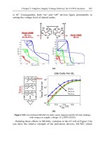
When the SRAM is read, the low storage node rises due to the voltage
divider comprised of the two series NMOS transistors in the read current
path, which includes one of the storage nodes. Monte Carlo simulations of
SRAM static noise margin are shown in Figure 6.6. As V
DD
is decreased,
the static noise margin (SNM) as measured by the smallest side of the
square with largest diagonal in the small side of the static voltage curves
(see Figure 6.6(a)) decreases as well. The large transistor mismatch due to
both systematic (intra-die) and random (within-die) variations cause
asymmetry in the SNM plot as shown in Figure 6.6(a). An IC contains
many SRAM cells, so the combination of worst-case systematic and
random variations can cause some cells to fail, significantly impacting the
manufacturing yield at low V
DD
. The simulated behavior of the SRAM
SNM vs. voltage, using Monte Carlo device variations to 5σ, is shown in
Figure 6.6(b). It is evident that the SRAM read margins are strongly
affected by the combination of transistor variation and reduced V
DD
.
Register file memory, which is also ubiquitous in microprocessors and
SOC Ics, does not suffer from reduced SNM when reading since the read
current path does not pass through the SRAM storage nodes. These
memories can scale with any core logic and can in fact operate effectively
well into subthreshold, i.e., they allow operation with V
DD
< V
th
. [16, 17].
6.3.1 Guaranteeing SRAM Stability with DVS
In the 180 nm process used for the XScale, the manufacturing yield is
negligibly impacted by SRAM read stability, even at V
DD
= 0.7 V when
Chapter 6 Dynamic Voltage Scaling with the XScale Embedded Microprocessor 135
only the two 32kB caches are considered. However, adding large SOC
SRAMs significantly affects the IC manufacturing yield at low V
DD
. The
solution used for the 180 nm “Bulverde” application processor SOC [18] is
to scale the XScale cache circuits with the dynamically scaling core and
SOC logic supply voltage, while operating the large SOC SRAM on a
fixed supply [19]. The SRAMs and their voltage domains are shown in
Figure 6.7. The SOC logic clock rate is 104 MHz or less depending on the
DVS point, while the core clock frequency scales from 104 MHz to over
Figure 6.6 SRAM SNM at various voltages (a). The mean and 5σ SNM from
Monte Carlo simulations (b) show vanishing SNM at low voltages. The XScale
SOC logic level shifts SRAM input signals and operates the SRAMs at a constant
voltage where SNM is maintained.
136 Lawrence T. Clark, Franco Ricci, William E. Brown
Figure 6.7 SRAMs and their voltage domains in the XScale core and in
the Bulverde application processor [20]. This diagram is greatly simplified
to emphasize the DVS vs. constant V
DD
domains.
500 MHz [18, 20]. A constant 1.1 V SRAM power supply voltage
(V
DDSRAM
) provides adequate access times for the slower SOC logic. In this
manner, the SOC and microprocessor core logic V
DD
employ DVS, but the
embedded SOC SRAM supply V
DDSRAM
is fixed. The fixed, higher
minimum V
DD
for the additional SOC SRAMs assures high manufacturing
yield with a low minimum V
DD
for DVS. The fixed SRAM supply voltage
also facilitates the low standby power Drowsy modes, which have a single
optimal V
DD
that must be sufficient to allow raising the NMOS transistor
source nodes toward V
DD
to apply NMOS body bias [11].
With two differing supply voltages, level shifting is required between
the memories and the SOC logic. The added level shifters degrade the
maximum performance, since they add delay. This is not an issue for low
V
DD
operation—the higher SRAM V
DD
makes them fast compared to the
surrounding logic operating at lower V
DD
. The problem is that the level
shifters slow the maximum clock rate of the design at high V
DD
by
injecting extra delay in the memory access path.
The Bulverde SOC memory level shifting scheme is shown in
Figure 6.8(a). To minimize the number of level shifters and limit the
complexity, the address ADD(1:m) and some control signal voltages are
translated to the different V
DDSRAM
power supply domain by the cross-
coupled level shifting circuit evident at the decoder inputs. This scheme
has the drawback that the word-line enable signal WLE, which is
essentially a clock, and the array pre-charge signal PRECHN must be level
Chapter 6 Dynamic Voltage Scaling with the XScale Embedded Microprocessor 137
shifted. The write and read column multiplexer control signals must also
be level shifted—for clarity, these circuits are not shown in the figure. The
differential sense amplifiers, which operate at the (potentially lower) DVS
domain supply voltage, automatically shift the SRAM outputs OUTDATA
to the correct voltage range. The sense timing signal SAE is also in the
DVS domain.
Figure 6.8 Level shifting paths to allow the SRAM supply voltage V
DDSRAM
to
remain constant while applying DVS to the surrounding logic. In (a) the level
shifters are placed at the SRAM block interface, while in (b) the level shifters are
at the storage array interface. In both cases, the sense amplifiers shift back to the
DVS domain.
138 Lawrence T. Clark, Franco Ricci, William E. Brown
Additional power can be saved by the scheme shown in Figure 6.8(b),
which shifts the voltage levels at the decoder outputs, i.e., the SRAM
word-line drivers. Here, the decoders reside in the scaled V
DD
domain and
fewer control signals must be level shifted to the V
DDSRAM
domain.
6.4 PLL and Clock Generation Considerations
In this section, the implications of DVS on microprocessor clocking are
considered. In the original 180 nm implementation, a simple approach was
taken—there are minimal changes to the PLL and clock generation unit to
support DVS. The feedback from the core clock tree to the PLL requires a
PLL relock time for each clock change. In the 90 nm prototype, the PLL
and clock generation unit was explicitly designed to support zero latency
clock frequency changes. Here, the PLL is derived from the I/O supply
voltage via an internal linear regulator. Hence, the PLL power supply is
not dynamically scaled with the processor core.
6.4.1 Clock Generation for DVS on the 180 nm 80200 XScale
Microprocessor
The clock generation unit in the 80200 is shown in Figure 6.9. The ½
divider provides a high quality, nearly 50% duty cycle output. The
feedback clock is derived from the core clock, to match the core clock (and
I/O clock, which is not shown) phase to the reference clock. Experiments
with PLL test chips showed that phase and frequency lock can be retained
during voltage movements, if the PLL power supply rejection ratio is
sufficient and the slew rate is well controlled [21,22]. This allows voltage
adjustment while the processor is running, as mentioned. However, a
change in the clock frequency changes the numerator in the 1/N feedback
clock divider. This causes an abrupt change in the frequency of the signal
PLL to relock to the new frequency.
The PLL generates a lock signal, derived from the charge pump activity.
Depending on the operating voltage, the PLL can achieve lock as quickly
as a few microseconds. However, a dynamic lock time makes customer
specification and testing more difficult—hence, a fixed lock time is used.
Another scheme, which allows digital control of the clock divider ratio
was developed for the 90 nm XScale prototype test chip.
Feedback Clk, which necessitates the
Chapter 6 Dynamic Voltage Scaling with the XScale Embedded Microprocessor 139
Figure 6.9 The 80200 PLL and clock generation scheme. The PLL must relock
for each frequency change, since the feedback divider ratio is altered. The clock
distribution network is much deeper than that indicated in the figure.
6.4.2 Clock Generation 90 nm XScale Microprocessor
The clock generation unit in the 90 nm XScale prototype microprocessor
[5] is shown in Figures 6.10 and 6.11. Placing the PLL, which is
implemented with the thin-oxide high-speed core transistors on the
regulated power supply V
DDPLL
reduces the jitter component caused by
power supply noise, which allows the core to operate at higher frequencies.
The low dropout (LDO) linear regulator is connected to the same voltage
as the I/O supply, which may be 1.8 V to 3.3 V. The LDO reduces the
V
DDPLL
voltage to the nominal core voltage value, while allowing the PLL
and clock generation unit to operate continuously through core voltage
changes. It also greatly improves the PLL PSRR, since it acts as a low-pass
filter as well as a level down-converter. The system bill of materials
(BOM) cost is not increased, since the PLL supply is the same voltage as
the I/O. It uses a separate supply pin, ideally with filtering for even greater
power supply noise rejection. The PLLs used in both the 180 nm and 90
nm XScale prototype designs discussed are based on the self-biased PLL
design presented in [23].
True on-the-fly DVS, with no time penalty for speed changes, is enabled
by having multiple separate dividers of the VCO clock for each SOC
function, as shown in Figure 6.11. Again, the VCO clock output of the
PLL is run at the twice maximum desired frequency to ensure a high-
quality clock with a 50% duty cycle, i.e., M in the 1/M divider is at least
two. Changes in the core, I/O or SOC clock frequencies, derived from the
1/M, 1/X, and 1/Y dividers, respectively, are achieved without affecting
the PLL lock since the PLL feedback is not derived from any of these
counters. The feedback clock divider sets 1/N to the appropriate value for
the required maximum VCOout frequency.
140 Lawrence T. Clark, Franco Ricci, William E. Brown
Figure 6.10 Regulated supply PLL used on the 90 nm XScale prototype [5]. The
PLL power is supplied through a LDO regulator, which improves the PSRR and
makes the PLL supply voltage independent of that of the processor core.
Figure 6.11 PLL and clock distribution network for the 90 nm XScale prototype
allowing true on-the-fly clock speed changes. The δ delay in the feedback path is
necessary to match insertion delays between the I/O and reference clock.
The 1/N, 1/M, 1/X, and 1/Y divider blocks in Figure 6.11 are digital
counters of the PLL voltage controlled oscillator (VCO) output. These
signals are compared to configuration bits to determine when output clock
transitions are to be generated. The δ delay is programmable using the
standard JTAG interface, to assure the edges of the I/O clock are aligned
with those of the core clock.
The synchronization of a frequency change is achieved by first latching
in the divider change request on the falling edge of the externally
generated reference clock signal RefClk. Then, the new values are latched
Chapter 6 Dynamic Voltage Scaling with the XScale Embedded Microprocessor 141
into the VCO domain by comparing the counter values in the VCO control
latches to their inputs and enabling the VCO domain latch clocks to
transition for one VCO clock cycle when a difference is detected. Finally,
the comparison values are transferred to the divider comparators precisely
one VCO cycle before the following synchronized rising edges of the M,
X, and N dividers. This ensures that the derived clocks do not glitch and
that the transition from one frequency to another occurs simultaneously in
all domains. The on-the-fly frequency changes are shown in Figure 6.12.
Here, the core frequency switches from 500 MHz (labeled A) down to 125
MHz (labeled B) and then back up to 250 MHz in the section labeled C.
As evident in the figure, the transitions can occur closely spaced, and the
PLL operation remains unchanged, i.e., the frequency changes occur
without re-synching or relocking the PLL.
Since all the dividers are eventually synchronized on the final output
generated by the 1/N divider, a global reset from the 1/N divider is
logically OR-ed into the local reset of each of the other dividers. Loss of
synchronization at high speeds, caused by critical timing paths in the clock
generation logic that includes the reset signal, is thus prevented.
Figure 6.12 Simulated clock waveforms showing true on-the-fly clock frequency
changes. Different frequencies are indicated by sections A, B, and C. Short clocks
(glitches) in the generated clocks must be avoided while changing the divider
ratios. The feedback clock (not shown) is a divided version of CoreClk, matching
RefClk in frequency and phase.
220
Time(ns)
B
CoreCIK
RefCIK
CA
240 260 280 300 320
VCOout
142 Lawrence T. Clark, Franco Ricci, William E. Brown
6.5 Conclusion
This chapter has described DVS on the XScale micro-architecture. The
XScale circuits, micro-architectural and architectural level supports for
DVS have been described. Supporting DVS requires that the software
running on the processor be able to predict the future workload to adjust
the V
DD
appropriately, based on past operations. DVS requires
architectural support for not only dynamic frequency and voltage
adjustments but also for real-time performance monitoring.
Increasing transistor mismatch, which is exacerbated by aggressive
transistor scaling, has made low-voltage SRAM operation problematic.
Consequently, ICs employing DVS must comprehend the SRAM yield
impact. In this chapter, the methods used to provide SRAM stability, i.e.,
level-shifting and operation of the embedded SRAMs at higher single
power supply voltage, in the XScale SOCs have been described. The
relatively small first-level cache SRAMs maintain full high V
DD
performance by their inclusion in the DVS domain. To support DVS on
future scaled manufacturing processes, which exhibit even greater
transistor variability, separate power supplies may be needed for all
SRAMs.
DVS can be implemented with minimal clock level support, e.g.,
requiring the PLL to relock at each frequency change. Better performance
and finer granularity clock changes can be obtained with an improved
clocking scheme which does not place the core clocks in the PLL feedback
loop. This implementation, used in the 90 nm XScale processor prototype,
allows clock frequency changes with no wasted time for re-
synchronization.
References
[1] Clark, L, et al., “An embedded microprocessor core for high performance
and low power applications,” IEEE Journal of Solid-State Circuits, Vol. 36,
No. 11, pp. 498–506, November 2001.
[2] Montonarro, J, et al., “A 160 MHz, 32b 0.5W CMOS RISC microprocessor,”
IEEE Journal of Solid-state Circuits, vol. 31, pp. 1703–1714, November
1996.
[3] Weiser, M, Welch, B, Demers, A, Shenker, S, “Scheduling for reduced CPU
energy,” Proceedings of the Fisrt Symposium on Operating Systems Design
and Implementation, November, 1994.
Chapter 6 Dynamic Voltage Scaling with the XScale Embedded Microprocessor 143
[4] Pering, T, Burd, T, Broderson, R, “The simulation and evaluation of
dynamic voltage scaling algorithms,” Proceedings of International
Symposium on Low Power Electronics, pp. 76–81, August 1998.
[5] Ricci, F, et al., “A 1.5 GHz 90-nm embedded microprocessor core,” VLSI
Circuits Symposium on Technology Design, pp. 12–15, June 2005.
[6] Sakurai, T, Newton, A, “Alpha-power law MOSFET model and its
applications to CMOS inverter delay and other formulas,” IEEE Journal of
Solid-State Circuits, Vol. 25, No. 2, pp. 584–594, April 1990.
[7] Mudge, T, “Power: A first-class architectural design constraint,” Computer,
Vol. 34, No. 4, pp. 52–58, April 2001.
[8] Intel 80200 Processor based on Intel XScale Microarchitecture Developers
Manual, November 2000.
[9] Intel XScale Core Developers Manual, December 2000.
[10] Clark, L, Deutscher, N, Ricci, F, Demmons, S, “Standby power management
for a 0.18-μm microprocessor,” Proceedings of International Symposiums on
Low Power Electronics, pp. 7–12, August 2002.
[11] Clark, L, Morrow, M, Brown, W, “Reverse body bias for low effective
standby power,” IEEE Transactions on VLSI Systems, Vol. 12, No. 9, pp.
947–956, September, 2004.
[12] Morrow, M, “Micro-architecture uses a low power core,” Computer, p. 55,
April 2001.
[13] ITRS roadmap. Online at www.itrs.org.
[14] Seevinck, E, List, F, Lohstroh, J, “Static noise margin analysis of MOS
SRAM cells,” IEEE Journal of Solid-State Circuits, Vol. 22, No. 5, pp. 748–
754, October 1987.
[15] Bhavnagarwala, A, Tang, X, Meindl, J, “The impact of intrinsic device
fluctuations on CMOS SRAM cell stability,” IEEE Journal of Solid-State
Circuits, Vol. 36, No. 4, pp. 658–665, April 2001.
[16] Chen, J, Clark, L, Chen, T, “An ultra-low-power memory with a
subthreshold power supply voltage,” IEEE Journal of Solid-State Circuits,
Vol. 41, No. 10, pp. 2344–2353, October 2006.
[17] Calhoun, B, Chandrakasan, A, “A 256-kb 65-nm Sub-threshold SRAM
design for ultra-low-voltage operation,” IEEE Journal of Solid-State
Circuits, Vol. 42, No. 3, pp. 680–688, March 2007.
[18] Intel PXA27× Processor Family Developers Manual.
[19] US patent 6,650,589: “Low Voltage Operation of Static Random Access
Memory,” November 18, 2003.
[20]
Intel PXA27× Processor Family Power Requirements.
[21] US patent 6,519,707: “Method and Apparatus for Dynamic Power Control of
a Low Power Processor,” February 11, 2003.
[22] US patent 6,664,775: “Apparatus Having Adjustable Operational Modes and
Method Therefore,” December 16, 2003.
[23] Maneatis, J, “Low-jitter process-independent DLL and PLL based on self-
biased techniques,” IEEE Journal of Solid-State Circuits, Vol. 31, No. 11,
pp. 1723–1732, November 1996.
Chapter 7 Sensors for Critical Path Monitoring
Alan Drake
IBM
7.1 Variability and Its Impact on Timing
Modern processes are becoming more sensitive to noise [25]. In addition
to technology parameters having larger variation with each new technol-
ogy generation [1], [20], timing sensitivity to such environmental condi-
tions as temperature [19], [31], aging [3], workload [19], [13], cross-talk
noise in wires [18], NBTI [12], and many other effects is increasing.
Noise processes that effect timing are described as random or system-
atic, and they are measured from die to die and within die [6], [32]. Ran-
dom noise is less dependent on the integrated circuit’s design than system-
atic noise and it is characterized by a number of statistics such as its mean
and standard deviation. Systematic noise results from characteristics of the
manufacturing process or from the physical design and can be predicted
once the underlying process causing the variation is understood. For ex-
ample, the wire thickness in technologies that use copper metallization is
dependent on the wire density and wire width [21]. Once the source of sys-
tematic variation is identified, designs can be adjusted or processing can be
modified to reduce the variation [27], [1]. Die-to-die noise measurements
measure the statistical difference between separate integrated circuit die
and inter-die noise is measured within a single die [5], [4].
The increasing timing uncertainty due to noise processes as technology
scales is creating a need for on-chip timing sensors that can be explained
using Figure 7.1. During the early design stages of the integrated circuit,
assuming it is a microprocessor, an iterative process is used to develop the
architecture to meet the performance targets of the intended application
.
Once the architecture is defined, the microprocessor passes through logic,
A. Wang, S. Naffziger (eds.), Adaptive Techniques for Dynamic Processor Optimization,
DOI: 10.1007/978-0-387-76472-6_7, © Springer Science+Business Media, LLC 2008
146 Alan Drake
circuit, and physical design. Models describing the timing of the target
technology are used to predict the timing of the microprocessor during its
design phases. Once timing is met, the processor is fabricated and tested. If
performance targets are met, the microprocessor will be binned into per-
formance categories and sold. If not, the design cycle must iterate at some
point to fix the errors.
When the timing models can accurately predict the performance of the
microprocessor, even when within-die variation is significant, adding a de-
sign margin and binning is sufficient for determining the performance of
the microprocessor [32]. However, as sensitivity to environmental condi-
tions increases, the needed margins to ensure functionality cause valuable
performance to be lost. Because much of the timing variation (caused by
such things as power supply noise and temperature shifts) is related to
workload, it can be considered systematic noise and compensated for using
dynamic voltage and frequency scaling (DVFS).
Define Architecture
Meets
Performance
Target
Pass Timing
Fabrication
Functional Testing
Meets
Performance
Target
Bin Parts
Logic/Circuit/Physical
Design
Define Process
Extract Process Model
Create Timing Model
Figure 7.1 A simplified design flow is shown for a large-scale integrated circuit.
Emphasis is placed on the development of the target performance and testing to
ensure that performance is met.
Chapter 7 Sensors for Critical Path Monitoring 147
DVFS is typically used to optimize the power/performance of a micro-
processor [7], [11], [26], [24], but if the DVFS system can sense a change
in temperature, workload, etc., then it can compensate for environmental
noise and recover some of the design margin [22]. For DVFS to be func-
tional, it must have a means to determine the operating point of the micro-
processor. This can be done using workload estimates and look-up tables,
but this is usually expensive in terms of calibration time and complexity.
Another solution, especially when dealing with fast environmental changes
like supply voltage noise, is to use on-chip sensors to monitor the operat-
ing condition. Such sensors, typically called critical path monitors, can
provide real-time performance information to DVFS systems with a sim-
pler calibration. The critical path is used because it is the benchmark of
timing and is most sensitive to environmental conditions. In addition to
providing real-time timing analysis, critical path monitors are extremely
useful as an aid in testing microprocessors. Since there is a cost overhead
to including critical path monitors, they must provide better performance
than just binning and margining by themselves. This chapter will describe
in detail the design of critical path monitors as real-time sensors providing
output to DVFS systems.
7.2 What Is a Critical Path
As discussed in the introduction, the timing for an integrated circuit is de-
termined during the design phase based on performance needs, power dis-
sipation, technology limitations, and design architecture. Once the cycle
time has been determined and design begins, a number of timing paths
within the integrated circuit emerge whose timing exceeds the cycle time.
These paths, called critical paths, must be retimed to meet the cycle time.
Part of the timing distribution of each path will exceed the cycle time as
shown in Figure 7.2. An equation for the delay of a critical path, including
sources of timing variation, is given in the following equation:
setupdd
TTTTTTT −−>+++
θθθθ
δ
δ
δ
δ
21
,
(7.1)
where T
d
is the path delay,
δΤ
θ
1
and
δΤ
θ
2
are the jitter in the sending and
receiving clock edges, T
θ
is the clock period, δT
θ
is the clock jitter, and
T
setup
is the latch setup time [32]. To ensure that all critical paths meet tim-
ing requirements, T
θ
must be increased to meet the following equation:
setupdd
TTTTTTmT −−<+++
θθθθ
δ
δ
δ
δ
σ
)(
21
,
(7.2)
148 Alan Drake
ter of the critical path timing and m is a multiplier determining the number
of standard deviations of error that are required for appropriate yield [32].
A large value of m (which is an expression of design margin) decreases not
only the probability of timing failure but also the integrated circuit’s per-
formance. As shown by the process spreads that overlap the cycle time in
Figure 7.2, the distribution of the critical path timing will exceed the cycle
time for all but the largest m (increasing m moves the cycle time to the left
on the graph). Because integrated circuits are sensitive to environmental
conditions, at a given operating point, the timing of one or more of the
paths may exceed the cycle time, causing a timing failure. Critical path
monitors are a way to provide feedback to the integrated circuit when criti-
cal paths may be approaching the cycle time so that the DVFS system can
respond appropriately to prevent a system failure.
7.3 Sources of Path Delay Variability
There are a number of noise processes that cause timing variability in an
integrated circuit. It is important to understand these processes and their
effect on the number and location of critical path monitors.
Path Delay
Path Delay Probability Distribution
←Cycle Time
Figure 7.2 Representative probability distribution of critical paths in a microcir-
cuit showing placement of the cycle delay. The location of the cycle time in the
process spread is determined by the desired yield.
where )(
21
θθ
δδδσ
TTT
d
++ is the standard deviation of the combined jit-
Chapter 7 Sensors for Critical Path Monitoring 149
7.3.1 Process Variation
Random, uncorrelated variations [1] cause two transistors carefully
matched and sitting next to each other to operate differently. Because of
this, a large-enough number of critical path monitors is needed to capture
meaningful estimates of the mean and standard deviation of the random
variations. Fortunately, the effect of random variation on delay is reported
to be small [32] since these variations average out, so they are not a driver
in determining the needed number of critical path monitors.
Systematic variations [20], which may also be random, are correlated
and make a smooth transition across a die or a wafer. If there is little
within die variation, then a single critical path monitor per die will be suf-
ficient to capture the die-specific timing variation. For die that has signifi-
cant inter-die variation, because the variation is correlated, critical path
monitors located near the circuits being monitored should be sufficient to
capture the systematic variation. The actual number of needed critical path
monitors will depend on how the noise process varies, but for large micro-
processors that only have on the order of tens of critical paths, only a few
critical path monitors are needed as long as they are located close to the
critical paths to capture the systematic variation.
7.3.2 Environmental Variation
Environmental noise processes are a function of the operating point of the
microprocessor. Some timing variations, such as clock jitter, clock skew,
path jitter, aging, and NBTI, have an uncorrelated, random component. A
single critical path monitor can track these random changes if sampled
over time as they will have a zero mean and constant variance across the
integrated circuit. Random, uncorrelated variation accounts for a small
portion of the variation in timing caused by environmental conditions [32],
so most timing variation is a result of the workload of the integrated circuit
[9], [33]. All of the environmental noise processes listed above with the
addition of temperature and power supply noise correlate directly to the
power consumed in the integrated circuit, which is a function of the work-
load of the circuit. In order to correctly monitor timing, critical path moni-
tors must be located close enough to where the noise is occurring to detect
its effect on critical path timing. Each of the environmental effects has a
different time and spatial constant that determines how many sensors are
needed to measure how the critical path’s timing responds.
Temperature [34], [16] resolves on the order of milliseconds and has a
spatial constant around 1mm: the temperature in any 1mm square is