Giáo trình CÔNG NGHỆ VI ĐIỆN TỬ - Chương 5 pps
Bạn đang xem bản rút gọn của tài liệu. Xem và tải ngay bản đầy đủ của tài liệu tại đây (657.35 KB, 9 trang )
Chương 5:Công nghệ mạch tích hợp
22
Chương 5
CÔNG NGHỆ MẠCH TÍCH HỢP
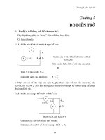
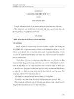
5.1. Các bước thiết kế IC
Hình 5.1 Các bước thiết kế tạo IC
Ý tưởng
Thiết kế kiến trúc
Thiết kế Logic
Thiết kế vật lý
Sản xuất
Chip mới
Chương 5:Công nghệ mạch tích hợp
23
5.2. Các bước chế tạo IC
Chương 5:Công nghệ mạch tích hợp
24
5.3. Quy tắc layout vi mạch
Chương 5:Công nghệ mạch tích hợp
25
Chương 5:Công nghệ mạch tích hợp
26
Chương 5:Công nghệ mạch tích hợp
27
Chương 5:Công nghệ mạch tích hợp
28
Chương 5:Công nghệ mạch tích hợp
29
5.4. Công nghệ IC:
5.4.1. Old Technologies:
1 Bipolar Diode Transistor Logic
2 Bipolar Diode Transistor Zener Logic
3 Bipolar Planar Transistor Transistor Logic
4 Basic steps in Planar Technology:
4.1 Buried Layer
4.2 Isolation
4.3 Collector
4.4 Base
4.5 Emitter
4.6 Contact
4.7 Oversized Contact – when needed
4.8 Metal
4.9 Passivation (Vapox)
5 Metal Gate CMOS – Diffusion Technique
(N- or P-Channel MOS are discrete)
5.1 P-Well
5.2 P+ Active Area
5.3 N+ Active Area
5.4 Gate
5.5 Contact
5.6 Oversized Contact – when needed
5.7 Metal
5.8 Passivation (Vapox)
5.4.2. Recent or Current Technologies:
1 Bipolar Planar Technology
2 Metal Gate CMOS – with Implantation Technique
3 Silicon Gate CMOS – with Implantation Technique
Chương 5:Công nghệ mạch tích hợp
30
3.1 N-Well
3.2 Active Area
3.3 Field Doping
3.4 Capacitor Implant
3.5 Gate Oxide
3.6 High Resistivity Poly Masking
3.7 P+ Implant (with P- Implant, optional)
3.8 N+ Implant (with N- Implant, optional)
3.9 Contact
3.10 Metal 1
3.11 Via (optional)
3.12 Metal 2 (optional)
3.13 Passivation (Vapox)
Usually 15 masks (up to 18 masks)
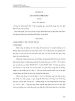
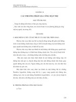
Cấu trúc BiCMOS
Normal
SiO
2
Emitter Base Collector Drain Gate
Source
Body
Aluminum
p
p
n
+
n
+
n
n
+
p p
p p
n
+
Thin
gate oxide
Epitaxal layer
Buried layer
p
Substrate
npn bipolar transistor
p-channel MOSFET