Electric Circuits, 9th Edition P63 ppt
Bạn đang xem bản rút gọn của tài liệu. Xem và tải ngay bản đầy đủ của tài liệu tại đây (751.63 KB, 10 trang )
596 Active Filter Circuits
15.7 a) Using only three components from Appendix H,
design a low-pass filter with a cutoff frequency
and passband gain as close as possible to the
specifications in Problem 15.6(a). Draw the cir-
cuit diagram and label all component values.
b) Calculate the percent error in this new filter's
cutoff frequency and passband gain when com-
pared to the values specified in Problem 15.6(a).
15.8 Design an op amp-based high-pass filter with a cut-
off frequency of 4 kHz and a passband gain of 8
using a 250 nF capacitor.
a) Draw your circuit, labeling the component val-
ues and the output voltage.
b) If the value of the feedback resistor in the filter
is changed but the value of the resistor in the
forward path is unchanged, what characteristic
of the filter is changed?
15.9 The input to the high-pass filter designed in
Problem 15.8 is 250 cos ot mV.
a) Suppose the power supplies are
±V
cc
.
What is
the smallest value of V
cc
that will still cause the
op amp to operate in its linear region?
b) Find the output voltage when
a)
= (o
c
.
c) Find the output voltage when
u>
= 0.2&><).
d) Find the output voltage when w = 5ft>
0
.
15.10 a) Use the circuit in Fig. 15.4 to design a high-pass
filter with a cutoff frequency of 8 kHz and a
passband gain of 14 dB. Use a 3.9 nF capacitor in
the design.
b) Draw the circuit diagram of the filter and label
all the components.
15.11 Using only three components from Appendix H,
design a high-pass filter with a cutoff frequency and
passband gain as close as possible to the specifica-
tions in Problem 15.10.
a) Draw the circuit diagram and label all compo-
nent values.
b) Calculate the percent error in this new filter's cut-
off frequency and passband gain when compared
to the values specified in Problem 15.10(a).
Section 15.2
15.12 The voltage transfer function for either high-pass
prototype filter shown in Fig. P15.12 is
Figure P15.12
C = IF
If
R = l a v,
(a)
R
= \a
L =
1
H v
(b)
15.13 The voltage transfer function of either low-pass
prototype filter shown in Fig. P15.13 is
H(s)
1
s + 1
Show that if either circuit is scaled in both magni-
tude and frequency, the scaled transfer function is
H'(s)
1
(s/k
f
) + 1
+
C =
1
F v„
(a)
L= 1H
R =
1
fl v
(b)
H(s) =
s + 1
15.14 The voltage transfer function of the prototype
bandpass filter shown in Fig. P15.14 is
Show that if either circuit is scaled in both magni-
tude and frequency, the scaled transfer function is
H'(s) =
{s/kf)
(s/k
f
) + 1
H(s)
s
2
+
Q
s + 1
Problems 597
Show that if the circuit is scaled in both magnitude
and frequency, the scaled transfer function is
!)(±
H>(s)
Figure P15.14
<h
+ 1
C=1F
L = 1H
R =^ v
0
15.15 a) Specify the component values for the prototype
passive bandpass filter described in Problem 15.14
if the quality factor of the filter is 20.
b) Specify the component values for the scaled
bandpass filter described in Problem 15.14 if
the quality factor is 20; the center, or resonant,
frequency is 40 krad/s; and the impedance at
resonance is 5 kft.
c) Draw a circuit diagram of the scaled filter and
label all the components.
15.16 An alternative to the prototype bandpass filter
illustrated in Fig. P15.14 is to make m
0
= 1 rad/s,
R = 1 ft, and L = Q henrys.
a) What is the value of C in the prototype
filter circuit?
b) What is the transfer function of the
prototype filter?
c) Use the alternative prototype circuit just described
to design a passive bandpass filter that has a qual-
ity factor of 16, a center frequency of 25 krad/s,
and an impedance of 10 kft at resonance.
d) Draw a diagram of the scaled filter and label all
the components.
e) Use the results obtained in Problem 15.14 to
write the transfer function of the scaled circuit.
DESIGN
PROBLEM
15.17 The passive bandpass filter illustrated in Fig. 14.22
has two prototype circuits. In the first prototype
circuit, co
0
= 1 rad/s, C = 1 F, L = 1 H, and
R = Q ohms. In the second prototype circuit,
co
0
= 1 rad/s, R = 1 ft, C = Q farads, and
L = (1/(2) henrys.
a) Use one of these prototype circuits (your
choice) to design a passive bandpass filter that
has a quality factor of 25 and a center frequency
of 50 krad/s. The resistor R is 40 kft.
b) Draw a circuit diagram of the scaled filter and
label all components.
15.18 The transfer function for the bandreject filter
shown in Fig. 14.28(a) is
s
2
+
H(s)
1
LC
'.I
l$
LC
Show that if the circuit is scaled in both magnitude
and frequency, the transfer function of the scaled
circuit is equal to the transfer function of the
unsealed circuit with s replaced by
(s/kf),
where kf
is the frequency scale factor.
15.19 Show that the observation made in Problem 15.18
with respect to the transfer function for the circuit
in Fig. 14.28(a) also applies to the bandreject filter
circuit (lower one) in Fig.
14.31.
15.20 The passive bandreject filter illustrated in
Fig. 14.28(a) has the two prototype circuits shown
in Fig. P15.20.
a) Show that for both circuits, the transfer function is
H(s) =
s
2
+ l
s
2
+ ( - )s + 1
b) Write the transfer function for a bandreject fil-
ter that has a center frequency of 50 krad/s and
a quality factor of 5.
Figure PI5.20
-pvQ;
(b)
15.21 The two prototype versions of the passive band-
reject filter shown in Fig. 14.31 (lower circuit) are
shown in Fig. P15.21(a) and (b).
Show that the transfer function for either ver-
sion is
H(s)
s
2
+ 1
s
2
+
s + 1
598 Active Filter Circuits
Figure P15.21
1H
{
Q>
(a) (b)
15.22 The circuit in Fig. P13.22 is scaled so that the 1 Q
resistors are replaced by 1 kll resistors and the
1 F capacitor is replaced by a 200 nF capacitor.
a) What is the scaled value of L?
b) What is the expression for
i
(>
in the scaled circuit?
15.23 Scale the circuit in Problem 13.31 so that the 50 0.
resistor is increased to 5 kH and the frequency
of the voltage response is increased by a factor of
5000.
Find/„(0-
15.24 Scale the bandpass filter in Problem 14.22 so that
the center frequency is 200 kHz and the quality fac-
tor is still 8, using a 2.5 nF capacitor. Determine the
values of the resistor, the inductor, and the two cut-
off frequencies of the scaled filter.
15.25 Scale the bandreject filter in Problem 14.35 to get a
center frequency of 50 krad/s, using a 200 /u,H
inductor. Determine the values of the resistor, the
capacitor, and the bandwidth of the scaled filter.
15.26 a) Show that if the low-pass filter circuit illustrated
in Fig. 15.1 is scaled in both magnitude and fre-
quency, the transfer function of the scaled circuit
is the same as Eq. 15.1 with s replaced by s/kf,
where kf is the frequency scale factor.
b) In the prototype version of the low-pass filter
circuit in Fig. 15.1, to
c
= 1 rad/s, C = 1 F,
R
2
= 1 O, and R
x
= \/K ohms. What is the
transfer function of the prototype circuit?
c) Using the result obtained in (a), derive the
transfer function of the scaled filter.
15.27 a) Show that if the high-pass filter illustrated in
Fig. 15.4 is scaled in both magnitude and fre-
quency, the transfer function is the same as
Eq. 15.4 with s replaced by s/kf, where kf is the
frequency scale factor.
b) In the prototype version of the high-pass filter
circuit in Fig. 15.4, o)
c
= 1 rad/s, R\ = 1 il,
C = 1 F, and R
2
= K ohms. What is the transfer
function of the prototype circuit?
c) Using the result in (a), derive the transfer func-
tion of the scaled filter.
Section 15.3
15.28 a) Using 0.1 fx¥ capacitors, design an active broad-
OESIGN band first-order bandpass filter that has a lower
PROBLEM
r
PSPICE cutoff frequency of 1000 Hz, an upper cutoff fre-
MULTISIM quency of 5000 Hz, and a passband gain of
0
dB.
Use prototype versions of the low-pass and
high-pass filters in the design process (see
Problems 15.26 and 15.27).
b) Write the transfer function for the scaled filter.
c) Use the transfer function derived in part (b) to
find H(ja)
v
), where
o)
()
is the center frequency of
the filter.
d) What is the passband gain (in decibels) of the fil-
ter at
o)
a
?
e) Using a computer program of your choice, make
a Bode magnitude plot of the filter.
15.29 a) Using 10 nF capacitors, design an active broad-
DESIGN
band first-order bandreject filter with a lower
PROBLEM
J
PSPICE
cutoff frequency of 400 Hz, an upper cutoff
MULTISIM frequency of 4000 Hz, and a passband gain of
0 dB. Use the prototype filter circuits intro-
duced in Problems 15.26 and 15.27 in the
design process.
b) Draw the circuit diagram of the filter and label
all the components.
c) What is the transfer function of the scaled filter?
d) Evaluate the transfer function derived in (c) at
the center frequency of the filter.
e) What is the gain (in decibels) at the
center frequency?
f) Using a computer program of your choice,
make a Bode magnitude plot of the filter trans-
fer function.
15.30 Design a unity-gain bandpass filter, using a cascade
connection, to give a center frequency of 200 Hz
and a bandwidth of 1000 Hz. Use 5 fx¥ capacitors.
Specify f
ch
f
cZ
, R
L
, and R
H
.
15.31 Design a parallel bandreject filter with a center fre-
quency of 1000 rad/s, a bandwidth of 4000 rad/s,
and a passband gain of
6.
Use 0.2
JJL¥
capacitors, and
specify all resistor values.
15.32 Show that the circuit in Fig. P15.32 behaves as a
bandpass filter. {Hint—find the transfer function
for this circuit and show that it has the same form as
Problems 599
the transfer function for a bandpass filter. Use the
result from Problem 15.1.)
a) Find the center frequency, bandwidth and gain
for this bandpass filter.
b) Find the cutoff frequencies and the quality for
this bandpass filter.
Section 15.4
15.34 The circuit in Fig. 15.21 has the transfer function
given by Eq. 15.34. Show that if the circuit in
Fig. 15.21 is scaled in both magnitude and fre-
quency, the transfer function of the scaled circuit is
1
Figure P15.32
400 O
+
»i
•
50 (xF
\( i
\\ *
1
10
JJLF
\(
\\
5kO
r
P^
,
^^
1
.
+
%
o
H'(s) =
JR
2
C,C
l<-2
RCMf)
+
R
2
CtC
2
*f
15.33 For circuits consisting of resistors, capacitors, induc-
tors,
and op amps, \H(jco)
I
2
involves only even pow-
ers of
a).
To illustrate this, compute \H(ja))\
2
for the
three circuits in Fig. PI5.33 when
Figure P15.33
™-v,-
R
dB/dec.
+
•
w <
<
>
1
~sC
i
—•
+
V,
—•
(a)
Ri
-AA/V-
R
2
-vw-
1
sC
sL
(b)
15.35 The purpose of this problem is to illustrate the
advantage of an «th-order low-pass Butterworth fil-
ter over the cascade of n identical low-pass sections
by calculating the slope (in decibels per decade) of
each magnitude plot at the corner frequency
o)
c
.
To
facilitate the calculation, let y represent the magni-
tude of the plot (in decibels), and let x = log
10
&>.
Then calculate dy/dx at
a>
c
for each plot.
a) Show that at the corner frequency
(w
c
= 1 rad/s) of an wth-order low-pass proto-
type Butterworth filter,
dy
-T = -10« dB/dec.
dx
b) Show that for a cascade of n identical low-pass
prototype sections, the slope at
(o
c
is
di _ -20n(2
]/
" - 1)
dx ~ 2
V
"
c) Compute dy/dx for each type of filter for
n = 1,2, 3, 4, and oo.
d) Discuss the significance of the results obtained
in part (c).
15.36 a) Determine the order of a low-pass Butterworth
filter that has a cutoff frequency of 2000 Hz and
a gain of no more than -30 dB at 7000 Hz.
b) What is the actual gain, in decibels, at 7000 Hz?
15.37 a) Write the transfer function for the prototype
low-pass Butterworth filter obtained in
Problem 15.36(a).
b) Write the transfer function for the scaled filter
in (a) (see Problem 15.34).
c) Check the expression derived in part (b) by
using it to calculate the gain (in decibels) at
7000 Hz. Compare your result with that found in
Problem 15.36(b).
*—•V,
DESIGN
PROBLEM
(c)
15.38 a) Using
1
kO resistors and ideal op amps, design a
circuit that will implement the low-pass
Butterworth filter specified in Problem 15.36.
The gain in the passband is one.
b) Construct the circuit diagram and label all com-
ponent values.
600 Active Filter Circuits
15.39 a) Using 10 nF capacitors and ideal op amps,
PROBLEM design a high-pass unity-gain Butterworth filter
with a cutoff frequency of
2
kHz and a gain of no
more than -48 dB at 500 Hz.
b) Draw a circuit diagram of the filter and label all
component values.
15.40 Verify the entries in Table 15.1 for n = 5 and n = 6.
15.45 Show that if
co
(
,
= 1 rad/s and C = 1 F in the cir-
cuit in Fig. 15.26, the prototype values of R
h
R
2
,
and R
3
are
R,
=
R,
=
R,
Q
Q
2Q
2
2Q.
K
15.41 The circuit in Fig. 15.25 has the transfer function
given by Eq. 15.47. Show that if the circuit is scaled
in both magnitude and frequency, the transfer func-
tion of the scaled circuit is
H'(s) =
ft
+
•\kfl
H
" D D^2
R
{
R
2
a
DESIGN
PROBLEM
Hence the transfer function of a scaled circuit is
obtained from the transfer function of an unsealed
circuit by simply replacing s in the unsealed trans-
fer function by s/kf, where kf is the frequency scal-
ing factor.
15.42 a) Using
1
kf! resistors and ideal op amps, design a
low-pass unity-gain Butterworth filter that has a
cutoff frequency of 8 kHz and is down at least
48 dB at 32 kHz.
b) Draw a circuit diagram of the filter and label all
the components.
15.43 The high-pass filter designed in Problem 15.39 is
cascaded with the low-pass filter designed in
Problem 15.42.
a) Describe the type of filter formed by this
interconnection.
b) Specify the cutoff frequencies, the mid-
frequency, and the quality factor of the filter.
c) Use the results of Problems 15.36 and 15.40 to
derive the scaled transfer function of the filter.
d) Check the derivation of (c) by using it to calculate
H(Ja)
0
),
where
0)
o
is the midfrequency of the filter.
15.44 a) Use 20 nF capacitors in the circuit in Fig. 15.26
to design a bandpass filter with a quality factor
of 16, a center frequency of 6.4 kHz, and a pass-
band gain of 20 dB.
b) Draw the circuit diagram of the filter and label
all the components.
DESIGN
PROBLEM
15.46
DESIGN
PROBLEM
15.47
15.48
15.49
15.50
DESIGN
PROBLEM
a) Design a broadband Butterworth bandpass fil-
ter with a lower cutoff frequency of 500 Hz and
an upper cutoff frequency of 4500 Hz. The pass-
band gain of the filter is 20
dB.
The gain should
be down at least 20 dB at 200 Hz and 11.25 kHz.
Use 15 nF capacitors in the high-pass circuit and
10 kH resistors in the low-pass circuit.
b) Draw a circuit diagram of the filter and label all
the components.
a) Derive the expression for the scaled transfer
function for the filter designed in Problem 15.46.
b) Using the expression derived in (a), find the gain
(in decibels) at 200 Hz and 1500 Hz.
c) Do the values obtained in part (b) satisfy the fil-
tering specifications given in Problem 15.46?
Derive the prototype transfer function for a sixth-
order high-pass Butterworth filter by first writing
the transfer function for a sixth-order prototype
low-pass Butterworth filter and then replacing s by
\/s in the low-pass expression.
The sixth-order Butterworth filter in Problem 15.48
is used in a system where the cutoff frequency is
25 krad/s.
a) What is the scaled transfer function for the filter?
b) Test your expression by finding the gain (in deci-
bels) at the cutoff frequency.
The purpose of this problem is to guide you
through the analysis necessary to establish a design
procedure for determining the circuit components
in a filter circuit. The circuit to be analyzed is shown
in Fig. P15.50.
a) Analyze the circuit qualitatively and convince
yourself that the circuit is a low-pass filter with a
passband gain of Rj/Rh
b) Support your qualitative analysis by deriving the
transfer function
V
0
fV-
v
{Hint: In deriving the
transfer function, represent the resistors with their
equivalent conductances, that is, Gx = l/i?i, and
so forth.) To make the transfer function useful in
terms of the entries in Table
15.1,
put it in the form
H(s) =
-Kb,
s
2
+ bis + b
0
Problems
601
c)
Now
observe that
we
have five circuit compo-
nents—/?!,
R
2
,
i?3,
C
b
and
C
2
—and
three trans-
fer function constraints—#,
b
h
and b
0
. At
first
glance,
it
appears
we
have
two
free choices
among
the
five components. However, when
we
investigate
the
relationships between
the
circuit
components
and the
transfer function constraints,
we
see
that
if
C
2
is
chosen, there
is an
upper limit
on
C\ in
order
for
R
2
{G
2
)
to be
realizable. With
this
in
mind, show that
if C
2
=
1
F, the
three con-
ductances
are
given
by the
expressions
G\
—
KG
2
\
[
G
2
](
G
2
=
h
}
± Vbj -
4b
()
(l
+ K)C
{
2(1
+ K)
For
G
2
to be
realizable,
C,
46,,(1
+K)'
d) Based
on the
results obtained
in
(c), outline
the
design procedure
for
selecting
the
circuit com-
ponents once
K, b
w
and b\ are
known.
Figure P15.50
+
/?j
»i
|
1
f&2
*
i
"C!
«3
-Q
i '
+
v„
DESIGN
PROBLEM
15.51 Assume
the
circuit analyzed
in
Problem
15.50 is
part
of a
third-order low-pass Butter worth filter
having
a
passband gain
of
4. (Hint: implement
the
gain
of 4 in the
second-order section
of the
filter.)
a)
If C
2
=
1
F in the
prototype second-order sec-
tion, what
is the
upper limit
on Ci?
b)
If
the limiting value
of
C]
is
chosen, what
are the
prototype values
of R\, R
2
, and /?
3
?
c)
If the
corner frequency
of the
filter
is 2.5 kHz
and
C
2
is
chosen
to be
10 nF, calculate
the
scaled
values
of C
b
R
h
R
2
, and
/?
3
.
d) Specify
the
scaled values
of the
resistors
and the
capacitor
in the
first-order section
of the
filter.
e) Construct
a
circuit diagram
of the
filter
and
label
all the
component values
on the
diagram.
DESIGN
PROBLEM
15.52 Interchange
the Rs and Cs in the
circuit
in
Fig. P15.50; that is, replace
R
x
with
C
h
R
2
with
C
2
,
i?3 with
C
3
, C\
with
R\, and C
2
with
R
2
.
a) Describe
the
type
of
filter implemented
as a
result
of the
interchange.
b) Confirm
the
filter type described
in (a) by
deriv-
ing
the
transfer function
V
a
/Vj.
Write
the
trans-
fer function
in a
form that makes
it
compatible
with Table 15.1.
c)
Set C
2
= C
3
=
1
F and
derive
the
expressions
for
Q, /?i, and R
2
in
terms
of K, b
h
and b
0
. (See
Problem 15.50
for the
definition
of b\ and b
(r
)
d) Assume
the
filter described
in (a) is
used
in the
same type
of
third-order Butterworth filter that
has
a
passband gain
of 8.
With
C
2
= C
3
=
1
F,
calculate
the
prototype values
of C
h
R
h
and R
2
in
the
second-order section
of the
filter.
DESIGN
PROBLEM
15.53
a) Use the
circuits analyzed
in
Problems 15.50
and
15.52
to
implement
a
broadband bandreject fil-
ter having
a
passband gain
of 0
dB,
a
lower cor-
ner frequency
of 400 Hz, an
upper corner
frequency
of
6400
Hz, and an
attenuation
of at
least
30 dB at
both 1000
Hz and
2560 kHz.
Use
10
nF
capacitors whenever possible.
b) Draw
a
circuit diagram
of the
filter
and
label
all
the components.
15.54
a)
Derive
the
transfer function
for the
bandreject
filter described
in
Problem
15.53.
b)
Use the
transfer function derived
in
part
(a) to
find
the
attenuation
(in
decibels)
at the
center
frequency
of
the filter.
DESIGN
PROBLEM
15.55
The
purpose
of
this problem
is to
develop
the
design equations
for the
circuit
in
Fig. PI5.55.
(See
Problem 15.50
for
suggestions
on the
development
of design equations.)
a) Based
on a
qualitative analysis, describe
the
type
of filter implemented
by the
circuit.
b) Verify
the
conclusion reached
in (a) by
deriving
the transfer function
V
0
/Vi.
Write
the
transfer
function
in a
form that makes
it
compatible with
the entries
in
Table 15.1.
c)
How
many free choices
are
there
in the
selec-
tion
of
the circuit components?
d) Derive
the
expressions
for the
conductances
G\ = l/Ri and G
2
= l/R
2
in
terms
of C
h
C
2
,
and
the
coefficients
b
0
and
b%.
(See
Problem
15.50
for the
definition
of b
0
and b\.)
e)
Are
there
any
restrictions
on C\ or C
2
?
f) Assume
the
circuit
in Fig.
P15.55
is
used
to
design
a
fourth-order low-pass unity-gain
Butterworth filter. Specify
the
prototype values
of
R
x
and R
2
in
each second-order section
if
1
F
capacitors
are
used
in the
prototype circuit.
602 Active Filter Circuits
Figure PI5.55
Section 15.5
15.56 The fourth-order low-pass unity-gain Buttcrworth
PROBLEM ^
ter
*
n
Problem 15.55 is used in a system where the
cutoff frequency is 3 kHz. The filter has 4.7 nF
capacitors.
a) Specify the numerical values of R
{
and R
2
in
each section of the filter.
b) Draw a circuit diagram of the filter and label all
the components.
15.57 Interchange the Rs and Cs in the circuit in
DESIGN fig. P15.55, that is, replace i?, with Ci, Ri with C
2
,
PROBLEM
° *
r
'
l
• -
and vice versa.
a) Analyze the circuit qualitatively and predict the
type of filter implemented by the circuit.
b) Verify the conclusion reached in (a) by deriving
the transfer function
V
Q
/Vf.
Write the transfer
function in a form that makes it compatible with
the entries in Table 15.1.
c) How many free choices are there in the selec-
tion of the circuit components?
d) Find R\ and R
2
as functions of b
m
b\, C
h
and C
2
.
e) Are there any restrictions on C
}
and C
2
1
f) Assume the circuit is used in a third-order
Butterworth filter of the type found in (a). Specify
the prototype values of R\ and R
2
in the second-
order section of the filter if C\ = C
2
= 1 F.
DESIGN
PROBLEM
15.58 a) The circuit in Problem 15.57 is used in a third-
order high-pass unity-gain Butterworth filter
that has a cutoff frequency of 5 kHz. Specify the
values of R
l
and R
2
if 75 nF capacitors are avail-
able to construct the filter.
b) Specify the values of resistance and capacitance
in the first-order section of the filter.
c) Draw the circuit diagram and label all the
components.
d) Give the numerical expression for the scaled
transfer function of the filter.
e) Use the scaled transfer function derived in (d)
to find the gain in dB at the cutoff frequency.
15.59 a) Show that the transfer function for a prototype
narrow band bandreject filter is
H{s)
s
l
+ 1
s
2
+ (1/Q)s + 1
DESIGN
PROBLEM
b) Use the result found in (a) to find the transfer
function of the filter designed in Example
15.13.
15.60 a) Using the circuit shown in Fig. 15.29, design a
narrow-band bandreject filter having a center
frequency of 1 kHz and a quality factor of 20.
Base the design on C = 15 nF.
b) Draw the circuit diagram of the filter and label
all component values on the diagram.
c) What is the scaled transfer function of the filter?
Sections 15.1-15.5
15.61 Using the circuit in Fig. 15.32(a) design a volume
J£2S™ control circuit to give a maximum gain of 20 dB and
a gain of 17 dB at a frequency of 40 Hz. Use an
11.1 kfi resistor and a 100 kfl potentiometer. Test
your design by calculating the maximum gain at
o) = 0 and the gain at
&>
= X/R^Cy using the
selected values of R
[}
R
7
, and C
v
PERSPECTIVE
DESIGN
PROBLEM
15.62 Use the circuit in Fig. 15.32(a) to design a bass vol-
PERSPECTIVE
ume
control circuit that has a maximum gain of
DESIGN 13.98 dB that drops off
3
dB at 50 Hz.
PROBLEM
15.63 Plot the maximum gain in decibels versus a when
<w
= 0 for the circuit designed in Probh
a vary from 0 to 1 in increments of
0.1.
PRACTICAL
w
= 0 for the circuit designed in Problem
15.61.
Let
PERSPECTIVE
PRACTICAL
PERSPECTIVE
15.64 a) Show that the circuits in Fig. PI 5.64(a) and (b)
are equivalent.
b) Show that the points labeled x and y in
Fig. P15.64(b) are always at the same potential.
c) Using the information in (a) and (b), show that
the circuit in Fig. 15.33 can be drawn as shown in
Fig. P15.64(c).
d) Show that the circuit in Fig. PI5.64(c) is in the
form of the circuit in Fig. 15.2, where
/?!
+ (! - a)R
2
+ RiR
2
C
x
s
Zi
z
/ =
1 + R
2
C]S
R
}
+ aR
2
+ R^C^
1 + R
2
C
t
s
Problems 603
Figure P15.64
lfsCi
l-a
a
HM-K
(l-a)R
2
otR
2
(a)
(l-a)R
2
y cxR
2
(b)
R
4
+ 2/?
3
(c)
15.65 An engineering project manager has received a
PRACTICAL proposal from a subordinate who claims the circuit
PERSPECTIVE
r r
shown in Fig. PI 5.65 could be used as a treble vol-
ume control circuit if R
4
» R^ + R$ + 2R
2
, The
subordinate further claims that the voltage transfer
function for the circuit is
*«-£
-{(2J?
3
+ R
4
) + [(1 - /3)i?
4
+ Rg](fiR4 + R
3
)C
2
s}
{(27?
3
+ Hi) + [(1 - Aft* + ^1(/^4 + #e>)C2*}
where i?
(
, = /?
t
+ 7?
3
+ 2R
2
. Fortunately the project
engineer has an electrical engineering undergraduate
student as an intern and therefore asks the student to
check the subordinate's claim.
The student is asked to check the behavior of the
transfer function as co—>0; as w—»oo; and the
behavior when
co
= oo and
/3
varies between 0 and 1.
Based on your testing of the transfer function do you
think the circuit could be used as a treble volume
control? Explain.
Figure P15.65
V
s
• VQ
15.66 In the circuit of Fig. P15.65 the component values
PRACTICAL are R
x
= R
2
= 20 kll, R^ = 5.9 kO, R
4
= 500 kft,
PERSPECTIVE
L
> O *
and C
2
= 2.7 nF.
a) Calculate the maximum boost in decibels.
b) Calculate the maximum cut in decibels.
c) Is R
4
significantly greater than R
a
7
d) When p = 1, what is the boost in decibels when
co
=
1/R
3
C
2
7
e) When /3 = 0, what is the cut in decibels when
co
= l/i?
3
C
2
?
f) Based on the results obtained in (d) and (e),
what is the significance of the frequency
\/R
3
C
2
when R
4
» i?
0
?
15.67 Using the component values given in
PRACTICAL Problem 15.66, plot the maximum gain in decibels
PERSPECTIVE
'
r
°
versus /3 when
co
is inifinite. Let /3 vary from 0 to 1
in increments of 0.1.
CHAPTER
»
v
M
Fourier Series
CHAPTER CONTENTS
16.1 Fourier Series Analysis:
An Overview
p. 607
16.2
The
Fourier Coefficients
p. 608
16.3
The
Effect
of
Symmetry
on the
Fourier
Coefficients
p. 611
16.4
An
Alternative Trigonometric Form
of the
Fourier Series
p. 617
16.5
An
Application
p. 529
16.6 Average-Power Calculations with Periodic
Functions
p. 623
16.7
The rms
Value
of a
Periodic
Function
p. 6£6"
16.8
The
Exponential Form
of the
Fourier
Series
p. 627
16.9 Amplitude
and
Phase Spectra
p. 530
1
Be
able
to
calculate
the
trigonometric form
of
the Fourier coefficients
for a
periodic waveform
using
the
definition
of the
coefficients
and the
simplifications possible
if the
waveform exhibits
one
or
more types
of
symmetry.
2 Know
how to
analyze
a
circuit's response
to a
periodic waveform using Fourier coefficients
and superposition.
3
Be
able
to
estimate
the
average power
delivered
to a
resistor using
a
small number
of Fourier coefficients.
4
Be
able
to
calculate
the
exponential form
of the
Fourier coefficients
for a
periodic waveform
and
use them
to
generate magnitude
and
phase
spectrum plots
for
that waveform.
604
In
the
preceding chapters,
we
devoted
a
considerable amount
of discussion
to
steady-state sinusoidal analysis.
One
reason
for
this interest
in the
sinusoidal excitation function
is
that
it
allows
us
to
find
the
steady-state response
to
nonsinusoidal,
but
peri-
odic,
excitations.
A
periodic function
is a
function that repeats
itself every
T
seconds.
For
example,
the
triangular wave illus-
trated
in Fig. 16.1 on
page
606 is a
nonsinusoidal,
but
periodic,
break waveform.
A periodic function
is one
that satisfies
the
relationship
fit) =
f(t ± nT),
(16.1)
where
n is an
integer (1,2,
3, ) and T
is
the
period. The func-
tion shown
in
Fig.
16.1
is
periodic because
f(to)
=
f(to ~T) = f(t
Q
+ T)
=
f(t
0
+
2T) =
for
any
arbitrarily chosen value
of
t
0
. Note that
T
is
the
smallest
time interval that
a
periodic function
may be
shifted
(in
either
direction)
to
produce
a
function that
is
identical
to itself.
Why
the
interest
in
periodic functions?
One
reason
is
that
many electrical sources
of
practical value generate periodic
waveforms.
For
example, nonfiltered electronic rectifiers driven
from
a
sinusoidal source produces rectified sine waves that
are
nonsinusoidal,
but
periodic. Figures 16.2(a)
and (b) on
page
606
show
the
waveforms
of the
full-wave
and
half-wave sinusoidal
rectifiers, respectively.
The sweep generator used
to
control
the
electron beam
of a
cathode-ray oscilloscope produces
a
periodic triangular wave like
the
one
shown
in
Fig.
16.3
on
page 606.
Electronic oscillators, which
are
useful
in
laboratory testing of
equipment,
are
designed
to
produce nonsinusoidal periodic
waveforms. Function generators, which
are
capable
of
producing
square-wave, triangular-wave,
and
rectangular-pulse waveforms,
are found
in
most testing laboratories. Figure
16.4 on
page
606
illustrates typical waveforms.
m
Practical Perspective
Active High-Q Filters
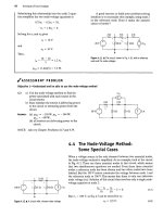
In Chapters 14 and 15, we discovered that an important char-
acteristic of bandpass and bandreject filters is the quality fac-
tor, Q. The quality factor provides a measure of how selective
the filter is at its center frequency. For example, a bandpass
fil-
ter with a large value of Q will amplify signals at or near its
center frequency and will attentuate signals at all other
fre-
quencies. On the other hand, a bandreject filter with a small
value of Q will not effectively distinguish between signals at
the center frequency and signals at frequencies quite different
from the center frequency.
In this chapter, we learn that any periodic signal can be
represented as a sum of sinusoids, where the frequencies of the
sinusoids in the sum are comprised of the frequency of the
periodic signal and integer multiples of that frequency. We can
use a periodic signal like a square wave to test the quality fac-
tor of a bandpass or bandreject filter. To do this, we choose a
square wave whose frequency is the same as the center
fre-
quency of a bandpass filter, for example. If the bandpass filter
has a high quality factor, its output will be nearly sinusoidal,
thereby transforming the input square wave into an output
sinusoid.
If the filter has a low quality factor, its output will
still look like a square wave, as the filter is not able to select
from among the sinusoids that make up the input square wave.
We present an example at the end of this chapter.
h
A
fi
AAA
VIMy
IAAAAA/
1
uvuVuu
High-(?
Bandpass
Filter
A
A
\J
V
605