Electric Circuits, 9th Edition P20 docx
Bạn đang xem bản rút gọn của tài liệu. Xem và tải ngay bản đầy đủ của tài liệu tại đây (789.12 KB, 10 trang )
166
The
Operational Amplifier
Figure
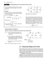
P5.7
Figure
P5.10
10
kfl
AAV
Section
5.3
DESIGN
PROBLEM
5.8 a)
Design
an
inverting amplifier using
an
ideal
op
amp that
has a
gain
of 3. Use a set of
identical
resistors from Appendix
H.
b)
If you
wish
to
amplify
a 5 V
input signal using
the circuit
you
designed
in
part
(a),
what
are the
smallest power supply signals
you can
use?
5.9 The op amp in the
circuit
in Fig. P5.9 is
ideal.
MULTISIM
a
) ^ind the
range
of
values
for a in
which
the op
amp does
not
saturate.
b) Find
i
()
(in
microamperes) when
a =
0.272.
Figure
P5.9
12
kfl
a50
kfl
1.6 kfl
-AAWW-
50
kn
6
250 rnV
6.4 kfl
t
t
l?n
i
io
kn
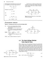
5.10
a) The op amp in the
circuit shown
in Fig. P5.10 is
PSPICE
ideal.
The
adjustable resistor
R± has a
maxi-
mum value
of 100 kfl, and a is
restricted
to the
range
of 0.2 < a < 1.
Calculate
the
range
of
v
n
if v
s
= 40 mV.
b)
If a is not
restricted,
at
what value
of a
will
the
op
amp
saturate?
10
kfl
Section
5.4
5.11 Refer
to the
circuit
in Fig. 5.12,
where
the op amp
PSPICE
is
assumed
to be
ideal. Given that
R
a
= 4 kfl,
.ULTISIM
Rh =
5klli
^
=
2Qka
^
VA S
200 mV,
v
b
= 150 mV, v
c
= 400 mV, and V
cc
= ±6 V,
spec-
ify
the
range
of Rf for
which
the op amp
operates
within
its
linear region.
5.12
The op amp in Fig. P5.12 is
ideal.
PSPICE
a
)
what circuit configuration
is
shown
in
this figure?
b) Find
v
Q
if
4
V.
=
IV, v
h
= 1.5 V, and
c)
The
voltages
v
a
and v
c
remain
at 1 V and -4 V,
respectively. What
are the
limits
on v
b
if the op
amp operates within
its
linear region?
Figure
P5.12
44
kfl
•
VA,
+ 27.5
kfl
220
kfl
AAA-
0
a
•
W^
+
80 kfl
v
h
v„
53.3
kfl
5.13 Design
an
inverting-summing amplifier
so
that
v
a
= -(3¾ + 5v
h
+ 4¾ + 2v
d
).
DE5IGN
PROBLEM
MULTISIM
Start
by
choosing
a
feedback resistor
(Rf)
from
Appendix
H.
Then choose single resistors from
Appendix
H or
construct resistor neworks from resis-
tors
in
Appendix
H to
satisfy
the
design values
for
/?
a
,
/?
b
,
R
c
, and i?
d
.
Draw your final circuit diagram.
Problems
167
5.14
a) The op amp in Fig. P5.14 is
ideal. Find
v
a
if
PSPICE
?
;
a
= 4 V, v
b
= 9 V, v
c
= \3 V, and v
d
= 8 V.
4ULTISIM
b) Assume
v.
A
v
c
, and
v
L
\ retain their values
as
given
in
(a).
Specify
the
range
of v.
x
such that
the op
amp operates within
its
linear region.
Figure
P5.17
Figure
P5.14
40
kil
•
VvV
+ 22kft
•
VW
220
kil
'VW
ii,
T T
Okil
PSPICE
MULTISIM
5.15 Tlie
220 kil
feedback resistor
in the
circuit
in
Fig.
P5.14 is
replaced
by a
variable resistor
Rf. The
voltages
v.
d
- v
d
have
the
same values
as
given
in
Problem 5.14(a).
a) What value
of Rf
will cause
the op amp to
satu-
rate? Note that
0 < R
f
< oo.
b) When
Rf has the
value found
in (a),
what
is the
current
(in
microamperes) into
the
output ter-
minal
of the op
amp?
Section
5.5
5.16
The op amp in the
circuit
of
Fig.
P5.16 is
ideal.
PSPICE
a
\
-yvhat
0
p
am
p
circuit configuration
is
this?
MULTISIM
b) Calculate
v
u
.
Figure
P5.16
40
kH
—A/VV
80
kil
-A<W
5.17
The op amp in the
circuit
of
Fig.
P5.17 is
ideal.
a) What
op amp
circuit configuration
is
this?
b) Find
v
a
in
terms
of v
s
.
c) Find
the
range
of
values
for v
s
such that
v
n
does
not saturate
and the op amp
remains
in its
linear
region
of
operation.
28
kO
5.18
The op amp in the
circuit shown
in
Fig. P5.18
is
ideal.
PSPI
"
a)
Calculate
v
a
when
v.,
equals
4 V.
MULTISIM
' " ."
n
b) Specify
the
range
of
values
of v
s
so
that
the op
amp operates
in a
linear mode.
c) Assume that
v„
equals
2 V and
that
the 63 kil
resistor
is
replaced with
a
variable resistor. What
value
of the
variable resistor will cause
the op
amp
to
saturate?
Figure
P5.18
63
kil
AAA-
i.'„527kn
5.19
a)
Design
a
non-inverting amplifier with
a
gain
of
4.
Use
resistors from Appendix
H. You
might
need
to
combine resistors
in
series
and in
par-
allel
to get the
desired resistance. Draw your
final circuit,
b)
If you use ±
12
V
power supplies
for the op amp,
what range
of
input values will allow
the op amp
to stay
in its
linear operating region?
5.20
The op amp in the
circuit
of
Fig. P5.20
is
ideal.
PSPICE
MULTISIM
a) What
op amp
circuit configuration
is
this?
b) Find
v
<y
in
terms
of v
s
.
c) Find
the
range
of
values
for v
s
such that
v
a
does
not saturate
and the op amp
remains
in its
linear
region
of
operation.
Figure P5.20
60
kil
AA/V-
168 The Operational Amplifier
5.21 The op amp in the circuit shown in Fig. P5.21 is
PSPICE
ideal. The signal voltages v and v
b
are 800 mV and
MULTISIM .„., .,
400 mv, respectively.
a) What circuit configuration is shown in the figure?
b) Calculate v
a
in volts.
c) Find /
a
and /
b
in microamperes.
d) What are the weighting factors associated with
v
a
and v
b
?
Figure P5.21
110
kO
'VW
»„£47kft
T T
5.22 The circuit in Fig. P5.22 is a noninverting summing
PROBLEM amplifier. Assume the op amp is ideal. Design the
PSPICE circuit so that
MULTISIM
v
<>
= y
a + 2«^ + 3v
c
.
a) Specify the numerical values of R
a
and R
c
.
b) Calculate /
a
, /
b
, and /
c
(in microamperes) when
v
a
= 0.7 V, v
b
= 0.4 V, and u
c
= 1.1 V.
Figure P5.22
loo kn
5.23 The op amp in the noninverting summing amplifier
of Fig. P5.23 is ideal.
a) Specify the values of Rf, R
b
, and R
c
so that
v
0
= 6v.
A
+ 3v
h
+ 4v
c
.
PSPICE
MULTISIM
b) Using the values found in part (a) for R
(
, R
h
, and
JR
C
, find (in microamperes) i
a
, /
b
, i
c
, L, and /
s
when
v.
a
= 0.5 V, % = 2.5 V, and v
c
= 1 V.
Figure P5.23
«3.3 kO
Section 5.6
5.24 a) Use the principle of superposition to derive
Eq. 5.22.
b) Derive Eqs. 5.23 and 5.24.
5.25 The resistors in the difference amplifier shown
PSPICE in Fig. 5.15 are K
a
= 24kO, R
b
= 75 kll,
MULTISIM
Rc = 130ka and
^ - 120 kH. The signal volt-
ages v.
d
and v
b
are 8 and 5 V, respectively, and
V
cc
= ±20 V.
a) Find v
(>
.
b) What is the resistance seen by the signal
source y
a
?
c) What is the resistance seen by the signal
source v
b
?
5.26 The op amp in the circuit of Fig. P5.26 is ideal. What
value of R
{
will give the equation
v
()
= 5 - 4v
u
,
for this circuit?
Figure P5.26
Problems
169
DESIGN
PROBLEM
PSPICE
MULTISIM
5.27 Design the difference-amplifier circuit in Fig. P5.27
so that v
(l
= 10(¾¾ - v
a
), and the voltage source v
b
sees an input resistance of 220 kfi. Specify the val-
ues of R
a
,Rb»
and R
t
using single resistors or com-
binations of resistors from Appendix H. Use the
ideal model for the op amp.
Figure P5.27
4.7 kft
DESIGN
PROBLEM
PSPrCE
MULTISIM
5.30 Design a difference amplifier (Fig. 5.15) to meet
the following criteria: v
()
= 3t>
b
—
4i>
a
. The resist-
ance seen by the signal source v
b
is 470 kft, and
the resistance seen by the signal source v.
d
is
22 kft when the output voltage v
()
is zero. Specify
the values of R
a
, R
b
, R
c
, and R
d
using single
resistors or combinations of resistors from
Appendix H.
5.31
»'„$22
kft
5.28 The op amp in the adder-subtracter circuit shown in
PSPICE pig. P5.28 is ideal.
MULTISIM
a) Find v
0
when v
a
= 1 V, v
b
= 2 V, v
c
= 3 V, and
V
d
= 4 V.
b) If v
a
, v
b
, and v
d
are held constant, what values of
v
c
will not saturate the op amp?
The resistor R
£
in the circuit in Fig. P5.31 is
adjusted until the ideal op amp saturates. Specify
R
t
in kilohms.
Figure P5.31
1.6 kO
18 V
5.6 kH
Figure P5.28
20
kft
V W
W/
180
kH
^vw-
<v
18
kft
-AW
30 kO
v
B
147 kfi
20 kH
5.29 Select the values of R
a
and R{ in the circuit in
DESIGN Fig. P5.29 so that
PROBLEM
°
PSPICE
MULTISIM
5.32 The op amp in the circuit of Fig. P5.32 is ideal.
a) Plot v„ versus a when Rf =
4R-[
and v
g
=* 2 V.
Use increments of 0.1 and note by hypothesis
thatO < a < 1.0.
b) Write an equation for the straight line you plot-
ted in (a). How are the slope and inter-
cept of the line related to v
g
and the ratio Rf/Ri?
c) Using the results from (b), choose values for v
g
and the ratio Rf/R\ such that v
a
= -6a + 4.
Figure P5.32
v
a
= 5000(;
b
- Q.
Use single resistors or combinations of resistors
from Appendix H.The op amp is ideal.
Figure P5.29
»«t*L
t)
%**
170 The Operational Amplifier
5.33 In the difference amplifier shown in Fig.
P5.33,
what
range of values of R
x
yields a CMRR > 1000?
Figure P5.33
50kil
'WW
5.34 In the difference amplifier shown in Fig. P5.34,
compute (a) the differential mode gain, (b) the
common mode gain, and (c) the CMRR.
Figure
P5.34
1 kO
^L
<b x
i
vJ
[
Y
i
ikn
) <
i
25kfl
r^f 10V
^"S-iov
124 kO
1
+
»„
r
Sections 5.1-5.6
5.35 Assume that the ideal op amp in the circuit seen in
Fig. P5.35 is operating in its linear region.
a) Show that v
0
= [(/?, + R
2
)/R
x
\v
s
.
b) What happens if R
1
—•
oo and R
2
-» 0?
c) Explain why this circuit is referred to as a volt-
age follower when Z?j = oo and R
2
= 0.
Figure P5.35
5.36 The voltage v
g
shown in Fig. P5.36(a) is applied to
PSPICE
tne
inverting amplifier shown in Fig. P5.36(b).
1ULTISIM <-,,,, ,, 11
Sketch v„ versus f, assuming the op amp is ideal.
Figure P5.36
v
0.5
V
-0.5 V
(a)
120
kO
7.5 kO
—AMs
•o
"»%6.8ka
(b)
5.37 Tlie signal voltage v
g
in the circuit shown in
Fig.
P5.37
PSPICE
j
s
described by the following equations:
MULTISIM *•
v
e
= 0,
0,
v
g
= 10 sin(ir/3)/ V, 0 < / < oo.
Sketch v
a
versus r, assuming the op amp is ideal.
Figure P5.37
15
kO
75 kH
»,,
f 6.8 kfi
5.38 a) Show that when the ideal op amp in Fig. P5.38 is
operating in its linear region,
.
3V
8
*•
=
-R-
b) Show that the ideal op amp will saturate when
R(±V
CC
~ 2v
g
)
R*
=
3v
g
Problems
171
Figure P5.38
5.39 Assume that
the
ideal
op amp in the
circuit
in
PSPICE
Fig.
P5.39
is
operating
in
its
linear region.
MULTISIM
a) Calculate
the
power delivered
to the
16
kO
resistor.
b) Repeat
(a)
with
the op
amp
removed from
the
circuit, that is, with
the 16
kfit resistor connected
in
the
series with
the
voltage source
and the
48
kft
resistor.
c) Find
the
ratio
of
the
power found
in (a) to
that
found
in
(b).
d) Does
the
insertion
of the op
amp
between
the
source
and the
load serve
a
useful purpose?
Explain.
Figure P5.39
320
mV
5.40 The circuit inside
the
shaded area
in
Fig.
P5.40
is
a
con-
PSPICE
s
tant current source
for
a
limited range
of
values
of
R
f
.
MULTISIM
a) Find
the
value
of i
L
for R
L
= 4 kft.
b) Find
the
maximum value
for R
L
for
which
i
L
will
have
the
value
in
(a).
c) Assume that
R
L
=
16 kft.
Explain
the
operation
of
the
circuit.
You
can
assume that
i
n
= i
p
~ 0
under
all
operating conditions.
d) Sketch
i
L
versus
R
L
for 0 < R
L
<
16
kft.
Figure P5.40
50
kfl
'v©
,.
-20V
[
IA
R
L
(
t
Jh
l
t-\:
:4 left
5.41
The two op
amps
in the
circuit
in
Fig. P5.41
are
PSPICE
ideal. Calculate v„\ and v
o2
.
MULTISIM
Figure
P5.41
15
V
15
V
10 V
«4,2 f5kft
5.42
The
op
amps
in
the
circuit
in
Fig. P5.42
are
ideal.
PSPICE
a)
Find/
a
.
ULTISIM
b) Find
the
value
of the
left source voltage
for
which
/
n
= 0.
Figure P5.42
10
kn
i—vvv—4
47
kD
-vw
220
kH
AAA-
IV
©
33
kH
AA/v—i
6
150
mV
172 The Operational Amplifier
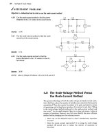
Section 5.7
5.43 Repeat Assessment Problem 5.6, given that the
PSPICE inverting amplifier is loaded with a 500 ft resistor.
MULTISIM
5.44 Assume the input resistance of the op amp in
PSPKE
Fig. P5.44 is infinite and its output resistance is zero.
MULTISIM
a) Find v
0
as a function of v
g
and the open-loop
gain A.
b) What is the value of v
0
if v
g
- 1 V and A = 150?
c) What is the value of v
0
if v
g
= 1 V and A - oo?
d) How large does A have to be so that v
{)
is 99% of
its value in (c)?
Figure P5.44
10
kfl
'VW-
5.46
PSPICE
MULTISIM
a) Find the Thevenin equivalent circuit with
respect to the output terminals a,b for the
inverting amplifier of Fig. P5.46. The dc signal
source has a value of 880 mV. The op amp has
an input resistance of 500 kft, an output
resistance of 2 kft and an open-loop gain
of 100,000.
b) What is the output resistance of the inverting
amplifier?
c) What is the resistance (in ohms) seen by the sig-
nal source v
s
when the load at the terminals a,b
is 330 ft?
Figure P5.46
24 kO
AW-
5.45 The op amp in the noninverting amplifier circuit of
PSPICE Fig. P5.45 has an input resistance of 560 kft, an out-
WLTISIM p
Ut res
{
s
t
ance 0
f § kO, and an open-loop gain of
50,000. Assume that the op amp is operating in its
linear region.
a) Calculate the voltage gain
(v
()
/v
g
).
b) Find the inverting and noninverting input volt-
ages v
n
and v
p
(in millivolts) if v
g
— 1 V.
c) Calculate the difference (v
p
- v
n
) in microvolts
when
Vg
~ 1 V.
d) Find the current drain in picoamperes on the
signal source v
R
when v
g
= 1 V.
e) Repeat (a)-(d) assuming an ideal op amp.
5.47 Repeat Problem 5.46 assuming an ideal op amp.
Figure P5.45
200
kft
20
kCL
PSPICE
MULTISIM
5.48 Derive Eq. 5.60.
Sections 5.1-5.7
5.49 Suppose the strain gages in the bridge in Fig. 5.21
PRACTICAL have the value 120 ft ± 1%. The power supplies
PERSPECTIVE
r r r
to the op amp are ±15V, and the refer-
ence voltage, v
rc{
, is taken from the positive
power supply.
a) Calculate the value of Rf so that when the strain
gage that is lengthening reaches its maximum
length, the output voltage is 5 V.
b) Suppose that we can accurately measure
50 mV changes in the output voltage. What
change in strain gage resistance can be
detected in milliohms?
Problems 173
5.50
PRACTICAL
PERSPECTIVE
a) For the circuit shown in Fig. P5.50, show that if
AR « R, the output voltage of the op amp is
approximately
show that the percent error in the approxima-
tion of
v„
in Problem 5.50 is
R
2
(R + 2R
t
)
(~AR)v
h
AR (R + Re)
%
error
= — 7½
TTTT
X 100.
R (R + 2R
{
)
b) Find v
()
if R
f
= 470 kfl, R = 10 kf>, AR = 95 ft,
and v
in
= 15 V.
c) Find the actual value of v
a
in (b).
Figure P5.50
5.51 a) If percent error is defined as
PRAOICAL
PERSPECTIVE
PSPICE
MULTISIM
% error =
approximate value
true value
- 1 x 100,
b) Calculate the percent error in v
a
for Problem 5.50.
5.52 Assume the percent error in the approximation of
PRACTICAL v
t)
in the circuit in Fig. P5.50 is not to exceed 1%.
PERSPECTIVE " °
PSPICE What is the largest percent change in R that can be
MULTisiM tolerated?
5.53 Assume the resistor in the variable branch of the
PRACTICAL bridge circuit in Fig. P5.50 is R
PERSPECTIVE
n
°
L
°
R + AR.
AR instead of
PSPICE
MULTISIM
a) What is the expression for v
()
if AR « R?
b) What is the expression for the percent error in
v
a
as a function of R, i?
f
, and AR1
c) Assume the resistance in the variable arm of
the bridge circuit in Fig. P5.50 is 9810 fi and the
values of R, R
(
, and v
m
are the same as in
Problem 5.50(b). What is the approximate value
of
v
a
'?
d) What is the percent error in the approximation
of v
(}
when the variable arm resistance is
9810 a?
• t _•< aBniri
r
6.1 The Inductor p. 176
6.2 The Capacitor p. 182
6.3 Series-Parallel Combinations of Inductance
and Capacitance p. 187
6.4 Mutual Inductance p. 189
6.5 A Closer Look at Mutual Inductance p. 193
1 Know and be able to use the equations for
voltage, current, power, and energy in an
inductor; understand how an inductor behaves
in the presence of constant current, and the
requirement that the current be continuous in
an inductor.
2 Know and be able to use the equations for
voltage, current, power, and energy in a
capacitor; understand how a capacitor behaves
in the presence of constant voltage, and the
requirement that the voltage be continuous in a
capacitor.
3 Be able to combine inductors with initial
conditions in series and in parallel to form a
single equivalent inductor with an initial
condition;
be able to combine capacitors with
initial conditions in series and in parallel to
form a single equivalent capacitor with an
initial condition.
4 Understand the basic concept of mutual
inductance and be able to write mesh-current
equations for a circuit containing magnetically
coupled coils using the dot convention
correctly.
174
Inductance, Capacitance,
and Mutual Inductance
We begin this chapter by introducing the last two ideal circuit
elements mentioned in Chapter 2, namely, inductors and capaci-
tors.
Be assured that the circuit analysis techniques introduced in
Chapters
3
and
4
apply to circuits containing inductors and capac-
itors.
Therefore, once you understand the terminal behavior of
these elements in terms of current and voltage, you can use
Kirchhoff s laws to describe any interconnections with the other
basic elements. Like other components, inductors and capacitors
are easier to describe in terms of circuit variables rather than
electromagnetic field variables. However, before we focus on the
circuit descriptions, a brief review of the field concepts under-
lying these basic elements is in order.
An inductor is an electrical component that opposes any
change in electrical current. It is composed of a coil of wire
wound around a supporting core whose material may be mag-
netic or nonmagnetic. The behavior of inductors is based on phe-
nomena associated with magnetic fields. The source of the
magnetic field is charge in motion, or current. If the current is
varying with time, the magnetic field is varying with
time.
A time-
varying magnetic field induces a voltage in any conductor linked
by the field. The circuit parameter of inductance relates the
induced voltage to the current. We discuss this quantitative rela-
tionship in Section 6.1.
A capacitor is an electrical component that consists of two
conductors separated by an insulator or dielectric material. The
capacitor is the only device other than a battery that can store
electrical
charge.
The behavior of capacitors is based on phenom-
ena associated with electric fields. The source of the electric field
is separation of charge, or voltage. If the voltage is varying with
time,
the electric field is varying with
time.
A time-varying electric
field produces a displacement current in the space occupied by
the field. The circuit parameter of capacitance relates the dis-
placement current to the voltage, where the displacement current
is equal to the conduction current at the terminals of the capaci-
tor. We discuss this quantitative relationship in Section 6.2.
Practical Perspective
Proximity Switches
The electrical devices we use in our daily lives contain many
switches. Most switches are mechanical, such as the one used
in the flashlight introduced in Chapter 2. Mechanical switches
use an actuator that is pushed, pulled,
slid,
or rotated, caus-
ing two pieces of conducting metal to touch and create a
short circuit. Sometimes designers prefer to use switches
without moving parts, to increase the safety, reliability,
con-
venience, or novelty of their products. Such switches are
called proximity switches. Proximity switches can employ a
variety of sensor technologies. For example, some elevator
doors stay open whenever a light beam is obstructed.
Another sensor technology used in proximity switches
detects people by responding to the disruption they cause in
electric fields. This type of proximity switch is used in some
desk lamps that turn on and off when touched and in elevator
buttons with no moving parts (as shown in the figure). The
switch is based on a capacitor. As you are about to discover in
this chapter, a capacitor is a circuit element whose terminal
characteristics are determined by electric fields. When you
touch a capacitive proximity switch, you produce a change in
the value of
a
capacitor, causing a voltage change, which
acti-
vates the switch. The design of a capacitive touch-sensitive
switch is the topic of the Practical Perspective example at the
end of this chapter.
175