- Trang chủ >>
- Khoa Học Tự Nhiên >>
- Vật lý
Handbook of algorithms for physical design automation part 7 ppsx
Bạn đang xem bản rút gọn của tài liệu. Xem và tải ngay bản đầy đủ của tài liệu tại đây (178.5 KB, 10 trang )
Alpert/Handbook of Algorithms for Physical Design Automation AU7242_C003 Finals Page 42 29-9-2008 #15
42 Handbook of Algorithms for Physical Design Automation
3.2 NOISE
Coupling noise is yet another unwanted side effect of the scaling in deep submicron technology,
and its impact can be reduced through physical design transformations. The effect arises due to
geometric scaling, which requires the wires to be narrower and the spacing between adjacent wires
smaller. On the other hand, because the chip size is also getting larger (in terms of multiples o f the
minimum feature size), it is necessary to reduce wire resistance b y increasing the aspect ratio of
the wire cross section. The compounded effect is the increase of the coupling capacitance between
adjacent signal wires.
When two interconnect networks are capacitively coupled, usually the one with the stronger
driving gate is referred to as the aggressor, while the one with the weaker driver is called the victim.
It is quite possible that an aggressor can affect multiple victims, and a victim can have more than
one aggressors. For simplicity, we only discuss the case with one aggressor and one victim. These
ideas can be easily extended to more general cases. The application domain for this analysis is in
noise-aware routing. For scalable methods that can be applied to full-chip noise analysis, the reader
is referred to Chapter 34.
When the aggressor switches, if the victim is quiet, then the coupling will generate a glitch on
the victim wire. If the glitch is sufficiently large and occurs within a certain timing window, the
(erron eous) glitch can be latche d into a memory storage elem ent and cause a logic error. If th e victim
is also switching, then depending on the polarities of the signals and the corresponding switching
windows, the signal on the victim wire can be slowed down or sped up, which may cause timing
violations. Although very elaborate algorithms are available to estimate the couplingeffects between
the signal wires, (see Refs. [9,10]), it is highly desirable to correct the problem at its root, i.e., during
the physical design phase.
The exact amount of noise injected to the victim net from the aggressor is a function of circuit
topologies and values of both aggressor and victim nets, as well as the properties of the signal. To
accurately estimate the noise, every component of the coupled network is required, which is not
realistic during physical design. Fortunately, there is a simple noise metric equivalent to Elmore
delay in timing [11].
In Ref. [11], it is assumed that the excitations in the aggressor net are infinite ramps, which are
signals whose first derivativesare zero beforet = 0, and constant afterward. Fromthe circuit analysis
point of view, the coupling capacitors act like differentiators. Thus, the coupling node voltage will
come to a steady state, whose level can be used as an indicator of the coupling effect. For a circuit of
general topology, the noise metric must be solved with circuit analysis techniques, which involves
the construction o f MNA formulations and solving of the matrices. The MNA matrices of a coupled
circuit can be written as
G
11
0
0G
22
x
1
x
2
+
C
11
C
c
C
T
c
C
22
˙x
1
˙x
2
=
B
1
0
u
In the above equation, the first partition is the aggressor net while the second partition is the victim
net. The submatrices G
11
and C
11
represent the conductance and capacitance of the aggressor net;
and G
22
and C
22
represent the conductances and capacitances of the victim net; while C
c
represents
the coupling between the two nets. According to Ref. [11], simple algebraic manipulations can be
employed to estimate the worst case as
V
2,max
= G
−1
22
C
c
G
−1
11
B
1
˙u
Note that the worst-case noise is only a function of the resistances of the victim an d aggressor nets, as
well as the coupling capacitances. It is not a function of the self-capacitances of the two nets (under
the assumption that the input is an infinite ramp).
Alpert/Handbook of Algorithms for Physical Design Automation AU7242_C003 Finals Page 43 29-9-2008 #16
Metrics Used in Physical Design 43
If both aggressor and victim nets have tree-like topologies, then the above noise metric can be
calculated with a simple graph traversal, which is similar to the Elmore delay calculation of tree-like
RC networks. To illustrate the p rocedure, we can rewrite the worst-case noise metric as
I
c
= C
c
G
−1
11
B
1
˙u
V
2,max
= G
−1
22
I
c
(3.10)
Because the excitation in the aggressor net is an infinite ramp, the term I
c
represents the coupling
current injected in to the victim net. If the aggressor net is properly connected, then it can be shown
using simple circuit arguments [11] that the injected current is simply C
c
˙u. The calculation of the
voltage inthe victim netcan then becarried out usinga proceduresimilar to Elmore delaypropagation,
except that we traverse the tree from the root to the leaf nodes. To illustrate the procedure, we give
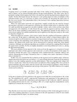
a simple example shown in Figure 3.7.
Because the noise is not a function of the self-capacitance of either the aggressor or the victim,
it is not drawnin the diagram. Inthe first step of the calculation,the equivalentcurrent injections from
the aggressor net is calculated, which correspond to evaluating the first equation in Equation3.10.
Because there is no direct resistive path to ground and there is only one independent voltage source
in the aggressor, it is trivial to show that
I
1
= C
1
·˙u
I
2
= C
2
·˙u
I
3
= C
3
·˙u
We then replace the coupling capacitors of the victim with those current sources. Because the root
of the tree is grounded, we calculate the worst-case noise by a graph traversal, from root to leaves:
I
B,max
= R
1
(C
1
+ C
2
+ C
3
)˙u
I
D,max
= R
1
(C
1
+ C
2
+ C
3
)˙u + R
2
(C
2
+ C
3
)˙u
I
E,max
= R
1
(C
1
+ C
2
+ C
3
)˙u + R
2
(C
2
+ C
3
)˙u + R
3
(C
3
)˙u
I
F,max
= R
1
(C
1
+ C
2
+ C
3
)˙u + R
2
(C
2
+ C
3
)˙u
Although Devgan’s metric is easy to calculate, its accuracy is limited. For fast transitions, in par-
ticular, the metric evaluates to a physically impossible value that exceeds the supply voltage. Note
that the evaluation is still correct, as Devgan’s noise metric only guarantees an upper bound on the
noise; however, the accuracy in such cases is clearly limited.
To improve accuracy, a further improvementof the static noise metric was proposed in Ref. [12],
which extended the idea of Devgan’s metric through the use of more than one moment. In addition,
R
1
R
3
R
R
2
F
E
DB
C
1
C
2
C
3
Victim
Aggressor
R
1
R
3
R
R
2
F
E
DB
Victim
I
1
I
2
I
3
(a) (b)
FIGURE 3.7 An example of worst-case noise cal culation, showing (a) the original c ircuit and(b) the equivalent
circuit when coupling capacitors are replaced by injected noise current sources. (From Sapatnekar, S. S., Timing,
Kluwer Academic Publisher, Boston, MA, 2004. With permission.)
Alpert/Handbook of Algorithms for Physical Design Automation AU7242_C003 Finals Page 44 29-9-2008 #17
44 Handbook of Algorithms for Physical Design Automation
C
1
0
R
1
C
2
R
2
C
c
V
VictimAggressor
FIGURE 3.8 Circuit diagram for the derivation of the transient noise peak.
the aggressor excitation was assumed to be a first-order exponential function rather than an infinite
ramp. To obtain a closed-form noise metric, the response at the victim net was calculated using
moment-matching approach.
Another type of noise metric that takes the transient approach is the work in Ref. [13]. Instead
of assuming that the excitation at the aggressor is an infinite ramp, it is assumed that the aggressor
excitation is a step signal. However, the circuit topology is highly simplified so that a close-form noise
metric can be derived. The aggressor–victim pair is simplified as shown in Figure 3.8 [13], where R
1
is the total resistance of the aggressor and R
2
is the total resistance of the victim. Note that the victim
is grounded by a zero-valued voltage source. It then can be proved that the noise peak at node V is
X
V
=
1
1 +
C
2
C
c
+
R
1
R
2
1 +
C
1
C
c
An alternative two-stage π model is presented in the metric in Ref. [14].
For long global nets, there is also the possibility that two nets are inductively coupled, especially
when the the aggressor and victim nets are in parallel, such as in a bus structure. The analysis and
estimation of the inductively coupling is much more involved. Because inductive coupling m ostly
occurs in selected cases, quite often detailed circu it analysis is affordable. In many cases, various
types of shielding are implemented to minimize the inductive coupling effect [15,16].
3.3 POWER
With the decreasing transistor channellengths and increasingdie sizes, powerdissipation has become
a major design constraint. There are three major components of power dissipation: the dynamic
power, the short-circuit power, and the static power. Historically, the dynamic power and short-
circuit power have been the subject of many studies. In recent years, as the complimentary metal
oxide semiconductor (CMOS) devices rapidly approach the fundamental scaling limit, static power
has become a major component of the total power consumption. We discuss these components
separately in the subsequent subsections.
3.3.1 DYNAMIC POWER
For a CMOS circuit, its states are represented by the charges stored at various metal oxide semicon-
ductor field effect transistors (MOSFETs). When the circuit is operating, the change of the circuit
states is realized by charging and discharging of these transistors. This charge/discharge operation
can be illustrated in the simple circuit shown in Figure 3.9. When the circuit is in quiescence, inverter s
INV1, INV2, and INV3 store 1, 0, and 1, respectively. When a falling transition occurs at the input
Alpert/Handbook of Algorithms for Physical Design Automation AU7242_C003 Finals Page 45 29-9-2008 #18
Metrics Used in Physical Design 45
M1
M2
M3
M4
M5
M6
INV1 INV2 INV3
FIGURE 3.9 A simple circuit to illustrate charging and discharging of the gate capacitors.
of INV1, the state of INV2 changes from 0 to 1, by charging the gate capacitor of MOSFET M3 and
M4 via transistor M1. In the meantime, the state of INV3 changes from 1 to 0, which is achieved by
discharging the gate capacitor of M5 and M6 to ground (via M4).
Consider gate INV1, whose output is being charged from low to high. During this transition, the
output parasitic capacitance is charged, and some energy is dissipated in the (nonlinear) positive-
channel metal oxide semiconductor (PMOS) transistor resistance. It can be shown that for a single
transition, each of these components equals
1
2
C
L
V
2
DD
,whereC
L
is the load capacitance at the output,
and this energy is supplied by the V
DD
source. In a subsequent cycle, when the output of INV1
discharges, all of the dynamic energy dissipated in the negative-channel metal oxide semiconductor
(NMOS) transistor comes from the capacitor C
L
, and none comes from V
DD
. Therefore, for every
high-to-low-to-high transition, the energy dissipated in a single cycle can be calculated as
P
dynamic
= C
gate
V
2
DD
(3.11)
where C
gate
is th e total capacitance of all gate capacitors involved. If a rising transition occurs next,
the energy stored at the gate capacitance of M3 and M4 is simply dissipated to ground.
This concept can be generalized from inverters to arbitrary gates, and the essential idea and the
formula remain valid. If the clock frequency is f and the gate switches on every clock transition,
then the number of transitions is multiplied by f . The power dissipated can then be calculated as
the energy dissipated per unit time. In general, though, a gate does not switch on every single clock
transition, and if α is the p robability that a gate will switch during a clock transition, the dynamic
power of the gate can be estimated as
P
dynamic
= αC
gate
V
2
DD
f (3.12)
Here, α is referred to as the switching factor for the gate.
The total power of the circuit can be computed by summing up Equation3.12 over all gates in
the circuit. For a circuit in which the final signal value settles to V
DD
,asisthecaseforstaticCMOS
logic, the above calculation is accurate; simple extensions are available for other logic circuits (such
as pass transistor logic) where the signal value does not reach V
DD
[17].
The value of α is dependent on the context of the gate in the circuit. For tree-like structures, this
computation is straightforward, but for general circuits with reconvergent fanout, it is quite difficult
to accurately calculate the switching factors [18]. Nevertheless, numerous heuristic approaches are
available, and are widely used.
From the physical design point of view, usually the supply voltage V
DD
is determined by the
technology and the switching factor α is determined by the logic synthesis. Therefore, only gate
capacitance C
gate
can beoptimizedduring thephysicaloptimizationphase.As shownin Equation3.12,
the smaller the overall gate capacitance, the smaller the dynamic power. The minimization of the
overall gate size (while maintaining the necessary timing constraints) is actually the same objective
Alpert/Handbook of Algorithms for Physical Design Automation AU7242_C003 Finals Page 46 29-9-2008 #19
46 Handbook of Algorithms for Physical Design Automation
of many physical design algorithms. Therefore, an optimal solution of those algorithms is also the
optimal solution in terms of dynamic power.
Another approach to reduce dynamic power is to avoid unnecessary toggling of the devices. This
is possible for state-storage devices such as latches and flip-flops. A carefully designed clock gating
scheme can greatly reduce dynamic power. However, usually these techniques are beyond the scope
of physical design flows.
3.3.2 SHORT-CIRCUIT POWER
The mechanism of short-current power can be illustrated in the simple example shown in Figure 3.9.
For INV1, when the falling transition occurs at the input, the PMOS device M1 switches from o ff
to on, while the NMOS device M2 switches from on to off. Because of the intrinsic delays of the
MOSFET devices as well as the loading effect of the gate capacitance of INV2, the switching cannot
occur instantaneously. For a short period during the transition, both M1 and M2 are partially on,
thus providing a direct path between the power supply and the ground. Certain amount of power is
dissipated by this short-circuit current, which is also referred as the shoot-through current.
The short-circuit power has strong dependence o n the capacitive load and the input signal tran-
sition time. Although accurate circuit simulation can be applied to calculate the short-circuit power,
such an approach is prohibitively expensive. A more realistic approach is to estimate the short-circuit
power via empirical equations. Some analysis techniques are proposed in Refs. [19,20]. However,
according to many reports, the short-circuit current only accounts for between 5 and 10 percent of
total power consumption in a well-designed circuit.
3.3.3 STATIC POWER
In a digital circuit, MOSFET devices function as switches to realize certain logic functions. Ideally,
we would like these switches to be completely off when the the controlling gate is off. However,
MOSFET devices are far from ideal. Even when the circuit is not operating, the MOSFET devices are
“leaking” current between terminals. Although each transistor only leaks a small amount of current,
the overall full chip leakage can be substantial due to the sheer number of transistors.
There are two major components of leakage current: subthreshold leakage current and gate tun-
neling current [21]. These two components are illustrated in Figure 3.10. The subthreshold leakage
current (I
1
in Figure 3.10) is the leakage current between the drain and source node when the device
is in the off state (the voltage between the gate and source terminal is zero). Historically, in 0.25 µm
and h igher technology nodes, the subthreshold leakage was small enough to be negligible (several
orders of magnitudesmaller than the on-current). However,the traditional scaling requires the reduc-
tion of supply voltage V
DD
, along with the reduction of the channel length. As a consequence, the
threshold voltage must be scaled accordingly to maintain the driving capability of the MOSFET
I
2
I
1
Source
Drain
Gate
FIGURE 3.10 Two major components of the leakage current.
Alpert/Handbook of Algorithms for Physical Design Automation AU7242_C003 Finals Page 47 29-9-2008 #20
Metrics Used in Physical Design 47
device. The smaller threshold voltage causes large increase of subthreshold leakage current, so that
this is a significant factor in nanometer technologies.
The second component of the static power is the gate tunneling current (I
2
in Figure 3.10), which
is also the consequence of scaling. As the device dimensions are reduced, the gate oxide thickness
also has to be reduced. An unwanted consequence of thinner gate oxide thickness is the increased
gate tunneling leakage current.
Many factors can affect the amount of subthreshold leakage current, including many device and
environmental variables. An expression for the subthreshold leakage current density, i.e., the current
per unit transistor area, is given by Ref. [22]:
J
sub
=
W
L
eff
µ
q
si
N
cheff
2φ
s
υ
2
T
exp
V
gs
− V
th
ηυ
T
1 −exp
−V
ds
υ
T
(3.13)
The details of the parameters in the above equation can be found in Ref. [22]. Here we would like to
mention a few points:
• Term υ
T
= kT/q is the ther mal voltage, where k is the Boltzmann’s constant, q is the
electrical charge, and T is the junction temperature. From the equation, we can see that the
leakage is an exponential function of the junction temperature T .
• Symbol V
th
represents the threshold voltage. It can be shown that for a given technology,
V
th
is a function of the effective channel length L
eff
. Therefore, subthreshold leakage is also
an exponential function of effective channel length.
• Drain-to-source voltage, V
ds
, is closely related to supply voltage V
DD
, and has the same
range in static CMOS circuits. Therefore, subthreshold leakage is an exponential function
of the supply voltage.
• Threshold voltage V
th
is also affected by the body bias V
BS
. In a bulk CMOS technology,
because the body node is always tied to ground for NMOS and V
DD
for PMOS, the body bias
conditions for stacked devices are different, depending on the location of the off device on
a stack (e.g., top of the stack or bottom of the stack). As a result, the subthreshold leakage
current can quite vary when different input vectors are applied to a gate with stacks.
For the gate tunneling current, a widely used model is the one provided in Ref. [23]:
J
tunnel
=
4πm
∗
q
h
3
(kT)
2
1 +
γ kT
2
√
E
B
exp
E
F0,Si/SiO
2
kT
exp
−γ
E
B
(3.14)
where
T is the operating temperature
E
F0,Si/SiO
2
is the Fermi level at the Si/SiO
2
interface
m
∗
depends on the the underlying tunneling mechanism
Parameters k and q are d efined as above, and h is Planck’s constant: all of these are physical
constants. The term γ = 4πt
OX
√
2m
OX
/h,wheret
ox
is the oxide thicknes, and m
ox
is the effective
electron mass in the oxide. Besides physical constants and many technology-dependent parameters,
it is quite clear that the gate-tunnelingleakage depends on the gate oxide thickness and the operating
temperature. The former is a strong dependence, but the latter is more complex: over normal ranges
of operating temperature, the variations in gate leakage are roughly linear. In comparison with sub-
threshold leakage, which shows exponential changes with temperature, these gate leakage variations
are often much lower. More details about this model can be found in Ref. [23].
One possible solution to mitigate the negative impact of gate current is to use material with
higher dielectric constants (so-called high-k material) in junction with metal gates [24]. In many
Alpert/Handbook of Algorithms for Physical Design Automation AU7242_C003 Finals Page 48 29-9-2008 #21
48 Handbook of Algorithms for Physical Design Automation
current technologies, the gate leakage component is non-negligible. Recently, some progress has
been reported on the development of high-k material. If successfully deployed, the new technology
can reduce gate tunneling leakage by at least an order of magnitude, and at least postpone the point
at which gate leakage becomes significant.
Owing to the power consumption limit dictated by the air-cooling technique widely accepted by
the industry and market, power consumption, especially static power, has become a major design
constraint. In addition to the advancements in manufacturing technology and materialscience, several
circuit level power reduction techniques also have implications on the physical design flow. They
include power gating, V
th
(or effective channel length) assignment, input vector assignment, or any
combination of these methods. More details on these topics can be found in Refs. [21,25–27].
3.4 TEMPERATURE
One of the primary effects of increased power dissipation is that it can lead to a higher on-chip
operating temperature. High chip temperature is not onlya performance issue but also areliability and
cost issue. High channel temperatureaffects MOSFET device performanceby reducing the threshold
voltage V
th
and the mobility. If V
DD
is unchanged,the lowered thresholdvoltage usuallyleads to larger
driving cur rent, while reduced mobility leads to smaller driving current. For a normal design with an
increase of 100
◦
C, the effect is dominated by mobility reduction, thus higher temperature leads to
smaller overall driving capability[28], although inverse temperature dependence, where the speedof a
gate increases with temperature,is also seen [29].For interconnectnetworks,higher wire temperature
will causelarger interconnect delay because metalhas positive temperaturecoefficients.For example,
for every 10
◦
C increase, the resistivity of copper will increase by approximately 3 percent. On the
reliability side, at elevated temperature, the metal molecules are more prone to electromigration,
negative temperature bias instability (NBTI) [30–32], and time-depende ntoxide breakdown (TDDB)
[33]. Th us, temperature is always an important factor in reliability analysis. From a cost point of
view, the cost of a heat sinking solution increases steeply with the total power dissipation of the chip.
Air-cooled technologies are the cheapest option, but these can achieve only a certain level of cooling;
beyond this level, all available options are substantially more expensive, and in today’s commercial
world, they are not viable for consumer products.
For many high-performance microprocessors, due to the large size of the die and large power
dissipation, it is common to observe a temperature differential of 30
◦
C–50
◦
C between regions with
high switching activity levels(e.g., aprocessor core) andthose withlow activitylevels(e.g., memory).
Potentially, these large spatial distributions can cause functional failures.
Before describing the flow of thermal analysis, we briefly describe how heat is dissipated from
today’s IC product. Figure 3.11 shows a highly simplified cross section of a typical IC product. Most
Si substrate with active devices
SiO
2
(if SOI)
Si substrate
Heat spreader
Heat sink
PCB
Package
C4
BEOL metal and ILD layers
FIGURE 3.11 Simplified cross section to illustrate heat transfer from an IC chip.
Alpert/Handbook of Algorithms for Physical Design Automation AU7242_C003 Finals Page 49 29-9-2008 #22
Metrics Used in Physical Design 49
high-performance IC designs use C4 technology for I/O and power delivery (versus the cheaper
wire-bond technology that is used for lower performanceparts). Hundreds to thousands of lead C4’s
are placed on top of the metal layer, and are connected to the printed circuit board (PCB) via the
package. On the substrate side, a heat spreader is mounted next to the die, which is connected to
a heat sink. The whole structure actually is “flipped” upside down so that a heat sink is on the top
(thus C4 technology is also called flip-chip technology). The heat can be dissipated from both the
heat sink side and the C4 side. However, because the heat sink has much smaller thermal resistivity,
majority of the heat is dissipated from the heat sink.
There are three major mechanisms for heat transfer: conduction, convection, and radiation [34].
Convection occurs when heat is transferred by fluid movement (e.g., air or water). Radiation is the
mechanism when the heat is transferred by photons of light in the spectrum. For modern IC products,
convectionand radiation onlyo ccur at interface ofthe heat sink, while almost all on-chip heattransfer
is through conduction.The heat transfer at the heat sink interface is often described as a macromodel.
For on-chip thermal analysis, cooling issues related to the heat sink are often decoupledfrom on-chip
analysis by assuming it to be at the ambient temperature. Therefore, we only focus on conduction in
this section.
The fundamental physics law governingheat conductionis the Fourier’s law. If uniform material
is assumed, it can be described as
∇
2
T(r) +
g(r)
k
r
=
ρc
k
r
∂T
∂t
where
k is the thermal conductivity at the particular location
ρ is the density of th e material
c is the specific heat capacity
g is the volume power density, which is also location dependent
Usually the problem is formulated in three-dimensional space, therefore r is a three-dimensional
array r = (x, y, z). Because the time constant of on-chip temperature change is usually in the order
of milliseconds, while the operating frequency of electric signal is in the picoseconds range, it is
often assumed that the thermal dissipation is a steady-state problem. Under this assumption, the heat
diffusion equation can be simplified as
∇
2
T(r) =−
g(r)
k
r
(3.15)
To solve the above three-dimensional thermal equation, appropriate boundary conditions need
to be established. Because many layers of materials are involved and they all have different thermal
conductivities, also due to the fact that power density distribution is uneven across the die, usually
relatively fine spatial discretization is needed. Overall, it is difficult to solve the problem analytically.
Instead a numerical method is applied.
Like other partial differential equations, the heat diffusion problem can be solved using the
finite difference method [35,36], the finite element method, or the boundary element method [37].
A commonly used method is the finite difference method. Because ∇
2
T(r) =
∂
2
T
∂x
2
+
∂
2
T
∂y
2
+
∂
2
T
∂z
2
,ifwe
discretized the space in 3D space, the term
∂
2
T
∂x
2
can be approximated by
∂
2
T
∂x
2
≈
T
i+1, j, k
− 2T
i, j, k
+ T
i−1, j, k
x
2
where i, j,andk are the indexes in the x, y,andt directions, respectively. After some algebraic
manipulation, the steady-state thermal diffusion problem can be formulated into the matrix form:
Alpert/Handbook of Algorithms for Physical Design Automation AU7242_C003 Finals Page 50 29-9-2008 #23
50 Handbook of Algorithms for Physical Design Automation
GT = P
where
G is the thermal conductance matrix
unknown vector T is the steady-state temperature at all mesh points
Depending on the resolution required, the size of the problem can be quite large. The problem
can be solved by applying a direct solver or using iterative techniques [35,38,39].
Like the finite difference method, the finite element method also results in a matrix of the type
KT = P (3.16)
although in this case, the left-hand side coefficient m atrix is denser (but still qualifies as a sparse
matrix). The T variables here are node temperatures in the discretization, and the elements of K
can be set up using element stamps. The finite element method essentially uses a polynomial fit
within each grid cell, and the element stamps represent this fit. In th e finite element parlance, the
left-hand side matrix, K, is referred to as the global stiffness matrix. Stamps for boundary conditions
can similarly be derived. Conductive boundary conditions simply correspond to fixed temperatures;
because these parameters are no longer variables, they can be eliminated and the quantities moved
to the right-hand side so that K is nonsingular.
As d iscussed earlier, a change in temperature will change the threshold voltage and mobility of
a MOSFET device [28]. Usually, but not always, an elevated temperature causes the reduction of the
overall drivingstrength of the MOSFET device. However, as the voltage supply V
DD
gets close to 1-V
range, the reduction of mobility may not offset the increase of driving capability due to the lowering
of thresholdvoltage V
th
. In other words, the higher temperature causes the transistors to have stronger
driving capability, which in turn make the temperature increase further. Moreover, the su bthreshold
leakage increases exponentiallywith temperature, so that a small change in the temperaturecan result
in a large change in the static power. When this happens, a positive feedback loop is formed between
temperature and transistor driving capability. The issue is especially troublesome during “burn-in”
testing, when the finished product is stress-tested under a higher supply voltage and an increased
ambient temperature. During testing, the phenomenon is often referred as thermal runaway. Once
this happens, the usual outcome is the complete destruction of the product. Fortunately, so far there
have been no reports that thermal runaway happens for products operating under normal conditions,
but nevertheless, thermal effects can cause parts to deviate from their prescribed power and timing
specifications.
ACKNOWLEDGMENT
Part of Section 3.1.3 has been published in Timing, authored by Sachin Sapatnekar, by Kluwer
Academic Publishers in 2004 [40]. (Used with kind permission of Springer Science and Business
Media.)
REFERENCES
1. W. C. Elmore. The transient response of damped linear networks with particular regard to wideband
amplifiers. Journal of Applied Physics, 19:55–63, January 1948.
2. J. Rubenstein, P. Penfield, and M. A. Horowitz. Signal delay in RC tree networks. IEEE Transactions on
Computer-Aided Design of Integrated Circuits and Systems, pp. 202–211, July 1983.
3. R. Gupta, B. Tutuianu, and L. T. Pileggi. The Elmore delay as a bound for RC trees with generalized input
signals. IEEE Transactions on Computer-Aided Design of Integrated Circuits and Systems, 16(1):95–104,
January 1997.
Alpert/Handbook of Algorithms for Physical Design Automation AU7242_C003 Finals Page 51 29-9-2008 #24
Metrics Used in Physical Design 51
4. L. T. Pillage and R. A. Rohrer. Asymptotic wavelform evaluation for timing analysis. IEEE Transactions
on Computer-Aided Design of Integrated Circuits and Systems, 9(4):352–366, April 1990.
5. R. Kay and L. Pileggi. PRIMO: Probability interpretation of moments for delay calculation. In Proceedings
of the ACM/IEEE Design Automation Conference, San Francisco, CA, pp. 463–468, 1998.
6. F. Liu, C. V. Kashyap, and C. J. Alpert. A delay metric for RC circuits based on the Weibull distribution.
In Proceedings of the IEEE/ACM International Conference on Computer-Aided Design, San Jose, CA,
pp. 620–624, 2002.
7. C. J. Alpert, F. Liu, C. V. Kashyap, and A. Devgan. Close-form delay and skew metrics made easy. IEEE
Transactions on Computer-Aided Design of Integrated Circuits and Systems, 23(12):1661–1669, December
2004.
8. T. Lin, E. Acar, and L. Pileggi. H-gamma: An RC delay metric based o n a gamma distribution approximation
of the homogeneous response. In Proceedings of the IEEE/ACM International Conference on Computer-
Aided Design, San Jose, CA, pp. 19–25, 1998.
9. K. L. Shepard, V. Narayanan, and R. Rose. Harmony: Static noise analysis of deep submicron digital
integrated circuits. IEEE Transactions on Co mputer-Aided Design of Integrated Circuits and Systems,
18(8):1132–1150, August 1999.
10. P. Chen, D. A. Kirkpatrick, and K. Keutzer. Miller factor for gate-level coupling delay calculation.
In Proceedings of the IEEE/ACM International Conference on Computer-Aided Design, San Jose, CA,
pp. 68–74, 2000.
11. A. Devgan. Ef ficient coupled noise estimation for on- chip in terconnects. In Proceedings of the IEEE/ACM
International Conference on Computer-Aided Design, San Jose, CA, pp. 147–153, 1997.
12. M. Kuhlmann and S. S. Sapatnekar. Exact and efficient crosstalk estimation. IEEE Transactions on
Computer-Aided Design of Integrated Circuits and Systems, 20(7):858–866, July 2001.
13. A. Vittal and M. Marek-Sadowska. Crosstalk reduction for VLSI. I EEE Transactions on Computer-Aided
Design of Integrated Circuits and Systems, 16(3):290–298, March 1997.
14. J. Cong, D . Z. Pan, and P. V. Srinivas. Improved crosstalk modeling for noise-constrained interconnect
optimization. In Proceedings of the Asia/South Pacific Design Automation Conference, Yokohama, Japan,
pp. 373–378, 2001.
15. L. He and K. M. Lepak. Simultaneous shield insertion and net ordering for capacitive and inductive coupling
minimization. In Proceedings of the ACM International Symposium on Physical Design, San Diego, CA,
pp. 55–60, 2000.
16. Y. Massoud, S. Majors, J. Kawa, T. Bustami, D. MacMillen, and J. White. Managing on-chip inductive
effects. IEEE Transactions on VLSI Systems, 10(6):789–798, December 2002.
17. N. Weste and K. Eshraghian. Principles of CMOS VLSI Design, 2nd edn. Addison-Wesley, Reading, MA,
1993.
18. F. Najm. A survey of power estimation techniques in VLSI circuits. IEEE Transactions on VLSI Systems,
2(4):446–455, December 1994.
19. A. Hirata, H. Onodera, a nd K. Tamaru. Estimation of short-circuit power dissipation for static CMOS gat es.
IEICE Transactions on Fundamentals of Electronics, E00-A(1):304–311, January 1995.
20. K. Nose and T. Sakurai. Analysis and future trend of short-circuit power. IEEE Transactions on Computer-
Aided Design of Integrated Circuits and Systems, 19(9):1023–1030, September 2000.
21. K. Roy, S. Mukhopadhyay, and H. Mahmoodi-Meimand. Leakage current mechanisms and leakage reduc-
tion techniques in deep-micrometer CMOS circuits. Pr oceedings of the IEEE, 91(2):305–327, February
2003.
22. S. Mukhopadhyay, A. Raychowdury, K. Ro y, andC. Kim. Accurate estimation o f total leakage in nanometer-
scale bulk CMOS circuits based on de vice geometry and doping profile. IEEE Transactions on Computer-
Aided Design of Integrated Circuits and Systems, 24(3):363–381, March 2005.
23. K. Bowman, L. Wang, X. Tang, and J. D. Meindl. A circuit-level perspective of the optimum gate oxide
thickness.
IEEE Transactions on Electron Devices,
48(
8):1800–1810, August 2001.
24. B. H. Lee, L. Kang, W. J. Qi, R. Nieh, Y. Jeon, K. Onishi, and J. C. Lee. Ultrathin hafnium oxide
with low leakage and excellent reliability for alternative gate dielectric application. In Technical Digest
of International Electro n Devices Meeting (IEDM), Washington, D.C., pp. 133–136, 1999.
25. F. Gao and J. P. Hayes. Exact and heuristic approach to input vector control for leakage power reduction.
IEEE Transactions on Computer-Aided Design of Integrated Circuits and Systems, 25(11):2564–2571,
November 2006.