Model-Based Design for Embedded Systems- P70 pot
Bạn đang xem bản rút gọn của tài liệu. Xem và tải ngay bản đầy đủ của tài liệu tại đây (548.6 KB, 10 trang )
Nicolescu/Model-Based Design for Embedded Systems 67842_C020 Finals Page 676 2009-10-2
676 Model-Based Design for Embedded Systems
(0, +
1, +2, +3, ),a is the period of the diffractive grating, and θ is in radians.
In the special case of a square well, when light is diffracted by a grating with
a displacement of λ/4 (a λ/2 optical path difference after reflection), all the
optical power is diffracted from the even modes into the odd modes [45].
In the first simulation, the standard operation of the GLV is verified. We
assume an incident plane wave of green light (λ
green
520 nm) striking the
grating, with the square-well period defined by the ribbon width, and no
gap. We simulate the GLV in both cases, that is, when all the ribbons are on
the same plane and when the alternating ribbons are moved downward a
distance of λ/4. In this example, the light is reflected off of the grating and
propagated 1000 μm to an observation plane. A bounding box of 400 × 400
μmisused,withN equal to 2048. Intensity contours of the observation plane
are presented in Figure 20.22a and b.
When the grating is moved into the down position, all of the optical
power is not transferred into the expected odd far-field diffractive modes.
This is seen in the center of Figure 20.22b, as small intensity clusters are
scattered between the +
1
st
modes. This scattering is a near-field effect and
demonstrates that in this system, light propagating 1000 μm, is not in the
far field. If a designer used a tool propagating with the Fraunhofer far-field
approximations, these scattering effects would not be detected. For exam-
ple, when running the same simulation on LightPipes [46], a CAD tool using
the Fraunhofer approximation for optical propagation, only the far-field pat-
tern of light diffracted into the 1
st
and 3
rd
modes is seen, as presented in
Figure 20.22c. When comparing this result to Figure 20.22b, it is shown that
far-field approximation is not valid for this propagation distance. Through
this example we have shown that using the angular frequency technique, we
achieve the full Rayleigh–Sommerfeld accuracy, while obtaining the same
computational speed of using the Fraunhofer approximation.
To show the advantage of the angular spectrum method, we compare the
run time of the above simulation with the run time using the direct inte-
gration method. With N = 2048, the FFT simulation takes about 1.5 min.
–0.0002 0.0 0.0002
0.0002
0.0
–0.0002
0
th
mode
(a)
–0.0002 0.0 0.0002
0.0002
0.0
–0.0002
+_1
st
mode
+_3
rd
mode
(c)
(b)
–0.0002 0.0 0.0002
0.0002
0.0
–0.0002
+_1
st
mode
+_3
rd
mode
FIGURE 20.22
GLV operation (a) all ribbons up, (b) alternating ribbons down, (c) Fraun-
hofer approximation.
Nicolescu/Model-Based Design for Embedded Systems 67842_C020 Finals Page 677 2009-10-2
CAD Tools for Multi-Domain Systems on Chips 677
1.2
1.0
0.8
0.6
0.4
0.2
0.0
0 50 100
Ribbon movement vs. 1
st
mode power efficiency
Ribbon movement (nm)
Power efficiency
(au)
150
λ/4
200
FIGURE 20.23
Transient analysis of ribbon movement and intensity contours.
The direct integration technique takes approximately 5.5 days to finish. If N
is reduced to 1024, the simulation completes in approximately 25 s, whereas
the direct integration simulation takes approximately 32 h. These simulations
were run on a 1.7 GHz dual-processor PC running Linux, with 2 GB of main
memory.
In the next simulation, we perform a transient sweep of the ribbon move-
ment, from 0 to 150 nm. The rest of the system setup is exactly the same
as before. However, this time, we simulate the normalized power efficiency
captured in the 1
st
diffraction mode for different ribbon depths. To simu-
late this, a circular detector (radius = 12.5 μm) is placed on the positive 1
st
mode. Figure 20.23 is a graph that shows the simulated normalized power
efficiency in this first mode. As the ribbons are moved downward, more opti-
cal power is diffracted into the nonzero modes. As the ribbons reach the λ/4
point, almost all the diffractive power is in the +
1
st
mode. Figure 20.23 also
includes intensity contours of selected wave fronts during the transient sim-
ulation, along with the markings of the system origin and circular detector
position. From these wave fronts, interesting diffractive effects can be noted.
As expected, when there is little or no ribbon movement, all the light is in the
0
th
mode. However, with a little ribbon movement, it is interesting to note
that the 0
th
mode is “steered” at a slight angle from the origin. As the ribbons
move downward about λ/8, the energy in the +
1
st
modes are clearly defined.
As the gratings move closer to the λ/4 point, the power is shifted from the
0
th
mode into the +1
st
modes, until there is a complete switch. As the ribbons
move past the λ/4 point, optical power shifts back into the 0
th
mode.
In the final simulation, we present a full system-level example as we
expand the system to show a complete end-to-end link used in a config-
uration of a color projection system. The system is shown in Figure 20.24.
Nicolescu/Model-Based Design for Embedded Systems 67842_C020 Finals Page 678 2009-10-2
678 Model-Based Design for Embedded Systems
GLV
Color wheel
Lens ( f= 500 μm)
Detector
Input light
1000 μm
Prism
Screen (70 μm)
FIGURE 20.24
End-to-end GLV display link.
In this system, we model light, passing through a color wheel, striking a
prism, reflecting off the GLV device, past a screen, focused by a lens, and
striking a detector [44]. In this system, when the GLV ribbons are all up,
the screen blocks the light’s 0
th
mode and the pixel is not displayed. When
the alternating ribbons are pulled down, the lens focuses the light found
in the +
1
st
modes and converges them to the center of the system, display-
ing the pixel. Using a spinning color wheel to change the wavelength of the
incident light, a frame-sequential GLV projection system uses red (680 nm),
green (530 nm), and blue (470 nm) light on the same grating. Since the same
grating is used for all wavelengths of light, the grating movement is tuned
for the middle frequency: 130 nm (λ
green
/4). During this simulation, we use
a hybrid approach for the optical modeling. For the propagation through
the color wheel and the prism, we use Gaussian propagation. Since propa-
gating through these components does not diffract the beam, this Gaussian
technique is not only efficient, but valid. However, as soon as the light prop-
agates past the prism component, we switch the optical propagation tech-
nique to our full scalar method to accurately model the diffraction off the
GLV device. The remainder of the simulation is propagated with the scalar
technique.
We analyze the system by looking at the amount of optical power that is
being received on a centered circular detector (radius 10 μm) for the different
wavelengths of light, since we are using the same GLV that is tuned for
the green wavelength for all wavelengths. A sweep of the distance between
the focusing lens and the detector plane is simulated for 0–1500 μm,
when the GLV ribbons are pulled down. The graph in Figure 20.25 shows
the normalized power received on the circular detector for each wavelength
along with selected intensity contours of the green wave front as the beam
propagates past the lens. For clarity, the detector’s size and position is added
onto the intensity contours. For distances under 600 μm, the light remains in
Nicolescu/Model-Based Design for Embedded Systems 67842_C020 Finals Page 679 2009-10-2
CAD Tools for Multi-Domain Systems on Chips 679
–5e – 05
5e – 05
0
–5e – 05
5e – 05
0
–5e – 05
5e – 05
0
Normalized power efficiency vs. distance between lens
and detector plane
Optical efficiency (au)
1.2
1.0
0.8
0.6
0.4
0.2
0.0
0 500 1000
Distance between lens and detector (μm)
1500
Green Red Blue
FIGURE 20.25
Wavelength power versus distance propagated.
its two positive and negative 1
st
modes, as the convergence of the beams has
not occurred, resulting in zero power being received on the center detector.
As expected, each of the wavelengths focuses at a different rate, as shown by
each wavelength’s specific curve in Figure 20.25. However, it is seen that all
wavelengths focus and achieve detected maximum power at a distance past
the lens of 1000 μm, or twice the lens’ focal length. At this point, all three
colors project on top of each other, creating a color pixel in the focal plane.
With additional optics, this focal plane can be projected to a screen outside
the projector. This simulation has shown that the grating, although tuned for
the green wavelength, can be used for all three wavelengths.
Having shown the use of Chatoyant for modeling multi-domain ana-
log systems, we now turn to the problem of co-simulation between the
framework described above and a traditional HDL simulator. Co-simulation
requires the solution of two problems at the interface between the simula-
tors. First, a consistent model of time must be reached for when events occur.
Second, a consistent model of signal values must be developed for signals
crossing the interface. This is the subject of the next section.
20.3 HDL Co-Simulation Environment
The two levels of simulation discussed above, component and analog
system that are supported by Chatoyant, have not been optimized to
Nicolescu/Model-Based Design for Embedded Systems 67842_C020 Finals Page 680 2009-10-2
680 Model-Based Design for Embedded Systems
simulate designs that are specified in an HDL such as Verilog or VHDL.
There are no components in the Chatoyant library that directly use HDL as
an input language. On the other hand, there are many available commer-
cial and research mixed-language HDL simulators. Mixed-language refers to
the ability for a simulator to compile and execute VHDL, Verilog, and Sys-
temC (or other C/C++ variants). In an earlier work we investigated the use
of CoSim with Chatoyant models [47]. In this section, we explore an interface
to a commercial system. Cadence, Mentor Graphics, Synopsys, and other
EDA companies provide such simulators. One common feature among the
more widely used simulators, such as ModelSim and NCSIM, is the abil-
ity to execute C-based shared object files embedded in HDL design objects.
These simulators provide an application programmer’s interface (API) to
gain access to simulator data and control design components. ModelSim
was chosen since it has a large set of C routines that allow access to sim-
ulator state as well as modifying design signals and runtime states. These
functions and procedures are bundled in an extension package known as
the foreign language interface (FLI) [48]. By creating a co-simulation envi-
ronment between ModelSim and Chatoyant, a powerful MDSoC design
and verification environment has been created. This environment is able
to address the demand for a robust and efficient system architecture/
design space exploration and prototyping tool that can support the design of
MDSoCs.
The rest of this chapter focuses on the development of the interface
between Chatoyant and ModelSim and the performance of the resulting
environment.
20.3.1 Architecture
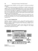
The architecture of the co-simulation environment is kept simple to be as
efficient and accurate as possible. There are two phases to the execution of
the environment: a system generation phase and a runtime support environ-
ment. Each is a standalone process, but both are required for system simula-
tion. Figure 20.26 illustrates this top-level structure.
20.3.1.1 System Generator
The System Generator allows the user to create the necessary files needed
by both Chatoyant and ModelSim. For Chatoyant this includes a common
header and object file used in both simulators as well as components (stars)
used for the Chatoyant side of the interface. The same header and object file
are used for ModelSim
,
in addition to a shared object library file that is used
for invoking the ModelSim FLI when ModelSim is loaded and elaborates a
design.
The main input to this generator is the top-level or interface-specific
VHDL file. This file contains the list of ports that represent the main conduit
Nicolescu/Model-Based Design for Embedded Systems 67842_C020 Finals Page 681 2009-10-2
CAD Tools for Multi-Domain Systems on Chips 681
Top - level
VHDL file
Wrapper
VHDL
FLI share
object file
System generator
Chatoyant
Co-simulation runtime
system
ModelSim
Definitions
library
Chatoyant
star
FIGURE 20.26
Co-simulation top-level structure.
between the digital domain running within ModelSim and the other domains
handled in Chatoyant. When this file is loaded by the System Generator,
the entity portion of the VHDL is parsed and a linked list of the ports is
created. Each node in this linked list contains the port’s name, its direction
(in/out/bidirectional), and its width (1 bit for a signal and n bits for a bus).
Using a graphical user interface, the user can select which ports to include
and the mapping for the analog voltage levels to be converted into and out of
the MVL9 (Multi-Value Logic 9 signal representation standard) logic repre-
sentation used by ModelSim. There are four fields for this including a high,
a low, a cutoff for high, and a cutoff for low voltage values. The user also
specifies a name for the system, used for code generation and library man-
agement. The outputs of the generator phase are the component star file for
Chatoyant, the FLI source code for the ModelSim FLI, the header and source
files for a common resource library for the system, a makefile for remaking
the object files, a usage text file, and the first time compilation object files
performed at the end of the generation.
With these files in place, the user can then proceed with the execution of
the linked simulators.
20.3.1.2 Runtime Environment: Application of Parallel Discrete
Event Simulation
The runtime system differentiates itself from other typical co-simulation
environments in that there is no central simulation management system.
Chatoyant and ModelSim are treated as two standalone processes and
Nicolescu/Model-Based Design for Embedded Systems 67842_C020 Finals Page 682 2009-10-2
682 Model-Based Design for Embedded Systems
communicate only between themselves. This reduces the overhead of
another application executing along with the two simulators as well as the
additional message traffic produced by such an arbiter.
This philosophy is an application of a general parallel discrete event sim-
ulation (PDES) system. Since there are two standalone processes, each is
treated as if it were its own DE processing node. Without a central arbiter,
the two must (1) exchange event information by converting logic values into
voltages and vice versa, and (2) synchronize their respective local simula-
tion times. To exchange the event information, the system uses technology-
specific lookup tables, created by the System Generator, that provide the
conversion between a logic “1” and a logic “0” to a voltage in addition to
determining what voltage level constitutes a logic “1” and “0.”
The synchronization of the simulators is where the application of PDES
methods enters [49]. The asynchronous DE simulation invokes both simula-
tors to perform unique tasks on separate parts of a design in a nonsequential
fashion. This is because of the fact that there is no master synchronization
process as in [1]. For synchronization and scheduling there are two major
approaches one can take, conservative or optimistic. We discuss our choice
next.
20.3.1.3 Conservative versus Optimistic Synchronization
The conservative and optimistic approaches solve the parallel synchroniza-
tion problem in two distinct ways. This problem is defined in [2] as the
requirement for multiple processing elements to produce events of an equal
timestamp in order to not violate the physical causality of the system. The
conservative method solves this problem by constraining each processing
node to remain in synchronicity with the others, never allowing one simula-
tor’s time to pass any other simulator. This can have the penalty of reducing
the performance of a simulation by requiring extra overhead in the form of
communication and deadlock avoidance.
The optimistic approach breaks the rule of maintaining strict causality
by allowing each processing element to simulate without considering time
in other processing element. This means that the simulators can run freely
without having to synchronize, with the exception of communicating explicit
event information. If, however, there is an event sent from one simulator to
the other, and the second simulator has a local current time greater than the
event’s timestamp, then the receiving simulation process must stop and roll-
back time to a known safe state that is before the timestamp of the incoming
event. This approach requires state saving as well as rollback mechanisms.
This can be costly in terms of memory usage and processing overhead for
determining and recalling previous states, and thus increases the processing
time of every event.
Both approaches are possible since ModelSim does have check-pointing
and restoring methods available [48]. However, the conservative PDES
Nicolescu/Model-Based Design for Embedded Systems 67842_C020 Finals Page 683 2009-10-2
CAD Tools for Multi-Domain Systems on Chips 683
method was chosen as the underlying philosophy for our co-simulation
solution. Two factors went into this decision. The first consideration is
that the co-simulation environment is executing as two processes on one
workstation, so that exchanging timing information is not as costly as in a
large physically distributed simulation environment. The second is that even
with a dual-processor workstation, there is not an excess of computational or
memory resources that is seen in a truly distributed PDES architecture, and
therefore, a rollback would be too costly.
This was confirmed with a preliminary test of the fiber image guide sys-
tem described below. For that system the amount of data required for a
checkpoint file was on the order of 1 to 2MB. With an average of 10 check-
point files needed to keep the two simulators within a common time horizon,
rollback time took between 500 ms and 1.5 s.
On the other hand, the conservative approach gives a solution requir-
ing significantly less memory at the expense of increased communication to
ensure that both simulators are consistently synchronized. This becomes a
matter of passing simple event time information between the two simulators.
Thus, the only real design issue becomes the time synchronization method.
20.3.1.4 Conservative Synchronization Using UNIX IPC Mechanisms
As described in more detail below, the system was developed and tested on a
Linux-based workstation. Therefore, UNIX-style IPC is used for the commu-
nication architecture. Event information is exchanged using shared memory,
and synchronization is achieved by using named pipes in blocking mode.
This is similar to the synchronized data transfer and blocking methodology
described in [50]. With these two mechanisms, the conservative approach is
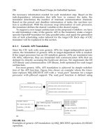
implemented in the two algorithms seen in Figure 20.27.
The algorithm for the co-simulation is straightforward. Both simulators,
running concurrently, reach a point in their respective execution paths where
they enter the interface code in Figure 20.27. Both check to ensure that they
are at the next synchronization point (next_sync), and if they are not, they
exit this section of code and continue. If they are at the next synchroniza-
tion point, defining the safe-point in terms of the conservative approach in
PDES, then Chatoyant starts the exchange by checking for any change in its
outputs to ModelSim. If there is any change in any bit of these ports, that
port is marked dirty, and a change flag is set. When all the ports have been
examined, Chatoyant sends ModelSim either a ModelSim_Bound event, if
any port changed value, or a No_Change event.
Simultaneously, ModelSim waits for this event message from Chatoyant.
Once received, it will update and schedule an event for those ports with dirty
flags set, if any. It then jumps to check its own output ports, checking bit by
bit for a change in each port’s value. Once again, as in Chatoyant, if there is a
difference, the dirty flag for that port is set, and the change flag in ModelSim
is set true. Once this is done for every port, ModelSim will send a message to
Chatoyant that there is either a change (Chatoyant_Bound) or No_Change.
Nicolescu/Model-Based Design for Embedded Systems 67842_C020 Finals Page 684 2009-10-2
684 Model-Based Design for Embedded Systems
Chatoyant ModelSim
If(time < next_sync)
If(time < next_sync)
If(Response = = No_Change)
<check outputs>;
Else
For each input:
For each output:
For each bit in signal:
If(cur[i] ! = new[i])
mark dirty;
flag change;
End If;
End For each bit;
End For each output;
If(change){
send(Chatoyant_Bound);
Else
send(No_Change);
end If;
Synchronize:
next_sync = now + SYNC_PULSE;
Wait(Chatoyant Finished);
Send(ModelSim_Finished);
Done with iteration;
If(input.dirty)
update local value;
ScheduleEvent();
clear input.dirty;
End If;
End For each input;
End If;
return at a later time;
return at a later time;
Wait(Chatoyant_Response);
If(change){
send(ModelSim_Bound);
Else
send(No_Change);
end If;
Wait(ModelSim_Response); // Blocking
If(Response == No_Change)
goto Synchronize;
Else
For each input:
If(input.dirty)
update local value;
ScheduleEventToPorthole();
clear input.dirty;
End If;
End If;
End for each input;
Synchronize:
next_sync = now + SYNC_PULSE;
Send(Chatoyant_Finished);
Wait(ModelSim_Finished);
Done with iteration;
mark dirty;
flag change;
For each output:
For each bit in signal:
If(cur[i] ! = new[i])
End If;
End For each bit;
End For each output;
FIGURE 20.27
The synchronization in both simulators.
Chatoyant, waiting for this response, will receive it and take action sim-
ilar to that of ModelSim in updating the inputs from ModelSim. Finally, the
two will set their respective next synchronization times and handshake with
one another to indicate it is safe to continue simulating. The No_Change mes-
sages are analogous to the null message passing scheme defined by Chandy
and Misra [49], which has the benefit of avoiding simulation deadlock.
A key point is the concept of the next synchronization time (next_sync).
This value is calculated based on a global parameter in the co-simulation
Nicolescu/Model-Based Design for Embedded Systems 67842_C020 Finals Page 685 2009-10-2
CAD Tools for Multi-Domain Systems on Chips 685
environment known as the SYNC_PULSE. This parameter defines the
resolution of how often synchronization occurs. This valueultimately defines
the speed versus accuracy tradeoff ratio between the simulators. A higher
resolution (smaller SYNC_PULSE value) means greater accuracy but slower
runtime. Depending on a particular system, this could affect the quality of
the simulation results.
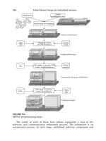
20.3.2 Co-Simulation of Experimental Systems
To examine the effects of synchronization resolution on speed and accuracy,
we simulate two example MDSoC systems. Both are large-scale systems,
meaning there are many components in each domain, including multi-
ple analog circuits, complex optics, and mixed wire and bus interconnects
between the digital and analog domains.
20.3.2.1 Fiber Image Guide
The first of these systems is the fiber image guide, or FIG, system developed
at the University of Pittsburgh [51]. FIG is a high-speed 64 × 64-bit opto-
electronic crossbar switch built using an optical multi-chip module. FIG uses
guided wave optics, analog amplification and filtering circuits, and digital
control logic to create an 8 × 8, 8-bit bus crossbar switch. The switch is built
as a multistage interconnection network (MIN) built with a shuffle-exchange
architecture. The shuffle operations are performed by the wave guide, and
the digital logic performs the exchange switching operation. Analog circuits
amplify the digital signals and drive VCSEL arrays which in turn transmit
light through the image guide. Photodetectors are used to convert the light
back into an analog signal, which is amplified and fed back into the digital
domain.
This system, illustrated in Figure 20.28, exercises the ability of the
co-simulation environment to handle buses as well as the communications
between domains without a synchronous clock. In other words, there is no
clock signal traveling across the co-simulation interface, and thus the events
occur in asynchronous fashion.
20.3.2.2 Smart Optical Pixel Transceiver
The smart optical pixel transceiver, or SPOT, was a development at the Uni-
versity of Delaware [52]. It provides a short-range free-space optical link
between two custom-designed transceivers. Each transceiver either accepts
or generates a parallel bus, in the digital domain. On the transmitter side,
each bus is serialized into a double data rate data signal, along with a 4X
clock (125 MHz clock doubled to 250 MHz in this test system). Serializa-
tion and de-serialization are handled in the digital domain. These serial
data/clock streams are converted into analog signals that are amplified
and used to drive VCSEL arrays, similar to FIG. Photodetectors convert the