Model-Based Design for Embedded Systems- P65 pot
Bạn đang xem bản rút gọn của tài liệu. Xem và tải ngay bản đầy đủ của tài liệu tại đây (565.6 KB, 10 trang )
Nicolescu/Model-Based Design for Embedded Systems 67842_C019 Finals Page 626 2009-10-14
626 Model-Based Design for Embedded Systems
TABLE 19.4
Optical Device Parameters
Source Parameter Min. Value Max. Value Units
Total efficiency 0.1 0.3 mW/mA
Area 10 ×10 100 ×100 μm
2
Threshold current 1.5e-5 1.5e-3 A
Bandwidth 10 GHz
Detector
Responsivity 0.5 0.7 mA/mW
Area 10 ×10 100 ×100 μm
2
Capacitance 1e-15 1e-13 F
Dark current 1e-18 A
Noise current 1e-15 A
Bandwidth 20 GHz
Waveguide SOI Si
3
N
4
Guide index 3.45 2.0
Cladding index 1.46 1.46
Height 0.22 0.8 μm
Width 0.5 0.4 μm
Pitch 1.1e-6 4e-6 m
Loss 2.7 1.5 dB/cm
Delay 13.3 6.7 ps/mm
Excess bend loss 0.027 1.52 dB/90˚
Bend radius 2 10 μm
transmitter and receiver circuits modulate laser current and transform
detector current respectively, through a via stack as represented by R
via
in
Figure 19.8b. Light emitted by an InP laser is transported through a passive
Si/SiO
2
structure at wavelengths around 1.5 μm to an InP or SiGe detector.In
this design approach, no architectural variants are considered (i.e., the CMOS
topologies used at the transistor level are fixed in terms of their structure—
the variables for the design problem consist essentially of bias currents and
transistor sizes).
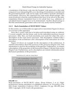
The synthesis approach implemented consists of creating “scenarios”
allowing the specification of each model via a generic class containing all
structures to be optimized, as well as necessary evaluation and design meth-
ods (Figure 19.9). Communication between the different blocks is ensured
using the synthesizable AMS/MT IP blocks, and the actual synthesis and
evaluation scenario relies upon the instantiation of the generic top-level
object in a testbench structure. A device library containing the synthesizable
models of each device in the optical link based on the UML language was
developed to allow the modeling of this hierarchical synthesis problem, as
was already shown in Figure 19.7.
The procedure used to automatically synthesize an optical point-to-point
link, and implemented as a synthesis scenario, is shown in Figure 19.10. The
Nicolescu/Model-Based Design for Embedded Systems 67842_C019 Finals Page 627 2009-10-14
Platform for Model-Based Design of Integrated Multi-Technology Systems 627
CMOS transistor layer
(a)
(b)
Absorption
layer
n-Contact
p-Contact
III–V input
waveguide
III–V photodetector
Si photonic waveguide (n= 3.5)
SiO
2
waveguide cladding (n= 1.5)
III–V laser source
Active layer
Via
stack
n-Contact
p-Contact
Copper interconnect layers
Comparator
v
out
v
i
V
ref
V
dd
V
d
V
p
i
photo
i
source
i
m
I
B
M
m
M
r
Buffers
Current
modulation
Transimpedance
amplifier
M
b
V
bias
M
3
M
2
M
1
R
f
R
via
R
via
–
+
FIGURE 19.8
Integrated optical link (a) physical implementation (b) schematic.
process starts by defining the photodetector characteristics and the required
data rate. Using a transistor-level synthesis method described in [OCO2003],
the transistor-level schematic for the transimpedance amplifier is automati-
cally generated and linked to a manually scaled comparator circuit.
The value of the rms noise power, i
n
, is extracted from the simulation
of the schematic, and updated for each synthesis loop, using the Morikuni
formula [MOR1994] in the transimpedance amplifier noise calculations:
i
2
N
=
2q
I
gate
+I
dark
+
4kT
R
f
C
4D
+4kTΓ
C
2
16π
2
DE
(
2πC
r
)
2
g
m
Nicolescu/Model-Based Design for Embedded Systems 67842_C019 Finals Page 628 2009-10-14
628 Model-Based Design for Embedded Systems
Synthesizable
(from interfaces)
Evaluatable
(from interfaces)
Test
S1
#link: OPP link
#vs: Vsource
<<realize>>
Genericlink
#BER: double
#Power: double
#Area: double
#Data rate: double
#Vin: electrical node
#Vout: electrical node
+main( ): void
<<create>>+S1(): S1
OPP link
-driver: Driver
-source: Source
-waveguide structure: Waveguide structure
-detector: Detector
-receiver: Receiver
+evaluate(): void
<<create>>+opplink(): OPP link
Optical point to point
link defines
structure
Generic link defines
performance criteria
Evaluation scenario defines:
- setup procedure
- evaluation method invocation
Test defines general
structure necessary for
evaluation
Synthesis scenario defines
- setup procedure (top-level specifications)
- structural choices, selection algorithm
- parameter choices, optimization algorithm(s)
FIGURE 19.9
Definition of classes in UML for test benches, evaluation and synthesis scenarios for the integrated optical link.
Nicolescu/Model-Based Design for Embedded Systems 67842_C019 Finals Page 629 2009-10-14
Platform for Model-Based Design of Integrated Multi-Technology Systems 629
Data rate D
V
did
Transistor
models
Transimpedance
amplifier circuit
Amplifier circuit
Analog synthesis
i
n
= i
nTIA
+i
dark
ΔP
t
=ΔP
r
/10
–loss/10
Input referred
TIA noise
current i
nTIA
Photodetector
dark current i
dark
SNR
Δ
P
t
Δ P
r
i
n
I
mod
I
bios
I
mod
= ΔP
t
/η
s
I
bias
= 1.1 I
t
Loss = L × k
Loss
SNR = 8[erfc
–1
(2BER)]
2
Photonic
technology
System
specifications
CMOS
technology
Waveguide loss/cm k
Link length L
ΔP
r
=i
n
× SNR
Source threshold current l
t
Source efficiency η
s
Current
modulation and
bias circuits,
buffer circuits
A
v,
R
o
C
m
C
in
C
out
Photodetector capacitance C
d
Output dynamic ΔV
out
Bit error
rate BER
FIGURE 19.10
Optical link sizing method.
where
C = 1 + g
m
R
f
D = R
o
C
x
+C
y
+R
f
(
C
x
+C
m
)
+g
m
R
f
R
o
C
m
E = R
f
R
o
C
x
+C
y
C
m
+C
x
C
y
For a given bit error rate (BER) specification and noise signal associated with
the photodiode and transimpedance circuit, we can then calculate the min-
imum optical signal power, ΔP
s
, required by the receiver to operate at the
given error probability:
ΔP
s
= i
n
×SNR
where
SNR =
erfc
−1
(
2 BER
)
Here, SNR represents the linear signal to noise ratio (absolute value, not in
dB). BER, defined as the rate of error occurrences, is oneofthe main criteria in
evaluating the performance of digital transmission systems. In our analyses
we fixed BER at 10
−18
bits
−1
(this corresponds to 1 error / 3.17 years for a
single link at 10 Gbps communication, or 1 error/18 days for a 64-bit data
bus at the same data rate.)
The value of the power that needs to be emitted by the laser source is
evaluated from the calculated value of the minimum optical power at the
Nicolescu/Model-Based Design for Embedded Systems 67842_C019 Finals Page 630 2009-10-14
630 Model-Based Design for Embedded Systems
receiver, and from the power losses induced by the geometry of the waveg-
uide structure (length and intrinsic loss, number of bends, and loss/90˚bend)
and coupling. These figures depend to a large extent on the materials used
and are defined in Table 19.4.
The final sizing step is to calculate the driver and associated bias and
buffer circuits using the emitted power value and the source characteristics
in conjunction with the method shown in Figure 19.10. This then enables
the simulation of the complete optical link, using transistor-level schematics
for the interface circuits and the developed behavioral models for the pho-
tonic devices. From the simulation results, the performance criteria can be
extracted.
Using this approach, the synthesis problem is considered to be complete,
such that no constraint partitioning is required. In fact, the constraints are
derived directly from system specifications, and thus constraint exploration
is achieved directly by the user.
19.3.3 Performance Metrics and Specification Sets
In order to be able to evaluate and optimize link performance criteria cor-
rectly, a clear definition of the performance metrics is required. First, the aim
is to establish the overall power dissipation for an optical link at a given
data rate and BER. The calculation is essentially conditioned by the receiver
as explained above, since the BER defines the lower limit for the received
optical power. This lower limit can then be used to calculate the required
power coupled into waveguides by optical sources, the required detector
efficiency (including optical coupling), and acceptable transmission losses.
Power can then be estimated from source bias current and photoreceiver
front-end design methodologies.
For interconnect density aspects, source and detector sizes must be taken
into account, while the width, pitch, and required bend radius of waveguides
is fundamental to estimating the size of the photonic layer. On the circuit
layer, the additional surface due to optical interconnect is in the driver and
receiver circuits, as well as the depassivated link to the photonic layer. The
circuit layout problem is compounded by the necessity of using clean supply
lines (i.e., separate from digital supplies) to reduce noise (for BER).
The data rate is essentially governed by the bandwidth of the photore-
ceiver: high modulation speed at the source is generally more easily attain-
able than similar detection speed at the receiver. This is largely due to
the photodiode parasitic capacitance at the input of the transimpedance
amplifier.
The limitations of this analysis as carried out here are that
• Predictive technology model (PTM)
∗
models do not take noise into
account particularly well, which means that no real noise analysis can
∗
Predictive Technology Model ( />Nicolescu/Model-Based Design for Embedded Systems 67842_C019 Finals Page 631 2009-10-14
Platform for Model-Based Design of Integrated Multi-Technology Systems 631
be carried out. However in the sizing process this problem was circum-
vented by using the Morikuni formula to estimate noise at block level,
as previously described.
• No automatic layout generation tools were used, as it is not in gen-
eral possible to achieve optimal layout for high-speed analog circuits.
Parasitic capacitances were therefore extracted from layout estimations
using lambda rules [OCO2007] rather than from actual layouts.
19.4 Integrated Optical Interconnect Investigation
Program and Results
In this section, we cover the values of the performance metrics generated
by the synthesis procedures described in the previous section. The analyses
were carried out for
• Two sets of optical device parameters as described in Table 19.4, which
will be denoted in the following analyses as S1 (“pessimistic” values)
and S2 (“optimistic” values)
• Three predictive technologies (gate lengths of 65, 45, and 32 nm) using
PTM models and frequencies defined by the ITRS (as local clock fre-
quencies) for the corresponding technology nodes
• Various optical link lengths from 2.5 mm to the maximum chip side
dimension (20 mm)
Table 19.5 shows the sets of specifications used for analysis and interface
circuit sizing and to demonstrate the capacity of the platform and imple-
mented method to synthesize optical links subject to technological specifi-
cations, both CMOS and optical. The generation of each data point requires
approximately 5 min on a 1.3 GHz processor with 4 Gb memory.
TABLE 19.5
Link Specification Set
Scenario
Parameter PTM65 PTM45 PTM32
BER bit
−1
10
−18
10
−18
10
−18
ITRS max. frequency bit/s 2.98 × 10
9
5.20 ×10
9
1.10 ×10
10
Link length mm {2.5,20} {2.5,20} {2.5,20}
Activity rate 1 1 1
Ambient temperature ˚C 70 70 70
V
dd
(CMOS) V 1.2 1.1 1.0
Nicolescu/Model-Based Design for Embedded Systems 67842_C019 Finals Page 632 2009-10-14
632 Model-Based Design for Embedded Systems
The results obtained were compared to the performance of 1.1 μmpitch
unshielded electrical interconnect, synthesized with another toolset and
using the same specifications as drivers for the synthesis process [OCO2007].
The simulation conditions were
• Inverters (as buffers for each electrical interconnect segment) with a
2/1 PMOS-to-NMOS ratio were used.
• For each CMOS technology used, the maximal overall link input capac-
itance was restricted to that of a CMOS inverter with minimal gate
length (defined as 2 λ) and 60λ and 30λ for the PMOS and NMOS
widths, respectively.
• The minimal output drive strength was set to that of the same inverter.
The comparison results are presented in the form of reduction factors, cal-
culated as P
e
/P
o
, where P
o
represents the optical performance figure and
P
e
represents the electrical interconnect figure (where smaller performance
figures for area, delay, and power mean improved performance).
19.4.1 Gate Area Analysis
The link sizing method described in Section 19.3.2 was applied according to
the specifications for the PTM 65, 45, and 32 nm technologies. Figure 19.11
shows the results in terms of gate area (i.e., transistor channel dimensions
only), extracted as the sum of all transistor gate channel areas W ·L. These
results show that the gate area metric approximately verifies the scaling law
(A
32nm
≈ A
45nm
·s
2
≈ A
32nm
·s
2
·s
2
), where s is equal to 0.7 (scaling factor
between technology generations).
The specification set S
2
reduces total CMOS gate area by a factor of
between 2 (BPT 32 nm) to 4 (BPT 65 nm) with respect to S
1
. These figures
demonstrate an impressive reduction in gate area in favor of optical intercon-
nect (of the order of 60x–90x for link lengths above 1 cm and for the two most
advanced technology nodes) with respect to electrical interconnect. Optical
interconnect will thus introduce a significantly lower area penalty for data
routing functions at transistor level. These figures are to be considered in the
context of scenarios indicating the use of up to 25% of transistors on chip
in electrical interconnect buffers. While only a part of this number is used
for long links, it is still clear that the use of optical links will free up a large
number of transistors for use in functions other than interconnect (data pro-
cessing, memory, etc.).
19.4.2 Delay Analysis
The link sizing method described in Section 19.3.2 was applied according
to the specifications for the PTM 65, 45, and 32 nm technologies. The 50%
Nicolescu/Model-Based Design for Embedded Systems 67842_C019 Finals Page 633 2009-10-14
Platform for Model-Based Design of Integrated Multi-Technology Systems 633
6
5
4
3
2
1
0
2.5 7.5 10 12.5 15 2017.55
Total CMOS gate area (μm
2
) vs. interconnect length—optical link
BPT 32 S
1
– 1.1μm pitch
BPT 45 S
1
– 1.1μm pitch
BPT 65 S
1
– 1.1μm pitch
BPT 65 S
2
– 1.1μm pitch
BPT 32 S
2
– 1.1μm pitch
BPT 45 S
2
– 1.1μm pitch
Link length (mm)(a)
(b)
BPT 65 S
1
– 1.1μm pitch
BPT 65 S
2
– 1.1μm pitch
BPT 45 S
1
– 1.1μm pitch
BPT 45 S
2
– 1.1μm pitch
BPT 32 S
1
– 1.1μm pitch
BPT 32 S
2
– 1.1μm pitch
100
90
80
70
60
50
40
30
20
10
0
0 5 10 15 20 25
Link length (mm)
Gate area reduction factor vs. interconnect—length
FIGURE 19.11
(a) Total CMOS gate area (μm
2
) for varying optical interconnect length and
technologies (b) Gate area comparison for varying interconnect length and
technologies at 1.1 μm pitch : reduction factor.
propagation delay was extracted from simulation as
Δt = t
V
out
=
V
pit
max
+V
out
min
2
,slope=+,5
−t
V
in
=
V
in
max
+V
in
min
2
,slope=+,5
where the notation
t
V=V
1
,slope=
{
+,−
}
,n
Nicolescu/Model-Based Design for Embedded Systems 67842_C019 Finals Page 634 2009-10-14
634 Model-Based Design for Embedded Systems
signifies the time corresponding to the nth simulation point where the
quantity V is equal to V
1
on a rising (+) or falling (–) slope. Also calculated
as a point of reference was the intrinsic waveguide delay, using τ
TOF
= 13.3
ps/mm for the Si/SiO
2
waveguides.
∗
Figure 19.12 shows the delay results
for varying link lengths.
It can be seen that (a) the circuit delay (i.e., the difference between the total
delay and the intrinsic waveguide delay) decreases with smaller gate lengths,
and (b) the same quantity also decreases with longer interconnect. This latter
effect is because of higher driver modulation current, I
m
, required to compen-
sate higher overall waveguide loss, being able to drive the source capacitance
faster and thus tends toward a small contribution to overall delay. As such
the delay is dominated at these lengths by detector and source delay, waveg-
uide delay, and comparator delay. Since these parameters do not change
between S
1
and S
2
, no significant improvement can be observed between
the results for these two optical parameter sets. At best, a further 50 ps delay
reduction can be achieved at the shorter link lengths (where optical links are
less likely to be used).
With respect to electrical interconnect, it is shown that optical intercon-
nect will have a slight advantage in terms of delay for long interconnect
lengths (above 10 mm). The underlying reason for this is that delay for optical
interconnect does not depend as strongly on interconnect length as electrical
interconnect, because no additional circuit stages are added—the increase
stems from higher intrinsic waveguide delay only. However, the advantage
decreases for more advanced technology nodes and indeed does not achieve
any delay reduction (actually the opposite) for unscaled interconnect at 32
nm gate length.
19.4.3 Power Analysis
The link sizing method described in Section 19.3.2 was applied according to
the specifications for the PTM 65, 45, and 32 nm technologies. The average
static power was extracted from transient simulations using
¯
P =
I
source
0
+I
source
1
2
·V
p
+
I
det
0
+I
det
1
2
·V
d
I
cct
0
+I
cct
1
2
·V
dd
where I
source
, I
det
,andI
cct
represent the currents flowing through the source,
detector, and circuit voltage supplies of V
p
, V
d
,andV
dd
, respectively. Fig-
ure 19.13a shows the average static power results for varying link lengths.
Figure 19.13b shows the dynamic power results for varying link lengths,
calculated from rising and falling edge transitions (the average switching
energy extracted from simulations as the integral of supply currents in edge
transitions).
Significant reductions in static power are observed between S
1
and S
2
(a
minimum factor of 2 for BPT 45 and 3 for BPT 32 at low link lengths; and a
∗
TOF, time of flight.
Nicolescu/Model-Based Design for Embedded Systems 67842_C019 Finals Page 635 2009-10-14
Platform for Model-Based Design of Integrated Multi-Technology Systems 635
Total link delay (ps) vs. interconnect length—optical link
Link length (mm)(a)
(b)
BPT 32 S
1
–1.1μm pitch
Intrinsic waveguide delay (SiO
2
)
BPT 45 S
1
–1.1μm pitch
BPT 65 S
1
–1.1μm pitch
BPT 32 S
2
–1.1μm pitch
BPT 45 S
2
–1.1μm pitch
BPT 65 S
2
–1.1μm pitch
450
400
350
300
250
200
150
100
50
0
2.5 5 7.5 10 12.5 15 17.5 20
Delay reduction factor vs. interconnect length
Link length (mm)
3.0
2.5
2.0
1.5
1.0
0.5
0.0
0 5 10 15 20 25
BPT 65 S
1
–1.1μm pitch
BPT 45 S
1
–1.1μm pitch
BPT 32 S
1
–1.1μm pitch
BPT 65 S
2
–1.1μm pitch
BPT 45 S
2
–1.1μm pitch
BPT 32 S
2
–1.1μm pitch
FIGURE 19.12
(a) Total link delay (ps) for varying optical interconnect length and technolo-
gies. (b) Delay comparison for varying interconnect length and technologies
at 1.1 μm pitch : reduction factor.
maximum factor of 4 for BPT 65 and BPT 32 at high link lengths). This result
is due mainly to the lower source threshold current, but also to higher source
efficiency and detector responsivity leading to lower modulation currents,