Model-Based Design for Embedded Systems- P64 pot
Bạn đang xem bản rút gọn của tài liệu. Xem và tải ngay bản đầy đủ của tài liệu tại đây (551.71 KB, 10 trang )
Nicolescu/Model-Based Design for Embedded Systems 67842_C019 Finals Page 616 2009-10-14
616 Model-Based Design for Embedded Systems
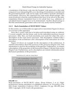
Lower structural hierarchical level n–1
Distribution
Model parameter
values
Search engine
Search
Update
Firm IP
library
(XML)
Update
Performance values
Aggregation
Design variables to
physical parameter
conversion method
*r
Components of
soft-IP library
Specification values
Error function
calculation
1-Step optimization
Design variables,
physical parameters
Constraint distribution
method
Parameter extraction
method
Evaluation
method
Extraction
(aggregation)
Raw results
Simulation/execution
Behavioral
model
Stimuli
Loads
Structural modal
(Jig/code)
Measures
Synthesis
method
Performance
criteria
Design variables
V
Constraint distribution
method
*c
Synthesis method
*m
Evaluation and parameter
extraction methods
*e
Physical parameters
P
Performance criteria
S
Higher structural hierarchical level n+1
FIGURE 19.4
Single-level AMS/MT synthesis loop showing context of AMS/MT IP facet use.
Nicolescu/Model-Based Design for Embedded Systems 67842_C019 Finals Page 617 2009-10-14
Platform for Model-Based Design of Integrated Multi-Technology Systems 617
(w
i
∀i ∈ {0,n − 1}) and normalized squared differences subject to speci-
fication type (constraint, cost, condition, etc.):
ε =
i=n−1
i=0
w
i
s
i
−s
ri
s
i
2
This comparison between specified and real performance criteria values,
the error function in Figure 19.4, drives
∗
m, the synthesis method, which
describes the route to determine design variable values. It is possible to
achieve this in two main ways:
• Through a direct procedure definition, if the design problem has suffi-
cient constraints to enable the definition of an explicit solution.
• Through an iterative optimization algorithm. If the optimization pro-
cess cannot, as is usually the case, be described directly in the language
used to describe the IP block, then a communication model must be set
up between the optimizer and the evaluation method. A direct com-
munication model gives complete control to the optimization process,
while an inverse communication model uses an external process to
control data flow and synchronization between optimization and eval-
uation. The latter model is less efficient but makes it easier to retain
tight control over the synthesis process [MAS1991].
The synthesis method generates a new set V of combinations of design
variables as exploratory points in the design space according to *m:S→V.
The number of design variables defines the number of dimensions of the
design space. The design variables must be independent of each other, and
as such represent a subset of IP block parameters (i.e., performance crite-
ria, described above) in a structure definition. For example, a differential
amplifier design variable subset could be reduced to a single gate length, bias
voltage, and three transistor widths for the current source, matched ampli-
fier transistors, and matched current mirror transistors. Physical variables
(in the set P, which outputs to the model parameter values in Figure 19.4)
are directly related to design variables according to a mapping method
∗
r
such that *r:V→P, and serve to parameterize all components in the structure
definition during the IP block evaluation process. In the above example, the
design variable subset would be expanded to explicitly define all component
parameters.
The evaluation method ∗e, at the left of Figure 19.4, describes the route
from the physical variable values to the performance criteria values such
that *e:P→S, and thus completes the iterative single-level optimization loop.
Evaluation can be achieved in two main ways:
• Through direct code evaluation, such as for active surface area
calculations.
• Through simulation (including behavioral simulation) for accurate
performance evaluation (gain, bandwidth, distortion, etc.). If the IP
Nicolescu/Model-Based Design for Embedded Systems 67842_C019 Finals Page 618 2009-10-14
618 Model-Based Design for Embedded Systems
block is not described in a modeling language that can be understood
by a simulator, then this requires a gateway to a specific simulator
and to a jig (a set of files to describe the environment surrounding the
IP block and the stimuli to be applied in order to extract meaningful
indicators of performance) corresponding to the IP block itself. For the
simulator, this requires definition of how the simulation process will
be controlled (part of the aforementioned communication model). For
the jig, this requires the transmission of physical variables as param-
eters, and the extraction of performance criteria from the simulator-
specific results file. The latter describes the role of the parameter
extraction method, which is necessary to define how the design pro-
cess moves up the hierarchical levels during bottom-up verification
phases.
Once the single-level loop has converged, the constraint distribution method
∗
c defines how the design process moves down the hierarchical levels dur-
ing top-down design phases, and defines the specifications for the lower
hierarchical structural level n – 1 in Figure 19.4. At the end of the synthe-
sis process at a given hierarchical level, an IP block will be defined by a
set of physical variable values, some of which are parameters of an IP sub-
block. To continue the design process, the IP subblock will become an IP
block to be designed and it is necessary to transform the block parameters
into specifications according to ∗c : P
k
→S
k+1
(where k represents the struc-
tural hierarchy level). This requires a definition of how each specification
will contribute to the error function ε for the synthesis method in the new
block.
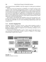
19.2.2 UML/XML Implementation
We have incorporated these concepts into an existing in-house AMS/MT
synthesis framework, Rune
II
. A schematic showing the various inputs and
data files is given in Figure 19.5. From the user’s point of view, there are
two main phases to AMS/MT synthesis: AMS/MT soft-IP definition, which
can be done via UML, XML, or through a specific GUI (all inputs are
interoperable—the internal database format is XML); and AMS/MT firm-IP
synthesis, which can be run from the GUI or from scenarios.
At the system level, in order to enable the satisfactory partitioning of
system-level performance constraints among the various digital, software,
and AMS/MT blocks in the system architecture, top-down synthesis func-
tionality needs to be added to AMS/MT blocks. The goal of this approach
is to enable accurate prediction of analog/RF architectural specification val-
ues for block-level synthesis in an optimal top-down approach by making
reasoned architectural choices about the structure to be designed. For gen-
eral compatibility with system-level design flows, we chose to represent this
aspect with UML. UML 2.0, adopted as a standard by Object Management
Nicolescu/Model-Based Design for Embedded Systems 67842_C019 Finals Page 619 2009-10-14
Platform for Model-Based Design of Integrated Multi-Technology Systems 619
AMS firm IP synthesis
AMS soft IP definition
User
UML XML XMLGUI
Firm IP
.class
Soft IP
.java
FIGURE 19.5
UML/XML/GUI use flow in Rune
II
.
Group (OMG) in 2005, consists of graphical
∗
languages enabling the expres-
sion of system requirements, architecture, and design, and is mainly used
in industry for software and high-level system modeling. The use of UML
for high-level SoC design in general appears possible and has generated
interest in several research and industrial groups [RIC2005]. For AMS/MT
systems, [CAR2004] demonstrated the feasibility of describing AMS/MT
blocks in UML and then translating them to VHDL-AMS, building on other
approaches to use a generic description to target various design languages
[CHA2004]. Considerable effort is also being put into the development of
“AMS/MT-aware” object-oriented design languages such as SystemC-AMS
[VAC2003] and SysML [VAN2005]. These languages can be linked to a UML
approach (SysML is directly derived from UML, and SystemC as an object-
oriented language can be represented in UML also), and as such it should be
possible to map UML-based work to these derived or related languages.
In order to develop a UML-based approach to hierarchical AMS/MT syn-
thesis, it is necessary to map the AMS/MT IP element requirements given in
Table 19.3 to UML concepts. UML has many types of diagrams, and many
concepts that can be expressed in each—many more, in fact, than are actu-
ally needed for the specific AMS/MT IP problem. Concerning the types of
diagram, two broad categories are available:
∗
A language for textual representation of UML diagrams also exists (OCL—Object Con-
straint Language. />Nicolescu/Model-Based Design for Embedded Systems 67842_C019 Finals Page 620 2009-10-14
620 Model-Based Design for Embedded Systems
• Structural diagram, to express the static relationship between the
building blocks of the system. We used a class diagram to describe
the properties of the AMS/MT IP blocks and the intrinsic relations
between them. The tenets of this approach and how to generate UML-
based synthesizable AMS/MT IP will be described in this section.
• Behavioral diagram, showing the evolution of the system overtime
through response to requests, or through interaction between the sys-
tem components. An activity diagram can be used to describe the
AMS/MT synthesis process [OCO2006].
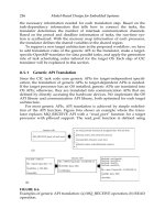
To describe class relationships for AMS/MT IP blocks, it is first necessary
to establish a clear separation of a single function definition (entity and
functional-level model for top-down flows) from n related structural mod-
els (for single-level optimization and bottom-up verification). Each struc-
tural model contains lower-level components, which should be described by
another function definition. It is also necessary to establish functionality and
requirements common to all structural models whatever their function. By
representing all this in a single diagram, shown in Figure 19.6a, we are in
fact modeling a library of system components; not the actual system to be
designed itself.
A class diagram constitutes a static representation of the system. It
allows the definition of classes among several fundamental types, the class
attributes and operations, and the time-invariant relationships between the
various classes. From the above analysis, we require
• A single, noninstantiable (abstract) class representing common func-
tionality and requirements, in a separate publicly accessible package.
We called this class topology.
• A single class representing the function definition, which inherits from
topology. An alternative solution would be to separate “evaluatable”
functionality and “synthesizable” functionality through the use of
interfaces. This is certainly a debatable point, but our view is that it
would tend to overcomplicate the description process. Another point
is that one can also be tempted to separate the entity aspect from the
behavioral model aspect, which would then allow the entity class to
become abstract. Again, this also appears to be somewhat overcompli-
cated to carry out.
• A number of classes representing the structural models, which all
inherit from the function definition class. Each structural variant is
composed of a number of components at a lower hierarchical level, rep-
resented by a single function definition class for each component with
different functionality. As the structural variant cannot exist if the com-
ponent classes do not exist, this composition relationship is strength-
ened to an aggregation relationship.
Having established how to separate particular functionality between com-
mon, functional, and structural parts of an AMS/MT hierarchical model,
Nicolescu/Model-Based Design for Embedded Systems 67842_C019 Finals Page 621 2009-10-14
Platform for Model-Based Design of Integrated Multi-Technology Systems 621
Class A
Topology (from common)
Element0_functional
Element1_functional
(a)
Element2_functional
Element0_structural0
1
1 *
1
1 *
1
1 *
1
1 *
Element0_structural1
Inherits from
Is a component of
Class A
Class B
Class B
(update performance criteria
values)
(b)
#name:String
#instancename:String
Functional description
Structural model
#VarName:Specification
Design and physical
variables
(name, units, default values)
+evaluate():void
(structural architecture
model,
bottom up performance
aggregation)
+optimize():void
(synthesis method)
+abstractToPhysical():void
(physical variable calculation)
+descent():void
(call instance top down
methods)
+setVariables():void
(set up variable vectors)
#Specname:Specification
Generic specifications /
Performance criteria
(name, units, default values)
+evaluate():void
(behavioral architecture
model)
+physicalToSpecifications():
void
(generic specification
distribution)
+selectTopology():void
(choice of most suitable
structure)
+setPerformances():void
(set up performance criteria
vector)
#physical:InstanceVector
#abstracts:InstanceVector
#performances:Extended
Vector
#code:String
(specific synthesis
procedure)
(vector of performance
criteria)
+evaluate():void
(evaluate prototype)
+setOptimizer():void
+optimize():void
(optimization process)
+updateSpecifications():void
(define optimization
algorithm)
(vector of physical variables)
(vector of abstract variables)
(model name)
Topology
FIGURE 19.6
(a) UML class diagram showing representation of hierarchical dependen-
cies between AMS/MT IP blocks. (b) UML class definitions for hierarchically
dependent AMS/MT IP blocks.
Nicolescu/Model-Based Design for Embedded Systems 67842_C019 Finals Page 622 2009-10-14
622 Model-Based Design for Embedded Systems
each facet of the AMS/MT IP requirements set out in Table 19.3 can be
included in the various model types, asshownin Figure 19.6b. It is worth not-
ing that the performance criteria and variables are defined with type “spec-
ification.” This is a specific data type, which plays an important role in the
definition of AMS/MT IP, as will be seen in the following sections on the
example optical interconnect application.
19.3 Multi-Technology Design Exploration Application:
Integrated Optical Interconnect
Rune
II
has been extensively used in the exploration of integrated optical
interconnect tradeoffs, both (1) to automatically size interface circuits accord-
ing to link specifications and technology characteristics, thus enabling com-
plete sizing of the optical link; and (2) to explore the impact of optical or
photonic device characteristics on link performance and thus extract data
leading to the identification of bottlenecks at the device level. Because of the
very diverse nature of the exploration space variables, and the level of detail
required in the investigations and analyses, this work could only be carried
out using an automated and predictive simulation-based synthesis approach.
In this section, we will cover the establishment of models required for the
simulation and synthesis of an integrated optical link; the development and
implementation of the specification- and technology-driven optical point-to-
point link synthesis method; and the definition of the performance metrics
and specification sets to be used in the investigation program.
19.3.1 Models for the Simulation and Synthesis of an Optical Link
In order to extract meaningful physical data from analyses where advanced
CMOS technologies are involved and accurate device models are key to
the relevance of investigation, it is essential to work toward design tech-
nology including the simulation of a complete optical point-to-point link
in an EDA framework. A direct consequence of this is that it is necessary
to develop behavioral models for the optoelectronics devices and passive
waveguides, for concurrent simulation with the transistor-level interface cir-
cuit schematics. For all behavioral models, the choice of an appropriate level
of description is a prerequisite to developing and using the models in the
required context. Essentially, the description level falls into one of two cate-
gories: functional modeling or structural modeling (this is a particular case of
model types mentioned in Section 19.2.3). A functional model will describe
the behavior of a device according to its specifications and behavioral equa-
tions, without defining the structure of the device. A structural model will
describe the behavior of a device according to its internal structure and
Nicolescu/Model-Based Design for Embedded Systems 67842_C019 Finals Page 623 2009-10-14
Platform for Model-Based Design of Integrated Multi-Technology Systems 623
physical parameters, without necessarily satisfying the specification criteria
(which do not have to be formalized in this approach).
Ideally, both functional and structural models should exist for all devices
considered. However, this is not absolutely necessary, and careful consid-
eration was given to choosing the appropriate description level for each
device. Since the source behavior is arguably the most complex and likely to
exhibit nonlinear behavior (thermal roll off, temperature changes) important
to complete link simulation, it was decided to model this element at a struc-
tural level. The nonlinear behavior of the microsource laser was modeled
(enabling the visualization of physical limits) and converges systematically
in Spectre. The waveguide and detector were modeled at a functional level.
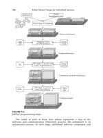
The organization of the interface circuit and active optoelectronic device
model libraries, complying to the UML modeling rules set out in Section
19.2.3, are shown in Figure 19.7a and b respectively.
The models were all implemented in the OVI-96 Verilog-A subset of
Verilog-AMS, an extension of the IEEE 1364-1995 Verilog hardware descrip-
tion language (VHDL). This extension is an industry standard for ana-
log simulation model description and can be simulated with a number of
general-purpose circuit simulators (we used Spectre). This way, the optical
and photonic devices can be simulated together with the interface circuitry
and with the rest of the optical link given adequate simulation models. This
enables interesting optimization strategies (e.g., joint power optimization)
and the analysis of link performance sensitivity to various parameter varia-
tions as well as temperature changes.
Detailed description of these models is outside the scope of this chapter,
but the device parameters for optical interconnect varied in this analysis are
shown in Table 19.4, with minimum and maximum values defining the limits
of the parameter variation. These limits are based on discussions with experts
in the field and on data available in the literature on sources, waveguides,
and detectors [BIN2005,FU2004,FUJ2000,ROE2006,SAK2001,VAN2007]. The
values in bold italics represent the (pessimistic) nominal values.
Achieving complete link simulation was a necessary step to enable sub-
sequent simulation-based link synthesis (using interface circuit design vari-
ables) over a range of target technologies and specification sets to extract link
performance data. The iterative optimization step is facilitated by the low
simulation time required for the complete link (a few seconds for 10 data bits
on a 1.3 GHz processor).
19.3.2 Optical Point-to-Point Link Synthesis
The objective of our work was to carry out transistor-level sizing of the
receiver and of the driver circuits according to complete link specifications.
The optical link under consideration is shown in Figure 19.8. This includes,
as shown in Figure 19.8a, a photonic communication layer integrated above
a standard CMOS circuit above the metallic interconnect layers. CMOS
Nicolescu/Model-Based Design for Embedded Systems 67842_C019 Finals Page 624 2009-10-14
624 Model-Based Design for Embedded Systems
#Quiescent power:double
#Area double
#Modulation speed:double
#Modulation current:double
#Vin:electrical node
#lout:electrical node
Currentmodulation
FunctionalDriver
Inheritance
Type
Performance criteria
Types define
performance
criteria
Realizations define
evaluations (and
synthesis)
Realizations
Contains
Separation between
-type of block
-block realization
(a)
Amplifier
<<create>>+FunctionalDriver():FunctionalDriver
<<create>>+TIAComparator():TIAComparator
+evaluate():void
-Zg():double
<<create>> + FunctionalReceiver():FunctionalReceiver
<<create>> + Receiver():Receiver
<<create>> + Receiver( ):Receiver
#Quiescent power:double
#Area:double
#Speed:double
#Gain
#NoiseRms:double
#lin:Electrical node
#Vout:Electrical node
<<create>> + FunctionalReceiver( ):FunctionalReceiver
+ evaluate():void
-w():double
-Q:double
-QuiescentPower:double
-Area:double
-Ao:double
Synthesizable
(from interfaces)
<<realize>>
<<realize>>
<<realize>>
-Comparator
-tia
<<realize>>
Evaluatable
(from interfaces)
-Ro:double
-QuiescentPower:double
-Area:double
TIA Comparator
Simple
TIA
Receiver
Functional receiver
-Mbias:P mos()
<<create>>+Currentmodulation():Currentmodulation
<<create>>+FunctionalDriver( ):FunctionalDriver
+evaluate():void
+ evaluate():void
<<create>> + Driver():Driver
<<create>> + Driver( ):Driver
#Bias current:double
Driver
FIGURE 19.7
UML class diagram showing representation of hierarchical dependencies between AMS/MT IP blocks (a) CMOS interface
circuit model library (b) active optoelectronics device model library.
Nicolescu/Model-Based Design for Embedded Systems 67842_C019 Finals Page 625 2009-10-14
Platform for Model-Based Design of Integrated Multi-Technology Systems 625
#Threshold current:double
#Capacitance:double{Capacitance>0.0}
#Total efficiency:double{Total efficiecny<=1.0,Total efficiency>=0.0}
#Bandwidth:double{Bandwidth>0.0}
#Area:double{Area>0.0}
#Dark current:double
#Noise:double
#Oin:Electrical node
#lout:Optical node
<<create>>+Detector():Detector
<<create>>+Detector( ):Detector
#Total efficiency:double{Total efficiency<=1.0, total efficiency>=0.0}
#Bandwidth:double{Bandwidth>0.0}
#Area:double{Area>0.0}
#In:Electrical node
#Oout:Optical node
<<create>> + Source():Source
<<create>> + Source( ):Source
<<create>> + Functional source():Functional source
<<create>> + Functional source( ):Functional source
<<create>> + SC_udiskEvanescent():SC_udiskEvanescent
<<create>> + UC_CP evanescent():UC_CP evanescent
+ evaluate():void
(b)
<<create>> + UC_CPDiffractive():UC_CPDiffractive
<<create>> + FunctionalDetector():FunctionalDetector
<<create>> + FunctionalDetector( ):FunctionalDetector
<<create>> + Stack():Stack
<<create>> + Tapered Stack():Tapered Stack
+ evaluate():void
+ evaluate():void
+ evaluate():void
+ evaluate():void
+ evaluate():void
+ evaluate():void
Source
Detector
Functional source
FunctionalDetector
SC_udisk evanescent
UC_CPDiffractive
Structural models describe
behavior based on:
- component block performance
- extracted data (measurement
or simulation)
Functional models describe
behavior based on specs
Synthesizable
(from interfaces)
Evaluatable
(from interfaces)
Stack
TaperedStack
UC_CPEvanescent
FIGURE 19.7 (continued)