Model-Based Design for Embedded Systems- P63 pptx
Bạn đang xem bản rút gọn của tài liệu. Xem và tải ngay bản đầy đủ của tài liệu tại đây (472.65 KB, 10 trang )
Nicolescu/Model-Based Design for Embedded Systems 67842_C019 Finals Page 606 2009-10-14
606 Model-Based Design for Embedded Systems
Moore” flows, that is, capable of simultaneously handling both “silicon
complexity” and “system complexity.” Designing in the context of increased
silicon complexity (i.e., the number of individual elements) is managed
through the development of methods capable of handling multiple abstrac-
tion levels and models of computation; while increased system complexity
(i.e., number of different domains or concepts) requires that methods inte-
grating other physical domains be developed. The urgency of this function-
ality for current SoC/SiP design flows is only too apparent from the data
available from the ITRS (see Table 19.1), where it is clear that the earliest
bottlenecks stem from the integration of heterogeneous content.
The field of designmethods, in general terms, is a vibrant field of research,
and is often applied to the management of design, production, logistics, and
maintenance processes for complex systems in the aeronautic, transport, and
civil engineering sectors, to name but a few. The microelectronics industry,
over the years and with its spectacular and unique evolution, has built its
own specific design methods while focusing mainly on the management
of complexity through the establishment of abstraction levels. Today, the
emergence of device heterogeneity requires a new approach, and no existing
toolhasthenecessaryarchitecturetoenablethesatisfactorydesignofphysically
heterogeneous embedded systems. The development of such software tools
is a critical step to enable the widespread deployment of such systems.
The main objective of such an evolution is to reduce the design time
in order to meet time to volume constraints. It is widely recognized that
for complex systems at advanced technology nodes, a radical evolution in
design tools and methods is required to reduce the “design productivity
gap.” Production capacity increases annually by around 50%, while design
capacity increases annually by a rate of only 20%–25% [ITR2007]. All ITRS
Roadmaps (and intermediate updates) since 2003 clearly state that “Cost [of
design] is the greatest threat to continuation of the semiconductor roadmap.
Today, many design technology gaps are crises,” and identify this topic
as one of the three main challenges to system design in the current post–45
nm era. It is clearly expressed that these “New technologies will require
new modeling approaches, new types of creation and integration guidelines
and rules, and, depending on the numbers of such design starts, may foster
whole new toolsets.” The issues pertaining to heterogeneous systems design
methods and associated tools thus form part of the spectrum of highly rele-
vant and long-term research topics. The European Commission also stresses
the importance of design technology for nanoelectronic architectures of the
future
∗
: “There will be a need for new design approaches that make it pos-
sible to reuse designs easily when new generations or families of products
appear. These approaches should be coupled with automatic translation of
the resulting high-level designs into device manufacture.”
∗
“Vision 2020—Nanoelectronics at the centre of change” />nanotechnology.
Nicolescu/Model-Based Design for Embedded Systems 67842_C019 Finals Page 607 2009-10-14
Platform for Model-Based Design of Integrated Multi-Technology Systems 607
TABLE 19.1
Selected Design Technology Bottleneck Predictions
Year of Production 2007 2008 2009 2010 2011 2012 2013 2014 2015 2016 2017 2018 2019 2020 2021 2022
DRAM half-pitch (nm)
68 59 52 45 40 36 32 28 25 22.5 20 17.9 15.9 14.2 12.6 11.3
Design block reuse
(% to all logic size)
35 36 38 40 41 42 44 46 48 51 52
Accuracy of high-level
estimates (% vs. measurements)
60 63 66 70 73 76 80 83 86 92 94
SoC recongurability
(% of SoC functionality
recongurable)
28 28 30 35 38 40 42 45 48 53 56
AMS automation
(% vs. digital automation)
17 17 24 24 27 30 32 35 38 43 46
AMS modeling methodology
(% vs. digital methodology)
58 60 62 65 67 70 73 76 78 83 86
Parameter uncertainty
(% effect (on signoff delay))
6 8 10 11 11 12 14 15 18 20 20
Simultaneous analysis objectives
(# objectives during optimization)
456666788 88
Synthesized AMS content
(% of total design analog content)
15 16 17 18 19 20 23 25 28 35 40
38 40 41 42 44 46 48 49 51 54 55 57 58
70 73 76 80 83 86 90 92 95 97 99 100
35 38 40 42 45 48 50 53 60 62 65 68
17 24 27 30 32 35 38 40 43 50 52 55 58
65 67 70 73 76 78 80 83 90 92 95 98
15 18 20 20 22 25 26 28
566667888 8 888 8
25 28 30 35 45 50 55 60
Manufacturable solutions exist, and are being optimized.
Manufacturable solutions are known.
Interim solutions are known.
Manufacturable solutions are not known.
Source: ITRS, Sematech, 2007, .
Nicolescu/Model-Based Design for Embedded Systems 67842_C019 Finals Page 608 2009-10-14
608 Model-Based Design for Embedded Systems
Without the introduction of new design technology, design cost becomes
prohibitive and leads to weak integration of high added value devices (such
as sensors and RF circuits) for the various application sectors (automotive/-
transport, biomedical, telecommunications, etc.). A high-level vision of the
maturity of existing abstraction levels for various physical domains is given
in Table 19.2, with examples of adequate modeling languages or simulation
engines where solutions exist.
To achieve design technology capable of fully exploiting the potential
of heterogeneous SoC/SiP in a holistic approach, high-level modeling tech-
niques capable of covering more physical domains should be developed,
and cosimulation/cosynthesis methods and tools should aim to cover more
abstraction levels. It is consequently clear that the impact of heterogeneity
on design flows is or will be high, and necessary to facilitate heterogeneous
device integration in SoC/SiP.
This chapter is structured as follows. We first describe the architecture
and philosophy of the RUNE
II
platform for the development of predictive
design methods and tools for heterogeneous SoC, in a “More than Moore”
context. We focus specifically on the design process, on the use of specific
abstraction levels in the process and how design information can be cap-
tured in a model for synthesizable analog and mixed-signal (AMS)/multi-
technology (MT) intellectual property (IP), implemented in a high-level
Unified Modeling Language (UML)/Extensible Markup Language (XML)
framework. This design technology is applied to the exploration of an MT
example: The elaboration of novel integrated optical interconnect schemes in
the context of heterogeneous 3D integration. We focus on the use of a pho-
tonic interconnect layer enabled by 3D integration, and on the quantitative
exploration of how such an approach can improve performance metrics of
on-chip communication systems. We cover the establishment of functional
and structural models for the simulation and synthesis of an optical link, and
develop a method for optical point-to-point link synthesis. The investigation
program, defined with respect to a set of performance metrics such as gate
area, delay, and power, is shown to give uniquely detailed results for this
new technology. Finally, some ideas will be given for the future evolution of
integrated SoC and for the requirements for design technology to accompany
this evolution.
19.2 Rune
II
Platform
The ongoing Rune
II
project
∗
aims at researching novel design methods capa-
ble of contributing to the management of the increasing complexity of the
∗
/>Nicolescu/Model-Based Design for Embedded Systems 67842_C019 Finals Page 609 2009-10-14
Platform for Model-Based Design of Integrated Multi-Technology Systems 609
TABLE 19.2
Abstraction Levels for Various Physical Domains and Related Modeling Languages
Domain
Software Digital Analog Radiofrequency Mechanical Optical Fluidic Chemical
Level of Abstraction
Transaction SystemC/UML
SystemVenilog
SystemC
Macro-architecture
SystemC
SystemVerilog
Micro-architecture
SystemC/VHDL
SystemVerilog
Ptolemy/Matlab/SystemC-AMS SystemC Matlab
Block VHDL
RF simulation / VHDL-
AMS
VHDL-
AMS
Circuit Electrical simulation RF simulation
VHDL-
AMS
VHDL-
AMS
Physical Finite elements methods
Finite
difference
FEMLab
Analytical
Manufacturable solutions exist, and are being optimized.
Manufacturable solutions are known.
Manufacturable solutions are NOT known.
Nicolescu/Model-Based Design for Embedded Systems 67842_C019 Finals Page 610 2009-10-14
610 Model-Based Design for Embedded Systems
SoC/SiP design process because of growth in both silicon complexity and in
system complexity. As indicated above, current design technology is at its
limits. It is in particular incapable of allowing any exploration of high- and
low-level design tradeoffs in systems comprising digital hardware/software
components and multiphysics devices (e.g., instruction line or software argu-
ments against sensor or device characteristics). Such functionality is required
to design (for example) systems in which power consumption is critical.
The ultimate overall goals of the platform include
• The definition and development of a coherent design process for het-
erogeneous SoC/SiP capable of effectively managing the whole of the
heterogeneous design stages—through multiple domains and abstrac-
tion levels. A primary objective is to make clear definitions of the levels
of abstraction, the associated design and modeling languages, and the
properties of the objects at each level, whatever their natures (software
components, digital/AMS/RF/multiphysics hardware). We consider
it to be necessary to clearly define the scheduling of the design stages
(which one can also regard as transformation actions applied to the
various components) in an approach of “V-cycles” or “spiral” type, as
well as the rules necessary for the validation of each stage. This makes
it possible to establish the logistics of the design process, in particular
for actions that could be carried out in parallel, and to take a first step
toward a truly holistic design flow including economic and contextual
constraints.
• The heterogeneous specification of the system by high-level modeling
and cosimulation approaches; as well as the establishment of methods
for executable high-level specifications of SoC/SiP including AMS and
multiphysics components. The rationale for this is to allow the analysis
of design criteria early in the design cycle.
• The extension of current hardware/software partitioning processes to
nondigital hardware. Methods to formalize power, noise, silicon real
estate, and uncertainty estimation in AMS and multiphysics compo-
nents need to be developed, thus allowing the estimation of feasibility
as critical information for the partitioning process. Although this infor-
mation is intrinsically related to the implementation technology, efforts
need to be made to render the formulation of information as qualita-
tive as possible (thus circumventing the need to handle, in the early
stages of the design process, the necessary numerical transposition to
the technology). This formulation is employed to enrich the high-level
models in the system.
• The development of hierarchical synthesis and top-down exploration
methods, coherent with the design process model mentioned above,
for SoC/SiP comprising multiple levels of abstraction and physical
domains. Synthesis information for AMS/MT components is formal-
ized and added to behavioral models as a basis for synthesizable
AMS/MT IP, and developed tools exploit this information and are
Nicolescu/Model-Based Design for Embedded Systems 67842_C019 Finals Page 611 2009-10-14
Platform for Model-Based Design of Integrated Multi-Technology Systems 611
intended to guarantee the transformation of the system specifications
into a feasible set of components specified at a lower (more physi-
cal) hierarchical level. Since multiple levels of abstraction are implied
in the process, it is necessary to clearly specify bridges between the
levels (through performance-based partitioning and synthesis). Here
again, technology independence is a key point for the establishment of
a generic approach, and makes it possible to generate predictive infor-
mation when the approach is coupled with device models at future
technology nodes.
• The validation of design choices using model extraction and cosim-
ulation techniques. This relates to a bottom-up design process and
requires model order reduction techniques for the modeling of non-
electronic components (including the management of process and
environmental variability), as well as the abstraction of time at the sys-
tem level. This opens the way to the development of formal verification
methods for AMS/MT to supplement the design flow for “More than
Moore” systems.
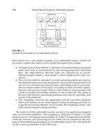
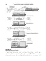
These concepts contribute to our vision of a high-level design flow embod-
ied in an experimental design platform for heterogeneous SoC/SiP, shown
in Figure 19.2. The ultimate goal is to enable the concurrent handling of
hardware/software and AMS/MT components in architectural exploration.
As shown in Figure 19.2, there is a clear bridge between system-level and
physical-level (or domain-specific) phases of design—in our view this bridge
System-level IP repository
System
model
HW+SW
+AMSMT
data
models
Domain-specific IP repository
User Cockpit Autopilot
Power
Robustness
Feasibility
Cost
Estimate
Performance
Power
Timing
Variability
Placement
Analyze
HW
AMSMT
SW
Interconnect
Packaging
Optimize
Function
Domain
Specifications
Define
FIGURE 19.2
Target SoC/SiP design flow.
Nicolescu/Model-Based Design for Embedded Systems 67842_C019 Finals Page 612 2009-10-14
612 Model-Based Design for Embedded Systems
is critical to setting up a continuum of abstraction levels between system and
physical design, enabling detailed analysis of cross-domain tradeoffs and
the correct balancing of constraints over the various domains, and hence the
achievement of optimally designed heterogeneous systems. The main impact
would be to combat the current inefficiency in design processes between (1)
the apriorigeneration of component specification sets at the system level in
the presence of uncertainty concerning the feasibility of these sets in the tar-
get technology and (2) the a posteriori evaluation of the differences between
specified and real component performance levels, generated at the physical
level in the presence of uncertainty of their impact and potential degrees of
freedom available at the system level. Learning systems can of course capi-
talize on the repeated use of estimation, optimization, and analysis to refine
the accuracy of predictions.
A typical example of where such exploration would be required is in
the optical interconnect demonstrator: based on software application con-
straints, system optimization requires the analysis of tradeoffs between (for
example) (1) the number of cores (and parallel software tasks) that can be
linked efficiently by optical interconnect to reduce the power contribution
of the data processing part of the application and (2) the technology char-
acteristics leading to a specific data rate/power ratio and the power con-
tribution of the data communication part of the application. Hence such
design technology can also be viewed as a high-level guide for design
management.
In this section, we will first focus on a preliminary definition of abstrac-
tion levels and how they fit into a model for the design process. We will
then consider the various elements pertaining to heterogeneous components
required for the design process at various abstraction levels, and formalize
this in a model for synthesizable AMS/MT IP, which we then show how to
implement in UML/XML.
19.2.1 Abstraction Levels
The concept of abstraction levels is one that must be addressed for heteroge-
neous SoC/SiP. Valid abstraction (i.e., when there is a clear and explicit path
to simplify representation at a higher level for all considered objects) is diffi-
cult to achieve when tightly coupled physical phenomena are present in the
system—this is the case even for digital electronics at nanometric technol-
ogy nodes, and the rise in AMS, RF, and heterogeneous content to address
future application requirements compounds this problem. Efficient ways
must be found to incorporate nondigital objects into design flows in order
to ultimately achieve AMS/RF/heterogeneous/digital hardware/software
codesign.
While hierarchy in the digital domain is based on the levels of signal
abstraction, AMS/MT hierarchy is typically based on structural decompo-
sition. It is necessary to combine and represent both types of hierarchy for
Nicolescu/Model-Based Design for Embedded Systems 67842_C019 Finals Page 613 2009-10-14
Platform for Model-Based Design of Integrated Multi-Technology Systems 613
Structural decomposition
Structural aggregation
m: Higher structural level
n: Lower structural level
Xy: Child block ID
Top-down
propagation
Bottom-up
extraction
w: Higher abstraction level
n: Lower abstraction level
Mobility through abstraction levels
Circuit
Structural decomposition and aggregation
0_A
f
0_A
s
0_A
b
0_A
c
1_A
f
2_A
f
2_A
s
2_A
b
2_B
b
2_B
s
2_B
f
2_C
f
2_C
s
2_C
b
2_A
c
2_B
c
2_C
c
1_A
s
1_A
b
Block
System
1_B
b
1_B
s
1_B
f
1_A
c
1_B
c
T01Bf
T01Af
Ny: Structural block ID
Tfs0A
Tfs1A
Tfs1B
T12Bf
T12Cf
T12Cs
T12Cb
T12Cc
T12Af
T12Bf
T12As
T12Bb
T12Bc
T12Ac
T12Ab
Tsb1B
Tbc1B
Tbc2A
TwxNy
TmnXy
Tbc2B
Tsb2B
Tfs2B
Tfs2C
Tsb2C
Tbc2C
Tsb2A
Tfs2A
Tsb1A
Tbc1A
Tsb0A
Tbc0A
T01Ac
T01Bc
T01Ab
T01Bb
T01As
T01Bs
Function
FIGURE 19.3
Modeling abstraction and structural hierarchies.
heterogeneous synthesis processes: hierarchy based on levels of abstraction,
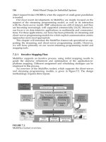
and hierarchy based on structural decomposition. Figure 19.3 shows a Petri
net style diagram [GIR2002] where the ovals (places) represent IP blocks
with various levels of abstraction (F, functional/mathematical; S, system; B,
block; C, circuit/component). A loose association between these levels and
existing modeling languages can be established: MATLAB
R
∗
/Simulink
R
†
for the top two levels; Verilog-AMS for the block level; and SPICE/Spectre
for the circuit/component level. In the diagram, the boxes situated on arcs
between places at different abstraction levels represent transitions, and indi-
cate the processes used to move between abstraction levels while preserving
the properties of each block’s functionality.
Structural decomposition can be represented by a set of transitions from
one block to several other blocks (usually at the same abstraction level) and
is also represented in Figure 19.3. For example, 0_A is the overall system to
be designed and is comprised of components 1_A and 1_B. 1_B can be fur-
ther decomposed into 2_A, 2_B, and 2_C. As can be seen from the diagram,
some places (with dotted lines) are not accessible: at the functional level, this
concerns 2_{A,B,C}
f
and illustrates the nonrepresentativity of strong physical
∗
/>†
/>Nicolescu/Model-Based Design for Embedded Systems 67842_C019 Finals Page 614 2009-10-14
614 Model-Based Design for Embedded Systems
coupling between IP blocks at this abstraction level; and at the circuit level, it
concerns 0_A
c
, illustrating the nonsimulability of the overall system at circuit
level.
It is worth noting that while single direction transitions are the usual rep-
resentation in this type of diagram, we have for simplicity here merged both
structural transitions (decomposition and aggregation) and abstraction level
transitions (top-down propagation, or “refinement,” and bottom-up extrac-
tion, or “abstraction”).
This approach enables clarification of the available/necessary steps in
the design process. It is quite clear that several routes exist to achieve com-
plete top-down synthesis of each individual component in the system, and
conversely several routes enable the bottom-up validation of the whole (the
top-down and bottom-up routes do not necessarily pass through the same
places).
19.2.1.1 Model for Synthesizable AMS/MT IP
Most analog and RF circuits are still designed manually today, resulting
in long design cycles and increasingly apparent bottlenecks in the overall
design process [GIE2005]. This explains the growing awareness in indus-
try that the advent of AMS/MT synthesis and optimization tools is a nec-
essary step to increase design productivity by assisting or even automating
the AMS/MT design process. The fundamental goal of AMS/MT synthesis
is to generate quickly a first-time-correct sized circuit schematic from a set
of circuit specifications. This is critical since the AMS/MT design problem is
typically under-constrained with many degrees of freedom and with many
interdependent (and often conflicting) performance requirements to be taken
into account.
Synthesizable (soft) AMS IP [HAM2003] extends the concept of digital
and software IP to the analog domain. It is difficult to achieve because the
IP hardening process (moving from a technology-independent, structure-
independent specification to a qualified layout of an AMS/MT block) relies
to a large extent on the quality of the tools being used to do this. It is our belief
that a clear definition of AMS/MT IP is an inevitable requirement to pro-
vide a route to system-level synthesis incorporating AMS/MT components.
Table 19.3 summarizes the main facets necessary to AMS/MT IP, where each
constituent element of design information is identified and the role of each is
described.
Figure 19.4 shows how these various facets of AMS/MT IP should be
brought together in an iterative single-level synthesis loop. This represents
“structural” decomposition transitions. First, the set S of the performance
criteria, originating from the higher hierarchical structural level n + 1in
Figure 19.4, is used to quantify how the IP block should carry out the
defined function. Performance criteria are composed of functional specifi-
cations and performance specifications: for example in an amplifier, S will
Nicolescu/Model-Based Design for Embedded Systems 67842_C019 Finals Page 615 2009-10-14
Platform for Model-Based Design of Integrated Multi-Technology Systems 615
TABLE 19.3
AMS/MT IP Block Facets
Property Short Description
Function definition Class of functions to which the IP block
belongs.
Performance criteria set S Quantities necessary to specify and to
evaluate the IP block.
Terminals Input/output links to which other IP
blocks can connect.
Structure Internal component-based structure of the
IP block.
Design variable set V List of independent design variables to be
used by a design method or optimization
algorithm.
Physical parameter set P List of physical parameters associated
with the internal components.
Evaluation method
∗
e Code defining how to evaluate the IP
block, that is, transform physical
parameter values to performance criteria
values. Can be equation or simulation
based (the latter requires a parameter
extraction method).
Parameter extraction method Code defining how to extract
performance criteria values from
simulation results (simulation-based
evaluation methods only).
Synthesis method
∗
m Code defining how to synthesize the IP
block, that is, transform performance
criteria requirements to design variable
values. Can be procedure- or
optimization based.
Constraint distribution method
∗
c Code defining how to transform IP block
parameters to specifications at a lower
hierarchical level.
contain gain (the single functional specification), bandwidth, power supply
rejection ratio, offset, etc. They have two distinct roles, related to the state of
the IP block in the design process.
• As block parameters when the IP block is a component of a larger
block, higher up in the hierarchy, in the process of being designed. In
this case it can be varied and must be constrained to evolve within a
given design space, i.e., s
low_i
< s
i
< s
high_i
.
• As specifications when the IP block is the block in the process of being
designed (such as here). In this case the value s
i
is a fixed target and
will be used to drive the design process through comparison with real
performance values s
ri
. Several possibilities exist to construct an error
function ε, the most common being a sum of n (the size of S) weighted