Model-Based Design for Embedded Systems- P62 docx
Bạn đang xem bản rút gọn của tài liệu. Xem và tải ngay bản đầy đủ của tài liệu tại đây (322.93 KB, 10 trang )
Nicolescu/Model-Based Design for Embedded Systems 67842_C018 Finals Page 596 2009-10-1
596 Model-Based Design for Embedded Systems
not provide means to describe new primitive modules, and thus no con-
verter ports can be used, converter modules are provided (ELN, LSF). The
motivation for providing a basic set of predefined converters is that replac-
ing single blocks of a TDF cluster with structure or even interface-accurate
models leads to a heterogeneous structure that combines
• TDF (and embedded transfer functions) for the executable specification
• LSF signals (or ELN nodes) for analog implementation
• SystemC DE signals for digital implementation
• TDF with bit-true data type for DSP SW implementation
The potential use of SystemC AMS modules (and thus converter ports,
converter modules) in hierarchical models as well as in hierarchical chan-
nels motivates a more sophisticated support for the design refinement of
structure.
18.3.4 Methodology-Specific Support in a Methodology-
Specific Library
Although SystemC AMS provides a basic set of converters, a richer and more
flexible set of converters is useful for design refinement, especially in the
case of structure refinement, where a functional (or computation accurate)
block is replaced with an interface and structure accurate block. In this case,
the MoC often differ from the originally used TDF model of computation.
Although in all cases the basic set of converters allows the design engineer
to set up a valid model, some additional effort and changes to the overall
system structure are typically needed. However, these changes may violate
principles of refinement that require changes to be made in a local sense,
and with low effort This violation may occur in particular in case of struc-
tural refinement by integrating circuit level models into functional models:
In this case, a refinement step would require the design engineer to modify
the overall model by introducing converter modules or converter ports that
translate the functional semantics (e.g., data flow, signal flow) into physical
sizes of electrical nodes.
To relieve the design engineer of this awkward and error prone con-
version tasks, the concept of polymorphic signals has been developed [10],
and has been recently extended to a facility called “converter channel” [11].
Converter channels can automatically connect SystemC modules that are
modeled using different MoCs, such as the TDF MoC of the SystemC AMS
extensions, or the DE MoC that is native to SystemC, while also performing
data-type conversion. The idea of the converter channel is that the designer
declares the MoC and the data type of the module that writes to the con-
verter channel, as well as up to two additional data types for the modules
that read from this channel. The MoC of the reading modules can be deter-
mined automatically by the interface that is implemented by the respective
port.
Nicolescu/Model-Based Design for Embedded Systems 67842_C018 Finals Page 597 2009-10-1
Design Refinement of Embedded Mixed-Signal Systems 597
Module
MoC
1
Module
MoC
1
Module
MoC
1
Module
MoC
2
Module
MoC
2
Module
MoC
3
Converter
Data type DT
1
Data type DT
2
Data type DT
1
Data type DT
1
Data type DT
1
Data type DT
3
Input signal
Output signal
3
Output signal
2
Output signal
1
MoC
1
MoC
1
DT
1
DT
2
Converter
MoC
1
MoC
2
DT
1
DT
1
Converterchannel < MoC
1
, DT
1
, DT
2
, DT
3
>
Converter
MoC
1
MoC
3
DT
1
DT
3
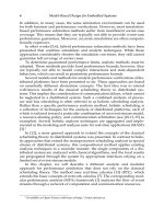
FIGURE 18.6
Internal structure of a converter channel connected to multiple reading
modules.
The converter channel then instantiates the appropriate signal(s) for the
writing module and the reading module(s), together with converter modules
that do the actual conversion work (see Figure 18.6). In the case of TDF→DE
conversion, for example, the respective converter module will utilize the con-
verter port described above. If the data types are different, the converter
module will also perform the data-type conversion. As an option, the con-
verter channel can also scale the input data, for example when converting
double values to data types such as sc_uint<n>. In this case, the user
passes the expected input range to the converter channel, such that this range
is scaled to the natural range of the target data type, while clipping every
input data out of bounds. Therefore, the converter channel can completely
replace the simple A/D converter from Example 18.2.
Besides the conversion work, the converter channel can also be used for
“integration validation.” It can check, for example, if a DE input is under
sampled when converting to TDF, which can occur if the DE input changes
more frequently compared to the sample rate of the TDF reader. Also, the
converter channel can check and handle some corner cases in process net-
work (PN) ↔ TDF conversion (see [11]). Finally, data type conversion issues
such as overflow are detected.
18.4 Simple Example for a Refinement Step Using
Converter Channels
In this section, we present an example that illustrates a single refine-
ment step in the design of a software defined radio (SDR). An overview
Nicolescu/Model-Based Design for Embedded Systems 67842_C018 Finals Page 598 2009-10-1
598 Model-Based Design for Embedded Systems
Sine
rf_in
Mixer
Mixedsig
Converter channel
Lowpass
(TDF or ELN)
Demodulate_an
Network (ELN)
or behavioral
model (TDF)
Software (DE or PN)
Demodulate_sw
1p_out
1
3
2
4
TDF-signal
FIGURE 18.7
A refinement example: SW-defined radio.
of a simple SDR system is shown in Figure 18.7. The RF input signal
is mixed with a sine wave of the same frequency as the carrier signal
and the result is processed by a lowpass filter. After that, the demodu-
lation follows. For demodulation, different realizations are possible: The
most power efficient implementation is pure hardware (A/D) and the
most flexible one considering support for different standards is the pure
software realization. Usually, a compromise between these two realiza-
tions has to be found considering flexibility, accuracy/bit width/bit error
rate (BER), power consumption, and required computing performance
(costs). The evaluation of the architecture variants necessitates the study
of an overall system. Starting with a pure functional model, a refinement
step could, for example, replace the TDF modulator with a model using
the DE MoC. More general, the A/D/SW partitioning could be altered
successively and the results could be compared until evaluation yields
acceptable results. These refinement steps can be modeled efficiently using
converter channels because they automatically adopt data types and model
of computation.
As a simple example for some refinement steps, we use the simple SDR
concept as illustrated by Figure 18.7. The input of the software demodulator
is an integer with fixed bit width. Example 18.3 shows the corresponding
top-level SystemC code using two converter channels.
bitwidth=8;
sca_tdf::sca_signal<double> rf_in; // incoming RF-signal
sca_tdf::sca_signal <double> sine; // sine waverf_in
converterchannel<TDF, double> mixedsig;
// RF-signal multiplied with sine-wave
converterchannel<TDF,double, sc_int<bitwidth>>lp_out;
// output of lp-filter
lp_out.setRangeScaling( -1. , 1. ); // assuming the
value range within [-1,1]
Nicolescu/Model-Based Design for Embedded Systems 67842_C018 Finals Page 599 2009-10-1
Design Refinement of Embedded Mixed-Signal Systems 599
mixer mix("mix"); // mixes the two input signals
mix.in1(rf_in);
mix.in2(sine);
mix.out(mixedsig);
lowpass_behavioural lp("lp"); // lowpass filter, either
T-SDF-module
lp.in(mixedsig); // or electrical network
lp.out(lp_out);
demodulate_sw dem_sw("dem_sw", bitwidth); // software
demodulator with
dem_sw.in(lp_out); // sc_int<bitwidth> input
demodulate_an dem_an("dem_an"); // analogue demodulator
dem_an.in(lp_out);
Example 18.3 SW-defined radio with converter channels Regarding design space
exploration and mixed level simulation, this example gives rise to the following tasks
(the numbers refer to those in Figure 18.7):
1. Realizing the lowpass filter either as a (behavioral) TDF-module or as an elec-
trical network.
2. Realizing the software demodulator either as a PN or as a DE module.
3. Varying the bit width of the input of the software demodulator.
4. Realizing the analog demodulator either as a (behavioral) TDF-module or as an
electrical network.
To further complicate matters, any subset of these tasks can be performed in
parallel. It is clear that the effort for manually inserting (and adapting) the
appropriate converters would be significant. For example, assume an initial
model with the lowpass filter and the analog demodulator modeled as TDF
modules and the software demodulator modeled within the PN MoC, taking
sc_int<bitwidth> inputs. We then would need a TDF→PN converter from
the output of the lowpass filter to the software modulator, which would also
convert double values to sc_int<bitwidth> values. Now, executing the tasks
above would require the following manual conversion steps (in addition to
the design of ELN modules itself):
1. Realizing the lowpass filter as an electrical network:
I. Insert a TDF→ELN converter between the mixer and the low-
pass filter.
II. Replace the initial TDF→DE converter by an ELN→DE con-
verter, which also converts physical sizes in double precision
to sc_int<bitwidth>.
III. Instantiate appropriate signals to connect the TDF→ELN con-
verter with the ELN→KPN converter.
2. Realizing the software demodulator as a DE module: Replace the ini-
tial TDF→DE converter by a TDF→DE converter, which also converts
Nicolescu/Model-Based Design for Embedded Systems 67842_C018 Finals Page 600 2009-10-1
600 Model-Based Design for Embedded Systems
double to sc_int<bitwidth>. Note, that using a SystemC AMS converter
port makes no sense here since the analog demodulator is still in the
TDF domain. Instantiate appropriate signals to connect them.
3. Varying the bit width of the input of the software demodulator: Change
the output of the TDF→DE converter and the type of the signal that
connects it to the software demodulator to sc_int<new_bitwidth>.The
data-type conversion algorithm of the converter must also be altered
slightly. Note, that a converter that takes the bitwidth as parameter
would alleviate the design effort.
4. Realizing the analog demodulator as an electrical network: Insert a
TDF→ELN converter between the lowpass filter and the analog demod-
ulator. Instantiate an appropriate signal to connect them.
Obviously, steps 1–4 are a significant effort for a design engineer and there-
fore are against the principle of interactive, iterative refinement. By using
converter channels, however, the code for each of the possible variants
would be very similar to the code in Example 18.3. The value of the variable
bitwidth would change as well as the class names of the respective mod-
ules (e.g., changing lowpass_behavioral to lowpass_electrical). This simple
example shows the convenience that converter channels offer to the design
engineer.
18.5 Conclusion and Outlook
With the AMS extensions, SystemC becomes amenable to modeling HW/SW
systems and—at functional and architecture level—analog and mixed-signal
subsystems. The intended use cases include executable specification, archi-
tecture exploration, virtual prototyping, and integration validation. We have
described a methodology that efficiently uses the AMS extensions together
with the newly introduced converter channels. To support it the concept of a
converter channel has been introduced.
It is desirable to incorporate an even more abstract view into the method-
ology, namely Transaction Level Modeling (TLM) [2], which allows design
engineers to perform abstract modeling, simulation, and design of HW/SW
system architectures. The idea of TLM is to abstract away the low-level
events occurring in bus communication into a singledata object called “trans-
action,” that is passed from process to process by method calls. TLM not only
enables early software development, but also enhances simulation perfor-
mance. Recently, the OSCI released the TLM 2.0 standard [13], and an exten-
sion library with facilities for TLM (mainly method interfaces and a standard
transaction object, the “generic payload”). Parts of the standard are cod-
ing guidelines for different coding styles. Especially the “loosely timed cod-
ing” style contains state of the art simulation techniques for fast simulation.
Nicolescu/Model-Based Design for Embedded Systems 67842_C018 Finals Page 601 2009-10-1
Design Refinement of Embedded Mixed-Signal Systems 601
By allowing processes to run ahead of global simulation time (temporal
decoupling) locally, context switches can be reduced, which increases sim-
ulation performance, possibly for the price of a lower simulation accuracy.
In [14], an early approach was presented to couple loosely timed TLM
models with models using the AMS extensions. It was shown that the loosely
timed modeling style of TLM 2.0 can be exploited efficiently to fit with the
AMS extensions TDF MoC, preserving the high simulation performance of
both the simulation approaches. The key idea there emerged from the obser-
vation that TDF processes also run ahead of the SystemC simulation time
(see Figure 18.4). Therefore, it is possible to set up converters that incorpo-
rate both temporal decoupling effects as well as trigger synchronization only
when needed. With an efficient TLM-AMS extensions coupling available,
the first step is implemented for an integrated E-AMS systems refinement
approach using TLM and AMS extensions.
References
1. IEEE Std. 1666–2005. IEEE Press, New York.
2. F. Ghenassia (editor), Transaction Level Modeling with SystemC, Springer,
Dordrecht, the Netherlands, 2005.
3. The MathWorks
R
Simulink
R
, />simulink
4. J. Eker, J. W. Janneck, E. A. Lee, J. Liu, X. Liu, J. Ludvig, S. Neuendorffer,
S. Sachs, and Y. Xiong, Taming heterogeneity—the Ptolemy approach,
Proceedings of the IEEE, v.91, No. 1, pp. 127–144, January 2003.
5. IEEE Std. 1076.1-2007. IEEE Press, New York.
6. Accellera: Verilog-AMS Language Reference Manual Version 2.2,
2004. Analog & Mixed-Signal Extensions to Verilog HDL;
/>7. OSCI AMS Working Group, SystemC AMS extensions Requirements Speci-
fication, 2007.
8. A. Vachoux, C. Grimm, and K. Einwich, SystemC extensions for hetero-
geneous and mixed discrete/continuous systems. In: International Sym-
posium on Circuits and Systems 2005 (ISCAS ’05), Kobe, Japan, May 2005.
IEEE Press, New York.
9. C. Grimm, Modeling and refinement of mixed signal systems with
SystemC. In: SystemC: Methodologies and Applications, Kluwer Academic
Publisher (KAP), Norwell, MA, June 2003.
Nicolescu/Model-Based Design for Embedded Systems 67842_C018 Finals Page 602 2009-10-1
602 Model-Based Design for Embedded Systems
10. R. Schroll, Design komplexer heterogener Systeme mit Polymorphen
Signalen. PhD thesis, Institut für Informatik, Universität Frankfurt,
Germany, 2007.
11. M. Damm, F. Herrera, J. Haase, E. Villar, and C. Grimm, Using converter
channels within a top-down design flow in SystemC. In: Proceedings of
the Austrochip 2007, Graz, Austria, 2007.
12. C. Grimm, M. Barnasconi, A. Vachoux, and K. Einwich, An introduc-
tion to modeling embedded analog/mixed-signal systems using Sys-
temC AMS extensions. OSCI, June 2008. www.systemc.org
13. Open SystemC Initiative. OSCI TLM2.0 standard, June 2008.
14. M. Damm, C. Grimm, J. Haase, A. Herrholz, and W. Nebel, Connecting
Systemc-AMS models with OSCI TLM 2.0 models using temporal decou-
pling. In: Proceedings of the Forum on Specification and Design Languages
(FDL), Stuttgart, Germany, 2008.
15. N. Wirth, Program development by stepwise refinement. Communica-
tions of the ACM, 14 (1971), S. 221–227.
16. J. Romberg and C. Grimm, Refinement of hybrid systems from formal
models to design languages. In C. Grimm (editor), Languages for System
Specification, Kluwer Academic Publisher: Dordrecht, Boston, New York,
London, 2004.
17. M. Fowler, Refactoring: Improving the Design of Existing Code, Addison-
Wesley, London.
Nicolescu/Model-Based Design for Embedded Systems 67842_C019 Finals Page 603 2009-10-14
19
Platform for Model-Based Design of
Integrated Multi-Technology Systems
Ian O’Connor
CONTENTS
19.1 Rationale for Multi-Technology Design Exploration 603
19.2 Rune
II
Platform 608
19.2.1 Abstraction Levels 612
19.2.1.1 Model for Synthesizable AMS/MT IP 614
19.2.2 UML/XML Implementation 618
19.3 Multi-Technology Design Exploration Application: Integrated
OpticalInterconnect 622
19.3.1 Models for the Simulation and Synthesis of an Optical Link 622
19.3.2 Optical Point-to-Point Link Synthesis 623
19.3.3 Performance Metrics and Specification Sets 630
19.4 Integrated Optical Interconnect Investigation Program and Results 631
19.4.1 Gate Area Analysis 632
19.4.2 Delay Analysis 632
19.4.3 Power Analysis 634
19.5 Conclusions and Ideas for the Future 638
Acknowledgment 640
References 640
19.1 Rationale for Multi-Technology Design Exploration
Until recently, the single recognized vector enabling the improvement of the
silicon system performance was perceived to be the progressive reduction
(scaling) in CMOS device dimensions. Popularly known as Moore’s law, this
trend will lead to the emergence of transistors of physical gate lengths of
10–18 nm in the 2010–2015 timeframe, according to the predictions of the
ITRS.
∗
Consequently, the complexity of systems on chip (SoC) will reach
unprecedented levels (high-performance microprocessors already contain
over 10
9
transistors). However, the pursuit of Moore’s law through scal-
ing will meet significant future, intrinsic device hurdles (such as leakage,
∗
International Technology Roadmap for Semiconductors ( />603
Nicolescu/Model-Based Design for Embedded Systems 67842_C019 Finals Page 604 2009-10-14
604 Model-Based Design for Embedded Systems
interconnect, static power, quantum effects) to the capability of realizing
system architectures using CMOS transistors with the performance lev-
els required by future applications. It is recognized that these limitations,
as much fundamental as economic, require the semiconductor industry to
explore the use of novel devices able to complement or even replace the
CMOS transistor in SoC within the next decade.
Hence, from the miniaturization of existing systems (position sensors, labs
on chip, etc.) to the creation of specific integrated functions (memory, radio
frequency (RF) tuning, energy, etc.), nanoscale and nonelectronic devices are
being integrated to create nanoelectronic and heterogeneous systems in pack-
age (SiP), SoC, and 3D integrated circuits. This approach for future systems
will have significant impact on several economic sectors, and is driven by
• The need for the miniaturization of existing systems to benefit from
technological advances and improve performance at lower overall cost
• The potential replacement of specific functions in SoC/SiP with
nanoscale or nonelectronic devices (nanoswitches, optical interconnect,
magnetic memory, etc.)
• The advent of high-performance user interfaces (virtual surgical oper-
ations, games consoles, etc.)
• The rise of low-power mobile systems (communications and mobile
computing) and wireless sensor networks for the measurement of phe-
nomena inaccessible to single-sensor systems
In fact, the maturity and necessary diversification of integration technologies
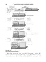
mean that three research directions are now open, as shown in Figure 19.1,
an extended version of ENIAC
∗
’s vision: “More Moore” (continued scaling);
“More than Moore” (diversification); “Beyond Moore” (alternative devices).
While “More Moore” focuses on the pursuit of traditional scaling for com-
putation, “More than Moore” enables interaction with the real world and
also system performance improvement through “equivalent” scaling with
unconventional devices. It is clear that future SoC will be based on increas-
ingly complex and diversified integration technologies in order to achieve
unprecedented levels of functionality.
While the general benefits of heterogeneous integration appear to be
clear, this evolution represents a strong paradigm shift for the semiconductor
industry. This shift toward diversification and away from the scaling trend
that has lasted over 40 years is possible because the integration technology
(or at least the individual technological steps) exists to do so [ROO2005].
However, the capacity to translate system drivers into technology require-
ments (and consequently guidance for investment) to exploit such diversi-
fication is severely lacking. Such a role can only be fulfilled by a radical
shift in design technology to address the new and vast problem of hetero-
geneous system design while remaining compatible with standard “More
∗
European Nanoelectronics Initiative Advisory Council ( />Nicolescu/Model-Based Design for Embedded Systems 67842_C019 Finals Page 605 2009-10-14
Platform for Model-Based Design of Integrated Multi-Technology Systems 605
System technologies
Baseline
CMOS
Memory
More Moore More than Moore
Sense
interact
empower
Nondigital content
multilevel heterogeneous integration
(SiP or 3DSIC)
Physical heterogeneity
System miniaturisation (wireless
sensor networks, ambient
intelligence, labs on chip, etc.)
specific functions (MEMS resonators,
optical interconnect, etc.)
Compute
store
Digital content
complex design
(SoC)
Evolutionary
technologies,
massive complexity
MoC and abstraction
level heterogeneity
RF Passives
HV
power
Sensors
actuators
Biological
fluidics
(a)
(b)
Design technologies
Architectural
improvement
vector
Multidomain
improvement
vector
Economic and
physical
obstacles
More Moore
technological and physical
constraints
Design
methods and tools
Complexity
RF and AMS
sensor and actuator
The function view
combining two worlds: HW and SW
yet with very different design
paradigms
+ HdSW
Reduced physical dimensionsFull system in a package
FIGURE 19.1
(a) ENIAC’s vision of future integration technology diversification in the
semiconductor industry. (b) The impact of technology diversification impact
on design technology. (Adapted from ENIAC (European Nanoelectronics
Initiative Advisory Council) SRA2007, .)