Model-Based Design for Embedded Systems- P39 ppsx
Bạn đang xem bản rút gọn của tài liệu. Xem và tải ngay bản đầy đủ của tài liệu tại đây (235.85 KB, 10 trang )
Nicolescu/Model-Based Design for Embedded Systems 67842_C011 Finals Page 346 2009-10-2
346 Model-Based Design for Embedded Systems
the core to the iMesh on-chip network. The combination of a core and a
switch form the basic building block of the Tilera Processor: the tile. Each
core is a fully functional processor capable of running complete operating
systems and off-the-shelf “C” code. Each core is optimized to provide a high
performance/power ratio, running at speeds between 600 MHz and 1 GHz,
with power consumption as low as 170 mW in a typical application. Each
core supports standard processor features such as
• Full access to memory and I/O
• Virtual memory mapping and protection (MMU/TLB)
• Hierarchical cache with separate L1-I and L1-D
• Multilevel interrupt support
• Three-way VLIW pipeline to issue three instructions per cycle
The cache subsystem on each tile consists of a high-performance, two-
level, non-blocking cache hierarchy. Each processor/tile has a split level 1
cache (L1 instruction and L1 data) and a level 2 cache, keeping the design,
fast and power efficient. When there is a miss in the level 2 cache of a spe-
cific processor, the level 2 caches of the other processors are searched for the
data before external memory is consulted. This way, a large level 3 cache is
emulated.
This promotes on-chip access and avoids the bottleneck of off-chip global
memory. Multicore coherent caching allows a page of shared memory,
cached on a specific tile, to be accessed via load/store references to other
tiles. Since one tile effectively prefetches for the others, this technique can
yield significant performance improvements.
To fully exploit the available compute power of large numbers of pro-
cessors, a high-bandwidth, low-latency interconnect is essential. The net-
work (iMesh) provides the high-speed data transfer needed to minimize
system bottlenecks and to scale applications. iMesh consists of five distinct
mesh networks: Two networks are completely managed by hardware and
are used to move data to and from the tiles and memory in the event of
cache misses or DMA transfers. The three remaining networks are available
for application use, enabling communication between cores and between
cores and I/O devices. A number of high-level abstractions are supplied for
accessing the hardware (e.g., socket-like streaming channels and message-
passing interfaces.) The iMesh network enables communication without
interrupting applications running on the tiles. It facilitates data transfer
between tiles, contains all of the control and datapath for each of the net-
work connections, and implements buffering and flow control within all the
networks.
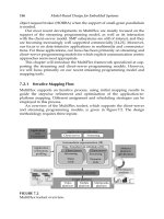
11.3.4.1 Design Methodology
The TILE64 processor is programmable in ANSI standard C and C++. Tiles
can be grouped into clusters to apply the appropriate amount of processing
power to each application and parallelism can be explicitly specified.
Nicolescu/Model-Based Design for Embedded Systems 67842_C011 Finals Page 347 2009-10-2
Reconfigurable MultiCore Architectures 347
11.4 Conclusion
In this chapter, we addressed reconfigurable multicore architectures for
streaming DSP applications. Streaming DSP applications express computa-
tion as a data flow graph with streams of data items (the edges) flowing
between computation kernels (the nodes). Typical examples of streaming
DSP applications are wireless baseband processing, multimedia processing,
medical image processing, and sensor processing. These application domains
require flexible and energy-efficient architectures. This can be realized with a
multicore architecture. The most important criteria for designing such a mul-
ticore architecture are predictability and composability, energy efficiency,
programmability, and dependability. Two other important criteria are per-
formance and flexibility. Different types of processing cores have been dis-
cussed, from ASICs, reconfigurable hardware, to DSPs and GPPs. ASICs
have high performance but suffer from poor flexibility while DSPs and GPPs
offer flexibility but modest performance. Reconfigurable hardware combines
the best of both worlds. These different processing cores are, together with
memory- and I/O blocks assembled into MP-SoCs. MP-SoCs can be clas-
sified into two groups: homogeneous and heterogeneous. In homogeneous
MP-SoCs, multiple cores of a single type are combined whereas in a hetero-
geneous MP-SoC, multiple cores of different types are combined.
We also discussed four different architectures: the M
ONTIUM/ANNABELLE
SoC, the Aspex Linedancer, the PACT-XPP, and the Tilera processor. The
M
ONTIUM, a coarse-grain, run-time reconfigurable core has been used as one
of the building blocks of the A
NNABELLE SoC. The ANNABELLE SoC can be
classified as a heterogeneous MP-SoC. The Aspex Linedancer is a homoge-
neous MP-SoC where a single instruction is executed by multiple processors
simultaneously (SIMD). The PACT-XPP is an array processor where multi-
ple ALUs are combined in a 2D structure. The Tilera processor is an example
of a homogeneous MIMD MP-SoC.
References
1. The International Technology Roadmap for Semiconductors, ITRS
Roadmap 2003. Website, 2003. />Home2003.htm.
2. A coarse-grained reconfigurable architecture template and its compi-
lation techniques. PhD thesis, Katholieke Universiteit Leuven, Leuven,
Belgium, January 2005.
3. Nvidia g80, architecture and gpu analysis, 2007.
Nicolescu/Model-Based Design for Embedded Systems 67842_C011 Finals Page 348 2009-10-2
348 Model-Based Design for Embedded Systems
4. Aspex Semiconductor: Technology. Website, 2008. ex-
semi.com/q/technology.shtml.
5. Mimagic 6+ Enables Exciting Multimedia for Feature Phones. Web-
site, 2008. />Brief.pdf/.
6. PACT. 2008.
7. Tilera Corporation. 2008.
8. Atmel Corporation. ATC13 Summary. , 2007.
9. A. Banerjee, P.T. Wolkotte, R.D. Mullins, S.W. Moore, and Gerard J.M.
Smit. An energy and performance exploration of network-on-chip archi-
tectures. IEEE Transactions on Very Large Scale Integration (VLSI) Systems,
17(3): 319–329, March 2009.
10. V. Baumgarte, G. Ehlers, F. May, A. Nückel, M. Vorbach, and M. Wein-
hardt. PACT XPP—A self-reconfigurable data processing architecture.
Journal of Supercomputing, 26(2):167–184, September 2003.
11. M.D. van de Burgwal, G.J.M. Smit, G.K. Rauwerda, and P.M. Heysters.
Hydra: An energy-efficient and reconfigurable network interface. In Pro-
ceedings of the International Conference on Engineering of Reconfigurable Sys-
tems and Algorithms (ERSA’06), Las Vegas, NV, pp. 171–177, June 2006.
12. G. Burns, P. Gruijters, J. Huisken, and A. van Wel. Reconfigurable
accelerator enabling efficient sdr for low-cost consumer devices. In SDR
Technical Forum, Orlando, FL, November 2003.
13. A.P. Chandrakasan, S. Sheng, and R.W. Brodersen. Low-power cmos
digital design. IEEE Journal of Solid-State Circuits, 27(4):473–484, April
1992.
14. W.J. Dally, U.J. Kapasi, B. Khailany, J.H. Ahn, and A. Das. Stream pro-
cessors: Progammability and efficiency. Queue, 2(1):52–62, 2004.
15. European Telecommunication Standard Institute (ETSI). Broadband Radio
Access Networks (BRAN); HIPERLAN Type 2; Physical (PHY) Layer,ETSI
TS 101 475 v1.2.2 edition, February 2001.
16. Y. Guo. Mapping applications to a coarse-grained reconfigurable archi-
tecture. PhD thesis, University of Twente, Enschede, the Netherlands,
September 2006.
17. P.M. Heysters, L.T. Smit, G.J.M. Smit, and P.J.M. Havinga. Max-log-map
mapping on an fpfa. In Proceedings of the 2005 International Conference
on Engineering of Reconfigurable Systems and Algorithms (ERSA’02),Las
Vegas, NV, pp. 90–96, June 2002. CSREA Press, Las Vegas, NV.
Nicolescu/Model-Based Design for Embedded Systems 67842_C011 Finals Page 349 2009-10-2
Reconfigurable MultiCore Architectures 349
18. P.M. Heysters. Coarse-grained reconfigurable processors – flexibility
meets efficiency. PhD thesis, University of Twente, Enschede, the
Netherlands, September 2004.
19. R.P. Kleihorst, A.A. Abbo, A. van der Avoird, M.J.R. Op de Beeck,
L. Sevat, P. Wielage, R. van Veen, and H. van Herten. Xetal: A low-power
high-performance smart camera processor. IEEE International Symposium
on Circuits and Systems, 2001. ISCAS 2001, 5:215–218, 2001.
20. PACT XPP Technologies . , 2007.
21. D.C. Pham, T. Aipperspach, D. Boerstler, M. Bolliger, R. Chaudhry,
D. Cox, P. Harvey et al. Overview of the architecture, circuit design, and
physical implementation of a first-generation cell processor. IEEE Journal
of Solid-State Circuits, 41(1):179–196, January 2006.
22. G.K. Rauwerda, P.M. Heysters, and G.J.M. Smit. Towards software
defined radios using coarse-grained reconfigurable hardware. IEEE
Transactions on Very Large Scale Integration (VLSI) Systems, 16(1):3–13,
January 2008.
23. Recore Systems. , 2007.
24. G. J. M. Smit, A. B. J. Kokkeler, P. T. Wolkotte, and M. D. van de Burgwal.
Multi-core architectures and streaming applications. In I. Mandoiu and
A. Kennings (editors), Proceedings of the Tenth International Workshop on
System-Level Interconnect Prediction (SLIP 2008), New York, pp. 35–42,
April 2008. ACM Press, New York.
25. S.R. Vangal, J. Howard, G. Ruhl, S. Dighe, H. Wilson, J. Tschanz, D. Finan
et al. An 80-tile sub-100-w teraflops processor in 65-nm cmos. IEEE Jour-
nal of Solid-State Circuits, 43(1):29–41, January 2008.
26. E. Waingold, M. Taylor, D. Srikrishna, V. Sarkar, W. Lee, V. Lee, J. Kim
et al. Baring it all to software: Raw machines. Computer, 30(9):86–93,
September 1997.
Nicolescu/Model-Based Design for Embedded Systems 67842_C011 Finals Page 350 2009-10-2
Nicolescu/Model-Based Design for Embedded Systems 67842_C012 Finals Page 351 2009-10-1
12
FPGA Platforms for Embedded Systems
Stephen Neuendorffer
CONTENTS
12.1 Introduction 351
12.2 Background 353
12.2.1 Processor Systems in FPGAs 353
12.2.2 FPGA Configuration and Reconfiguration 355
12.2.3 Partial Reconfiguration with Processors 358
12.2.4 Reusable FPGA Platforms for Embedded Systems 360
12.3 EDK Designs with Linux 361
12.3.1 Design Constraints 361
12.3.2 Device Trees 362
12.4 Introduction to Modular Partial Reconfiguration 363
12.5 EDK Designs with Partial Reconfiguration 364
12.5.1 Abstracting the Reconfigurable Socket 365
12.5.2 Interface Architecture 365
12.5.3 Direct Memory Access Interfaces 366
12.5.4 External Interfaces 368
12.5.5 Implementation Flow 369
12.6 Managing Partial Reconfiguration in Linux 370
12.7 Putting It All Together 372
12.8 Conclusion 375
References 377
12.1 Introduction
Increasingly, programmable logic (such as field programmable gate arrays
[FPGAs]) is a critical part of low-power and high-performance signal pro-
cessing systems. Typically, these systems also include a complex system
architecture, along with control processors, digital signal processing (DSP)
elements, and perhaps dedicated circuits. In some cases, it is economical
to integrate these system components in ASIC technology. As a result, a
wide variety of general purpose or application specific standard product
(ASSP) system-on-chip (SOC) architectures are available in the market. From
the perspective of a system designer, these architectures solve a large por-
tion of the system design problem, typically providing application-specific
351
Nicolescu/Model-Based Design for Embedded Systems 67842_C012 Finals Page 352 2009-10-1
352 Model-Based Design for Embedded Systems
I/O interfaces, an operating system for the control processor, processor
application programming interfaces (APIs) for accessing dedicated circuits,
or communicating with programmable elements such as DSP cores.
As FPGAs have become larger and more capable, it has become possi-
ble to integrate a large portion of the system architecture completely within
an FPGA, including control processors, communication buses, DSP process-
ing, memory, I/O interfaces, and application-specific circuits. For a system
designer, such a System-in-FPGA (SIF) architecture may result in better sys-
tem characteristics if an appropriate ASSP does not exist. At the same time,
designing using FPGAs eliminates the initial mask costs and process technol-
ogy risks associated with custom ASIC design, while still allowing a system
to be highly tuned to a particular application.
Unfortunately, designing a good SIF architecture from scratch and imple-
menting it successfully can still be a risky, time-consuming process. Given
that FPGAs only exist in fixed sizes, leveraging all the resources available
in a particular device can be challenging. This problem has become even
more acute given the heterogeneous nature of current FPGA architectures,
making it more important to trade off critical resources in favor of less criti-
cal ones. Furthermore, most design is still performed at the register-transfer
level (RTL) level, with few mechanisms to capture interface requirements or
guarantee protocol compatibility. Constructing radically new architectures
typically involves significant code rewriting and under practical design pres-
sures is not an option, given the time required for system verification.
Model-based design is one approach to reducing this risk. By focusing
on capturing a designer’s intention and providing high-level design con-
structs that are close to a particular application domain, model-based design
can enable a designer to quickly implement algorithms, analyze trade-offs,
and explore different alternatives. By raising the level of abstraction, model-
based design techniques can enable a designer to focus on key system-level
design decisions, rather than low-level implementation details. This process,
often called “platform-based design” [10,16], enables higher level abstrac-
tions to be expressed in terms of lower level abstractions, which can be more
directly implemented.
Unfortunately, in order to provide higher level design abstractions, exist-
ing model-based design methodologies must still have access to robust basic
abstractions and design libraries. Of particular concern in FPGA systems is
the role of the control processor as more complex processor programs, such
as an operating system, are used. The low-level interfaces between the pro-
cessor and the rest of the system can be fragile, since the operating system
and hardware must coordinate to provide basic abstractions, such as pro-
cess scheduling, memory protection, and power management. Architecting,
debugging, and verifying this interaction tends to require a wide span of
skills and specialized knowledge and can become a critical design problem,
even when using traditional design techniques.
One solution to this problem is to separate the control processor
subsystem from the bulk of the system and provide it as a fixed part of
Nicolescu/Model-Based Design for Embedded Systems 67842_C012 Finals Page 353 2009-10-1
FPGA Platforms for Embedded Systems 353
the FPGA platform. This subsystem can remain simple while being capable
of configuring and reconfiguring the FPGA fabric, bootstrapping an operat-
ing system, and providing a basis for executing application-specific control
code. Historically, several architectures have provided such a platform with
the processor system implemented in ASIC technology coupled with pro-
grammable FPGA fabric, including the Triscend architecture [20], which was
later acquired by Xilinx. Although current FPGAs sometimes integrate hard
processor cores (such as in the Xilinx Virtex 2 Pro family), a complete proces-
sor subsystem is typically not provided.
This chapter describes the use of the partial reconfiguration (PR) capabil-
ities of some FPGAs to provide a complete processor-based platform using
existing general-purpose FPGAs. PR involves the reconfiguration of part of
an FPGA (a reconfigurable region) while another part of the FPGA (a static
region) remains active and operating. Using PR, the processor subsystem
can be implemented as a largely application-independent static region of the
FPGA, while the application-specific portion can be implemented in a recon-
figurable region. The processor subsystem can be verified and optimized
beforehand, combined with an operating system image and distributed as
a binary image. From the perspective of a designer or a model-based design
tool, the static region of the FPGA becomes part of the FPGA platform, while
the reconfigurable region can then be treated as any other FPGA, albeit with
some resources reserved.
To understand the requirements for designing such a platform, we will
first provide some background of how processors and PR are used to design
SIF architectures. Then, we will describe the currently available tools, par-
ticularly related to PR, for building a reusable platform. Lastly, we will
provide an in-depth design example showing how such a platform can be
constructed.
12.2 Background
12.2.1 Processor Systems in FPGAs
Processor-based systems are commonly constructed in FPGAs. An obvious
way to build such a system is to take the RTL used for an ASIC implementa-
tion and target the RTL toward the FPGA using logic synthesis. In most cases,
however, the resulting FPGA design is relatively inefficient (being both rela-
tively large in silicon area and slow). Recent studies suggest that direct FPGA
implementation may be around 40 times larger (in silicon area) and one-third
of the clock speed of a standard-cell design on small benchmark circuits [9].
Experience with emulating larger processor designs, such as the Sparc V9
core from the OpenSparc T1 [19] and the PowerPC 405 core, in FPGAs sug-
gest a slowdown of at least 20 times compared to ASIC implementations.
Nicolescu/Model-Based Design for Embedded Systems 67842_C012 Finals Page 354 2009-10-1
354 Model-Based Design for Embedded Systems
The differences arise largely because of the overhead of FPGA pro-
grammability, which requires many more transistors than an equivalent
ASIC implementation. However, whereas many ASIC processors have com-
plex architectures in order to meet high computation requirements, systems
designed for FPGAs tend to make use of FPGA parallelism to meet the bulk
of the computation requirements. Hence, only relatively simple control pro-
cessors are necessary in FPGA systems, when combined with application-
specific FPGA design. When a processor architecture can be tuned to match
the FPGA architecture, as is typically done with “soft-core” processors, such
as the Xilinx Microblaze, reasonable clock rates ( 100 MHz) can be achieved
even in small, relatively slow, cost-optimized Xilinx Spartan 3 FPGAs. Alter-
natively, somewhat higher clock rates (up to 500 MHz) and performance
can be achieved by incorporating the processor core as a “hard-core” in the
FPGA, as is done with PowerPC cores in Xilinx Virtex 4 FX FPGAs.
One advantage of a faster control processor is being able to effectively run
larger, more complex control programs. Operating systems are often used to
mitigate this complexity. An operating system not only provides access to
various resources in the system, but also enables multiple pieces of indepen-
dent code to effectively share those resources by providing locking, memory
allocation, file abstractions, and process scheduling. In addition, operating
systems are designed to be robust and stable where an application process
cannot corrupt the operating system or other processes, making it signifi-
cantly easier to design and debug large systems.
Such an architecture, which combines a simple control processor hosting
an operating system with a high-performance computational engine, is not
unique to FPGA-based systems. With the move toward multicore architec-
tures in embedded processing platforms, typically one processor core serves
the role of the control processor. This processor typically boots first, and is
responsible for configuring and managing the main computational engine(s),
which are typically programmable processors tuned for a particular appli-
cation domain, such as signal processing or networking. Even in platforms
where the computational engines are specialized and not programmable pro-
cessors at the instruction level, such as in low-power cell phone platforms,
some initialization and coordination of data transfer must still be performed.
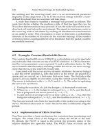
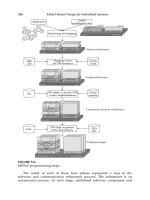
The variety in the possible architectures can be seen in Figure 12.1, which
summarizes the architecture of several embedded processing platforms.
Platform Application Control Proc. Data Proc.
IBM cell Media/computing 64-bit PPC 8 128-bit SIMD RISC
Nexperia PNX8526
Digital television MIPS 1 VLIW and dedicated
Intel IXP2800
Network processing XScale (ARMv5) 16 multithreaded RISC
TI OMAP2430
Cell phone handset ARM 1136 dedicated
FIGURE 12.1
Summary of some existing embedded processing platforms with control
processors.
Nicolescu/Model-Based Design for Embedded Systems 67842_C012 Finals Page 355 2009-10-1
FPGA Platforms for Embedded Systems 355
Regardless of the processor core architecture, the core must still be inte-
grated into a system in order to access peripherals and external memory.
Typically, most system peripherals and device interfaces are implemented in
the FPGA fabric, in order to provide the maximum amount of system flexi-
bility. For instance, the Xilinx embedded development kit (EDK) [24] enables
FPGA users to assemble existing processor and peripheral IP cores to design
a SIF architecture. Application-specific FPGA modules can be imported as
additional cores into EDK, or alternatively, the RTL generated by EDK can
be encapsulated as a blackbox inside a larger HDL design.
12.2.2 FPGA Configuration and Reconfiguration
FPGAs are designed primarily to implement arbitrary bit-oriented logic cir-
cuits. In order to do this, they consist primarily of “lookup tables” (LUTs)
for implementing the combinational logic of the circuit, “flip-flops” (FFs)
for implementing registers in the circuit, and programmable interconnect for
passing signals between other elements. Typically, pairs of LUTs and FFs are
grouped together with some additional combinational logic for efficiently
forming wide logic functions and arithmetic operations. The Xilinx Virtex 4
slice, which combines two LUTs and two FFs, is shown in Figure 12.2. In the
Virtex 4 architecture, four slices are grouped together with routing resources
in a single custom design called a configurable logic block (CLB). The layout
of FPGAs consists primarily of many tiles of the basic CLB, along with tiles
for other other elements necessary for a working system, such as embedded
memory (BRAM), external IO pins, clock generation and distribution logic,
and even processor cores.
In order to implement a given logic circuit, the logic elements must be
configured. Typically, this involves setting the value in a large number of
individual SRAM configuration memory cells controlling the logic elements.
These configuration cells are often organized in a large shift chain, enabling
the configuration bitstream to be shifted in from an external source, such
as a nonvolatile PROM. This shift chain is illustrated in Figure 12.3, taken
from an early FPGA-related patent [5]. Although this arrangement enables
the FPGA configuration to be loaded relatively efficiently, changing any part
of the configuration requires loading a completely new bitstream.
In order to increase flexibility, additional logic is often added to the
configuration logic of FPGAs that enables portions of the FPGA config-
uration to be loaded independently. In Xilinx Virtex FPGAs, the config-
uration shift chain is broken into individually addressed “configuration
frames” [26]. The configuration logic contains a register, called the frame
address register (FAR), which routes configuration data to the correct
configuration frame. The configuration bitstream itself consists of “configu-
ration commands,” which can update the FAR and other registers in the con-
figuration logic, load configuration frames, or perform other configuration
operations. This architecture enables “partial reconfiguration” of the FPGA,