Model-Based Design for Embedded Systems- P37 pptx
Bạn đang xem bản rút gọn của tài liệu. Xem và tải ngay bản đầy đủ của tài liệu tại đây (379.18 KB, 10 trang )
Nicolescu/Model-Based Design for Embedded Systems 67842_C011 Finals Page 326 2009-10-2
326 Model-Based Design for Embedded Systems
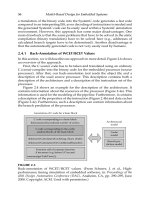
FPGA GPP DSP FPGA
DSRC ASIC FPGA GPP
DSRC DSRC FPGA DSP
ASIC GPP ASIC DSRC
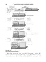
FIGURE 11.1
A heterogenous SoC template.
• A multicore organization can contribute to the energy efficiency of a
SoC. The best energy savings can be obtained by simply switching
off cores that are not used, which also helps in reducing the static
power consumption. Furthermore, the processing of local data in small
autonomous cores abides by the locality of reference principle. More-
over, a core processor can be adaptive; it does not have to run at
full clock speed to achieve the required QoS at a particular moment
in time.
• When one of the cores is discovered to be defect (either because of a
manufacturing fault or discovered at operating time by the built-in
diagnosis), this defective core can be switched off and isolated from
the rest of the design.
• A multicore approach also eases verification of an integrated circuit
design, since the design of identical cores has to be verified only once.
The design of a single core is relatively simple and therefore a lot of
effort can be put in (area/power) optimizations on the physical level
of integrated circuit design.
• The computational power of a multicore architecture scales linearly
with the number of cores. The more cores there are on a chip, the
more computations can be done in parallel (provided that the network
capacity scales with the number of cores and there is sufficient paral-
lelism in the application).
• Although cores operate together in a complex system, an individual
tile operates quite autonomously. In a reconfigurable multicore archi-
tecture, every processing core is configured independently. In fact, a
core is a natural unit of partial reconfiguration. Unused cores can be
configured for a new task, while at the same time other cores continue
performing their tasks. That is to say, a multicore architecture can be
reconfigured partly and dynamically.
Nicolescu/Model-Based Design for Embedded Systems 67842_C011 Finals Page 327 2009-10-2
Reconfigurable MultiCore Architectures 327
11.1.2.1 Heterogeneous Multicore SoC
The reason for heterogeneity in a SoC is efficiency, because typically some
algorithms run more efficiently on bit-level reconfigurable architectures (e.g.,
PN-code generation), some on DSP-like architectures, and some perform
optimal on word-level reconfigurable platforms (e.g., FIR filters or FFT algo-
rithms). We distinguish four processor types: “GPP,” “fine-grained reconfig-
urable” hardware (e.g., FPGA), “coarse-grained” reconfigurable hardware,
and “dedicated” hardware (e.g., ASIC). The different tile processors (TPs) in
the SoC are interconnected by a NoC. Both SoC and NoC are dynamically
reconfigurable, which means that the programs running on the processing
tiles as well as the communication channels are configured at run-time. The
idea of heterogeneous processing elements (PEs) is that one can match the
granularity of the algorithms with the granularity of the hardware. Appli-
cation designers or high-level compilers can choose the most efficient pro-
cessing core for the type of processing needed for a given application task.
Such an approach combines performance, flexibility, and energy efficiency.
It supports high performance through massive parallelism, it matches the
computational model of the algorithm with the granularity and capabilities
of the processing entity, and it can operate at minimum supply voltage and
clock frequency and hence provides energy efficiency and flexibility at the
right granularity only when and where needed and desirable. A thorough
understanding of the algorithm domain is crucial for the design of
an (energy-)efficient reconfigurable architecture. The architecture should
impose little overhead to execute the algorithms in its domain. Streaming
applications form a rather good match with multicore architectures: the com-
putation kernels can be mapped on cores and the streams to the NoC links.
Interprocessor communication is in essence also overhead, as it does not
contribute to the computation of an algorithm. Therefore, there needs to be
a sound balance between computation and interprocessor communication.
These are again motivations for a holistic approach.
11.1.3 Design Criteria for Streaming Applications
In this section, the key design criteria of multicore architectures for streaming
applications are introduced.
11.1.3.1 Predictable and Composable
To manage the complexity of streaming DSP applications, predictable tech-
niques are needed. For example, the NoC as well as the core processors
should provide latency and throughput guarantees. One reason for pre-
dictability is that the amount of data in streaming DSP applications is so
high that even a large buffer would be too small to compensate for unpre-
dictably behaving components and that the latency that these buffers would
introduce is not acceptable in typical streaming DSP applications. A second
reason for using predictable techniques is composability. This means that in
Nicolescu/Model-Based Design for Embedded Systems 67842_C011 Finals Page 328 2009-10-2
328 Model-Based Design for Embedded Systems
case multiple applications are mapped on the same platform, the behavior
of one application should not influence another application. Furthermore,
in streaming applications, there are often hard deadlines at the beginning
of the chain (e.g., sampling rate of an A/D converter) or at the end of the
chain (e.g., fixed rate of the D/A converter, or update rate of the screen).
In other applications such as phased array applications, individual paths of
signals should be exactly timed before they can be combined. Also in these
applications the data rate is so high (e.g., 100 M samples/s) that buffering of
data is not useful. Unfortunately, future semiconductor technologies intro-
duce more uncertainty. Design techniques will have to include resiliency at
the circuit and microarchitecture level to deal with these uncertainties and
the variability at the device technology level. One of the future challenges is
to design predictable systems with unpredictable components.
11.1.3.2 Energy Efficiency
Energy efficiency is an important design issue in streaming DSP applica-
tions. Because portable devices rely on batteries, the functionality of these
devices is strictly limited by the energy consumption. There is an exponen-
tial increase in demand for streaming communication and processing for
wireless protocol baseband processing and multimedia applications, but the
energy content of batteries is increasing at a pace of 10% per year. Also for
high-performance computing there is a need for energy-efficient architec-
tures to reduce the costs for cooling and packaging. In addition to that, there
are also environmental concerns that urge for more efficient architectures in
particular for systems that run 24h per day such as wireless base stations and
search engines (e.g., Google has an estimated server park of 1 million servers
that run 24 h per day).
Today, most components are fabricated using CMOS technology. The
dominant component of energy consumption (85%–90%) in 130 nm CMOS
technology is dynamic power consumption. However, when technology
scales to lower dimensions, the static power consumption will become more
and more pronounced. A first-order approximation of the dynamic power
consumption of CMOS circuitry is given by the formula (see [13]):
P
d
= α · C
eff
·f · V
2
(11.1)
where
P
d
is the power in Watts
C
eff
is the effective switch capacitance in Farads
V is the supply voltage in Volts
α the activity factor
f is the frequency of operations in Hertz
Equation 11.1 suggests that there are basically four ways to reduce power:
reduce the capacitive load C
eff
, reduce the supply voltage V, reduce the
switching frequency f, and/or reduce the activity α. In the context of this
chapter, we will mainly address reducing the capacitance.
Nicolescu/Model-Based Design for Embedded Systems 67842_C011 Finals Page 329 2009-10-2
Reconfigurable MultiCore Architectures 329
As shown in Equation 11.1, energy consumption in CMOS circuitry is
proportional to capacitance. Therefore energy consumption can be reduced
by minimizing the capacitance. This can not only be reached at the
technological level, but much profit can be gained by an architecture that
exploits locality of reference. Connections to external components typically
have much higher capacitance than connections to on-chip resources. There-
fore, to save energy, the designer should use few off-chip wires, and have
them toggle as infrequently as possible. Consequently, it is beneficial to use
on-chip memories such as caches, scratchpads, and registers.
References to memory typically display a high degree of temporal and
spatial locality of reference. Temporal locality of reference refers to the obser-
vation that referenced data is often referenced again in the near future.
Spatial locality of reference refers to the observation that once a particular
location is referenced, a nearby location is often referenced in the near future.
Accessing a small and local memory is much more energy efficient than
accessing a large distant memory. Transporting a signal over a 1 mm wire in
a 45 nm technology requires more than 50 times the energy of a 32-bit oper-
ation in the same technology (the off-chip interconnect consumes more than
a 1000 times the energy of an on-chip 32-bit operation). A multicore architec-
ture intrinsically encourages the usage of small and local on-core memories.
Exploiting the locality of the reference principle extensively improves the
energy efficiency substantially. Because of the locality of reference principle,
the communications within a core are more frequent than between cores.
11.1.3.3 Programmability
Design automation tools form the bridge between processing hardware and
application software. Design tools are the most important requirement for
the viability of multicore platform chips. Such tools reduce the design cycle
(i.e., cost and time-to-market) of new applications. The application program-
mer should be provided with a set of tools that on the one hand hides the
architecture details but on the other hand gives an efficient mapping of the
applications onto the target architecture. High-level language compilers for
(DSP) domain-specific architectures are far more complex than compilers for
general-purpose superscalar architectures because of the data dependency
analysis,instructionscheduling,andallocation.Besidestoolingforapplication
development, tooling for functional verification and debugging is required
for programming multicore architectures. Ingeneral,suchtooling comprises
• General HDL simulation software that provides full insight into the
hardware state, but is extremely slow and not suited for software engi-
neers
• Dedicated simulation software that provides reasonable insight into
the hardware state, performs better than general hardware simulation
software, and can be used by software engineers
• Hardware prototyping boards that achieve great simulation speeds,
but provide poor insight into the hardware state and are not suited
for software engineers
Nicolescu/Model-Based Design for Embedded Systems 67842_C011 Finals Page 330 2009-10-2
330 Model-Based Design for Embedded Systems
By employing the tiled SoC approach, as proposed in Figure 11.1, various
kinds of parallelism can be exploited. Depending on the core architecture one
or more levels of parallellism are supported.
• Thread-level parallelism is explicitly addressed by the multicore
approach as different tiles can run different threads.
• Data-level parallelism is achieved by processing cores that employ par-
allelism in the data path.
• Instruction-level parallelism is addressed by processing cores when mul-
tiple data path instructions can be executed concurrently.
11.1.3.4 Dependability
With every new generation of CMOS technology (i.e., 65 nm and beyond)
the yield and reliability of manufactured chips deteriorate. To effectively
deal with the increased defect density, efficient methods for fault detec-
tion, localization, and fault recovery are needed. Besides yield improvement,
such techniques also improve the long-term reliability and dependability of
silicon-implemented embedded systems. In the ITRS 2003 roadmap (see [1]),
it is indicated that “Potential solutions are adaptive and selfcorrecting, self-
repairing circuits and the use of on-chip reconfigurability.” Modern static
and dynamic fault detection and localization techniques and design-for-test
(DFT) techniques are needed for advanced multicore designs. Yield and reli-
ability can be improved by (dynamically) circumventing the faulty hardware
in deep-submicron chips. The latter requires run-time systems software. This
software detects defective cores and network elements and deactivates these
resources at run-time. The tests are performed while the chip is already in the
field. These self-diagnosis and self-repair hardware and software resources
need to be on chip.
11.2 Classification
Different hardware architectures are available in the embedded systems
domain to perform DSP functions and algorithms: “GPP, DSP, (re-) con-
figurable hardware, and application-specific hardware.” The application-
specific hardware is designed for a dedicated function and is usually referred
to as ASIC. The ASIC is, as its name suggests, an application-specific proces-
sor that has been implemented in an IC.
These hardware architectures have different characteristics in relation to
“performance, flexibility” or “programmability,” and “energy efficiency.”
Figure 11.2 depicts the trade-off in flexibility and performance for differ-
ent hardware architectures. Generally, more flexibility implies a less energy-
efficient solution.
Nicolescu/Model-Based Design for Embedded Systems 67842_C011 Finals Page 331 2009-10-2
Reconfigurable MultiCore Architectures 331
GPP
DSP
Fine-grained
Reconfigurable hardware
Coarse-grained
ASIC
HighFlexibilityLow
Low Performance High
FIGURE 11.2
Flexibility versus performance trade-off for different hardware architectures.
Crucial for the fast and efficient realization of a multiprocessor system-
on-chip (MP-SoC) is the use of predesigned modules, the so-called build-
ing blocks. In this section, we will first classify these building blocks, and
then classify the MP-SoCs that can be designed using these building blocks
together with the interconnection structures between these blocks.
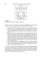
A basic classification of MP-SoC building blocks is given in Figure 11.3.
The basic PEs of an MP-SoC are run-time reconfigurable cores and fixed
cores. The functionality of a run-time reconfigurable core is fixed for a rela-
tively long period in relation to the clock frequency of the cores. Fine-grained
reconfigurable cores are reconfigurable at bit level while coarse-grained
reconfigurable cores are reconfigurable at word level (8 bit, 16 bit, etc.).
Two other essential building blocks are memory and I/O blocks. Designs of
MP-SoCs can be reused to build larger MP-SoCs, increasing the designers
productivity.
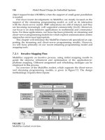
A classification of MP-SoCs is given in Figure 11.4. An MP-SoC basi-
cally consists of multiple building blocks connected by means of an intercon-
nect. If an MP-SoC consists of multiple building blocks of a single type, the
MP-SoC is referred to as “homogeneous.” The homogeneous MP-SoC
architectures can be subdivided into single instruction multiple data
(SIMD), multiple instruction multiple data (MIMD), and array architectures.
Nicolescu/Model-Based Design for Embedded Systems 67842_C011 Finals Page 332 2009-10-2
332 Model-Based Design for Embedded Systems
MP-SoC building blocks
Fixed
cores
Run-time
reconfigurable
cores
Memory
I/O
Fine
grain
Coarse
grain
General
purpose
Design-time
reconfigurable
cores
(ARM)
(SPARC)
(FPGA) (MONTIUM)
(Silicon hive)
(Tensilica)
ASIC
FIGURE 11.3
Classification of MP-SoC building blocks for streaming applications.
MP-SoC architectures
Homogeneous
Heterogeneous
Interconnect
Bus
Network-on-chip
Dedicated
Packet switched Circuit switchedSIMD
MIMD Array
FIGURE 11.4
Classification of MP-SoC architectures and interconnect structures for
streaming applications.
Examples of these architectures will be given below. If multiple types of
building blocks are used, the MP-SoC is called “heterogeneous.”
To interconnect the different building blocks, three basic classes can be
identified: bus, NoC, and dedicated interconnects. A bus is shared between
different processing cores and is a notorious cause of unpredictability.
Unpredictability can be circumvented by an NoC [9]. Two types can be iden-
tified: packet-switched and circuit-switched. Besides the use of these more
or less standardized communication structures, dedicated interconnects are
still widely used. Some examples of different MP-SoC architectures are pre-
sented in Table 11.1.
Nicolescu/Model-Based Design for Embedded Systems 67842_C011 Finals Page 333 2009-10-2
Reconfigurable MultiCore Architectures 333
TABLE 11.1
Examples of Different MP-SoC Architectures
Class Example
SIMD Linedancer (see Section 11.3.2)
Geforce G80 [3]
Xetal [19]
Homogeneous MIMD Tilera (see Section 11.3.4)
Cell [21]
Intel Tflop processor [25]
Array PACT (see Section 11.3.3)
ADDRESS [2]
Heterogeneous A
NNABELLE (see Section 11.3.1)
Silicon Hive [12]
11.3 Sample Architectures
11.3.1 MONTIUM/ANNABELLE System-on-Chip
11.3.1.1 MONTIUM Reconfigurable Processing Core
The M
ONTIUM is an example of a coarse-grained reconfigurable processing
core and targets the 16-bit DSP algorithm domain. The M
ONTIUM architec-
ture origins from research at the University of Twente [18,22]. The M
ONTIUM
processing core has been further developed by Recore Systems [23]. A sin-
gle M
ONTIUM processing tile is depicted in Figure 11.5. At first glance the
M
ONTIUM architecture bears a resemblance to a very large instruction word
(VLIW) processor. However, the control structure of the M
ONTIUM is very
different. The lower part of Figure 11.5 shows the communication and con-
figuration unit (CCU) and the upper part shows the coarse-grained reconfig-
urable M
ONTIUM TP.
11.3.1.1.1 Communication and Configuration Unit
The CCU implements the network interface controller between the NoC and
the M
ONTIUM TP. The definition of the network interface depends on the
NoC technology that is used in a SoC in which the M
ONTIUM processing
tile is integrated [11]. The CCU enables the M
ONTIUM TP to run in “stream-
ing” as well as in “block” mode. In “streaming” mode the CCU and the
M
ONTIUM TP run in parallel. Hence, communication and computation over-
lap in time. In “block” mode, the CCU first reads a block of data, then starts
the M
ONTIUM TP, and finally after completion of the MONTIUM TP, the CCU
sends the results to the next processing unit in the SoC (e.g., another M
ONTIUM
Nicolescu/Model-Based Design for Embedded Systems 67842_C011 Finals Page 334 2009-10-2
334 Model-Based Design for Embedded Systems
PPA
M01 M02
ALU1
ABCD
Out2 Out1
E
M03 M04
ALU2
ABCD
Out2 Out1
WE
M05 M06
ALU3
ABCD
Out2 Out1
WE
M07 M08
ALU4
ABCD
WE
M09 M10
ALU5
ABCD
W
Memory
decoder
Inter-
connect
decoder
Register
decoder
ALU
decoder
Sequencer
Communication and configuration unit
Out2 Out1 Out1Out2
FIGURE 11.5
The M
ONTIUM coarse-grained reconfigurable processing tile.
processing tile or external memory). Hence, communication and computa-
tion are sequenced in time.
11.3.1.1.2 M
ONTIUM Tile Processor
The TP is the computing part of the M
ONTIUM processing tile. The MONTIUM TP
can be configured to implement a particular DSP algorithm. DSP algorithms
that have been implemented on the M
ONTIUM are, for instance, all power of 2
FFTs upto 2048 points, non-power of 2 FFT upto FFT 1920, FIR filters, IIR
filters, matrix vector multiplication, DCT decoding, Viterbi decoders, and
Turbo (SISO) decoders. Figure 11.5 reveals that the hardware organization
of the M
ONTIUM TP is very regular. The five identical arithmetic logic units
(ALU1 through ALU5) in a tile can exploit data level parallellism to enhance
performance. This type of parallelism demands a very high memory band-
width, which is obtained by having 10 local memories (M01 through M10) in
parallel. The small local memories are also motivated by the locality of ref-
erence principle. The data path has a width of 16 bit and the ALUs support
both signed integer and signed fixed-point arithmetic. The ALU input regis-
ters provide an even more local level of storage. Locality of reference is one of
the guiding principles applied to obtain energy efficiency in the M
ONTIUM TP.
Nicolescu/Model-Based Design for Embedded Systems 67842_C011 Finals Page 335 2009-10-2
Reconfigurable MultiCore Architectures 335
A vertical segment that contains one ALU together with its associated input
register files, a part of the interconnect, and two local memories is called
a processing part (PP). The five PPs together are called the processing part
array (PPA).
A relatively simple sequencer controls the entire PPA. The sequencer
selects configurable PPA instructions that are stored in the decoder blocks
of Figure 11.5. For (energy) efficiency it is imperative to minimize the con-
trol overhead. The PPA instructions, which comprise ALU, AGU, memory,
register file, and interconnect instructions, are determined by a DSP appli-
cation designer at design time. All M
ONTIUM TP instructions are scheduled
at design time and arranged into a M
ONTIUM sequencer programme. By stat-
ically scheduling the instructions as much as possible at compile time, the
M
ONTIUM sequencer does not require any sophisticated control logic which
minimizes the control overhead of the reconfigurable architecture.
The M
ONTIUM TP has no fixed instruction set, but the instructions are con-
figured at configuration time. During configuration of the M
ONTIUM TP, the
CCU writes the configuration data (i.e., instructions of the ALUs, memories
and interconnects, etc., sequencer and decoder instructions) in the configu-
ration memory of the M
ONTIUM TP. The size of the total configuration mem-
ory of the M
ONTIUM TP is about 2.6 kB. However, configuration sizes of DSP
algorithms mapped on the M
ONTIUM TP are typically in the order of 1 kB.
For example, a 64-point fast Fourier transform (FFT) has a configuration
size of 946 bytes. By sending a configuration file containing configuration
RAM addresses and data values to the CCU, the M
ONTIUM TP can be con-
figured via the NoC interface. The configuration memory of the M
ONTIUM
TP is implemented as a 16-bit wide SRAM memory that can be written by
the CCU. By only updating certain configuration locations of the configu-
ration memory, the M
ONTIUM TP can be partially reconfigured. In the con-
sidered M
ONTIUM TP implementation, each local SRAM is 16-bit wide and
has a depth of 1024 addresses, which results in a storage capacity of 2kB
per local memory. The total data memory inside the M
ONTIUM TP adds up
to a size of 20 kB. A reconfigurable address generation unit (AGU) is inte-
grated into each local memory in the PPA of the M
ONTIUM TP. It is also
possible to use the local memory as a look-up table (LUT) for complicated
functions that cannot be calculated using an ALU, such as sine or division
(with one constant). The memory can be used in both integer or fixed-point
LUT mode.
11.3.1.2 Design Methodology
Development tools are essential for quick implementation of applications in
reconfigurable architectures. The M
ONTIUM development tools start with a
high-level description of an application (in C/C++ or M
ATLAB
R
)andtrans-
late this description to a M
ONTIUM TP configuration [16]. Applications can
be implemented on the M
ONTIUM TP using an embedded C language, called