Optical Networks: A Practical Perspective - Part 26 ppsx
Bạn đang xem bản rút gọn của tài liệu. Xem và tải ngay bản đầy đủ của tài liệu tại đây (711.25 KB, 10 trang )
220 COMVONrNTS
3.8.3
The advantage of CGM is that it is conceptually simple. However, there are
several drawbacks. The achievable extinction ratio is small (less than 10) since the
gain does not really drop to zero when there is an input 1 bit. The input signal power
must be high (around 0 dBm) so that the amplifier is saturated enough to produce a
good variation in gain. This high-powered signal must be eliminated at the amplifier
output by suitable filtering, unless the signal and probe are counterpropagating.
Moreover, as the carrier density within the SOA varies, it changes the refractive
index as well, which in turn affects the phase of the probe and creates a large
amount of pulse distortion.
Interferometric Techniques
The same phase-change effect that creates pulse distortion in CGM can be used
to effect wavelength conversion. As the carrier density in the amplifier varies with
the input signal, it produces a change in the refractive index, which in turn mod-
ulates the phase of the probe~hence we use the term
cross-phase
modulation for
this approach. This phase modulation can be converted into intensity modulation
by using an interferometer such as a Mach-Zehnder interferometer (MZI) (see Sec-
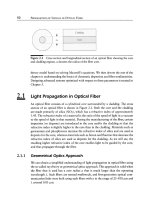
tion 3.3.7). Figure 3.78 shows one possible configuration of a wavelength converter
using cross-phase modulation. Both arms of the MZI have exactly the same length,
with each arm incorporating an SOA. The signal is sent in at one end (A) and the
probe at the other end (B). If no signal is present, then the probe signal comes
out unmodulated. The couplers in the MZI are designed with an asymmetric cou-
pling ratio ?' -r 0.5. When the signal is present, it induces a phase change in each
amplifier. The phase change induced by each amplifier on the probe is different be-
cause different amounts of signal power are present in the two amplifiers. The MZI
translates this relative phase difference between its two arms on the probe into an
intensity-modulated signal at the output.
This approach has a few interesting properties. The natural state of the MZI
(when no input signal is present) can be arranged to produce either destructive or
constructive interference on the probe signal. Therefore we can have a choice of
whether the data coming out is the same as the input data or is complementary.
The advantage of this approach over CGM is that much less signal power is
required to achieve a large phase shift compared to a large gain shift. In fact, a
low signal power and a high probe power can be used, making this method more
attractive than CGM. This method also produces a better extinction ratio because the
phase change can be converted into a "digital" amplitude-modulated output signal
by the interferometer. So this device provides regeneration with reshaping (2R) of
3.8 Wavelength Converters 221
Figure
3.78 Wavelength conversion by cross-phase modulation using semiconductor optical am-
plifiers embedded inside a Mach-Zehnder interferometer.
the pulses. Depending on where the MZI is operated, the probe can be modulated
with the same polarity as the input signal, or the opposite polarity. Referring to
Figure 3.78, where we plot the power coupled out at the probe wavelength versus
the power at the signal wavelength, depending on the slope of the demultiplexer, a
signal power increase can either decrease or increase the power coupled out at the
probe wavelength. Like CGM, the bit rate that can be handled is at most 10 Gb/s
and is limited by the carrier lifetime. This approach, however, requires very tight
control of the bias current of the SOA, as small changes in the bias current produce
refractive index changes that significantly affect the phase of signals passing through
the device.
We have seen above that the CPM interferometric approach provides regenera-
tion with reshaping (2R) of the pulses. As we saw earlier, while 2R cleans up the
signal shape, it does not eliminate phase (or equivalently timing) jitter in the signal,
which would accumulate with each such 2R stage. In order to completely clean up
the signal, including its temporal characteristics, we need regeneration with reshap-
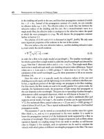
ing and retiming (3R). Figure 3.79 shows one proposal for accomplishing this in
222
COMPONENTS
Figure 3.79 All-optical regeneration with reshaping and retiming (3R) using a combination of
cross-gain modulation and cross-phase modulation in semiconductor optical amplifiers. (After
[Chi97].)
3.8 Wavelength Converters 223
3.8.4
the optical domain without resorting to electronic conversion [Chi97, Gui98]. The
approach uses a combination of CGM and CPM. We assume that a local clock is
available to sample the incoming data. This clock needs to be recovered from the
data; we will study ways of doing this in Section 12.2. The regenerator consists of
three stages. The first stage samples the signal. It makes use of CGM in an SOA.
The incoming signal is probed using two separate signals at different wavelengths.
The two probe signals are synchronized and modulated at twice the data rate of
the incoming signal. Since the clock is available, the phase of the probe signals is
adjusted to sample the input signal in the middle of the bit interval. At the output of
the first stage, the two probe signals have reduced power levels when the input signal
is present and higher power levels when the input signal is absent. In the second
stage, one of the probe signals is delayed by half a bit period with respect to the
other. At the output of this stage, the combined signal has a bit rate that matches the
bit rate of the input signal and has been regenerated and retimed. This signal is then
sent through a CPM-based interferometric converter stage, which then regenerates
and reshapes the signal to create an output signal that has been regenerated, retimed,
and reshaped.
Wave Mixing
The four-wave mixing phenomenon that occurs because of nonlinearities in the trans-
mission medium (discussed in Section 2.4.8) can also be utilized to realize wavelength
conversion. Recall that four-wave mixing causes three waves at frequencies fl, f2,
and f3 to produce a fourth wave at the frequency fl + f2 - f3; when fl = f2, we
get a wave at the frequency
2fl - f3.
What is interesting about four-wave mixing
is that the resulting waves can lie in the same band as the interacting waves. As we
have seen in Section 2.4.8, in optical fibers, the generated four-wave mixing power
is quite small but can lead to crosstalk if present (see Section 5.8.4).
For the purposes of wavelength conversion, the four-wave mixing power can be
enhanced by using an SOA because of the higher intensities within the device. If we
have a signal at frequency fs and a probe at frequency
fp,
then four-wave mixing will
produce signals at frequencies
2fp - fs
and
2fs - fp,
as long as all these frequencies
lie within the amplifier bandwidth (Figure 3.80).
The main advantage of four-wave mixing is that it is truly transparent because
the effect does not depend on the modulation format (since both amplitude and
phase are preserved during the mixing process) and the bit rate. The disadvantages
are that the other waves must be filtered out at the SOA output, and the conversion
efficiency goes down significantly as the wavelength separation between the signal
224
COMPONENTS
Figure 3.80
amplifier.
Wavelength conversion by four-wave mixing in a semiconductor optical
and probe is increased. We will study the conversion efficiency of four-wave mixing
in Section 5.8.4.
Summary
We have studied many different optical components in this chapter. Couplers, isola-
tors, and circulators are all commodity components. Many of the optical filters that
we studied are now commercially available, with fiber gratings, thin-film multicavity
filters, and arrayed waveguide gratings all competing for use in commercial WDM
systems.
Erbium-doped fiber amplifiers (EDFAs) are widely deployed and indeed served
as a key enabler for WDM. EDFA designs today incorporate multiple stages and
gain-flattening filters and provide midstage access between the multiple stages to
insert other elements such as dispersion compensating modules and wavelength
add/drop multiplexers. A new generation of EDFAs providing amplification in the
L-band has recently emerged. We are also now seeing distributed Raman amplifiers
used in conjunction with EDFAs in ultra-long-haul systems.
Semiconductor DFB lasers are used in most high-speed communication systems
today although other single-longitudinal mode laser structures may eventually be-
come viable commercially. Compact semicondunctor tunable lasers are now emerg-
ing as viable commercial devices. High-speed APDs and pinFET receivers are both
available today.
Large-scale MEMS-based optical switches for use in wavelength crossconnects
are now emerging as commercial devices, and a variety of technologies are avail-
able to build smaller-scale switches. All-optical wavelength converters are still in the
research laboratories, awaiting significant cost reductions and performance improve-
ments before they can become practical.
Further Reading 225
Further Reading
The book by Green [Gre93] treats many of the optical components considered in
this chapter in more detail, particularly tunable filters and lasers. See also [KK97]
for more advanced coverage of a number of components.
Most of the filters we described are now commercially available. Gratings are
described in detail in several textbooks on optics, for example, [KF86, BW99]. The
Stimax grating is described in [LL84] and [Gre93]. See [CK94, Ben96, Kas99] for
details on fiber grating fabrication and properties, and [Ven96b, Ven96a] for applica-
tions of long-period gratings. For a description of how dielectric thin-film multicavity
filters work, see [SS96] and [Kni76]. The electromagnetics background necessary to
understand their operation is provided, for example, by [RWv93]. Early papers on
the arrayed waveguide grating are [DEK91] and [VS91]. The principle behind their
operation is described in [McG98, TSN94, TOTI95, TOT96]. The integrated-optics
AOTF is described in [SBJC90, KSHS01], and its systems applications are discussed
in [Che90].
There is an extensive literature on optical amplifiers. See [BOS99, Des94] for
EDFAs, [Flo00] for a summary of L-band EDFAs, and [O'M88] for a tutorial
on SOAs. [Tie95, SMB00, FDW01] provide samples of some recent work on
gain-clamped SOAs. See [NE01, NE00] and [KK97, Chapter 7] for an overview
of Raman amplifiers.
There are several textbooks on the subject of lasers alone; see, for example,
[AD93]. Laser oscillation and photodetection are covered in detail in [Yar97].
[JQE91] is a good reference for several laser-related topics. Other good tutorials
on lasers appear in [BKLW00, LZ89, Lee91, SIA92]. A very readable and up-to-date
survey of vertical cavity lasers can be found in [Har00]. See also [MZB97]. Most
semiconductor lasers today make use of quantum well structures. See [AY86] for
a good introduction to this subject. The mathematical theory behind mode locking
is explained in [Yar89] and [Yar65]. There is an extensive discussion of various
mode-locking methods for fiber lasers in [Agr95]. Lithium niobate external modula-
tors are well described in [Woo00] and [KK97, Chapter 9], and electro-absorption
modulators in [BKLW00] and [KK97, Chapter 4].
There is currently significant effort toward realizing commercially viable tunable
lasers. We refer the reader to [Col00, Har00, AB98, Gre93, KK97] for more in-depth
explorations of this subject. An early review of tunable laser approaches appeared
in [KM88]. The VCSEL-based tunable laser is described in [Vak99]. Other types
of tunable VCSELs have been demonstrated; see, for instance, [CH00, Har00]. The
sampled grating laser structure is explained in [JCC93] and superstructure grating
lasers in [Toh93]. See [WMB92, Rig95] for details on the GCSR laser. The arrayed
external grating-based laser approaches were proposed in [Soo92, ZJ94, Zir96].
Input
226
COMPONENTS
Figure 3.81 A 3 dB coupler with the two outputs connected by a piece of fiber.
The tutorial article by Spanke [Spa87] is a good review of large switch architec-
tures for optical switches. See also [MS88] for a good collection of papers on optical
switching and [Clo53] for the original paper on the Clos switch architecture. The
classic book by Bene~ [Ben65] is the authoritative reference for the mathematical
theory of large switch architectures developed for telephony applications.
A very accessible survey of mechanical switches can be found in [Kas95,
Chapter 13]. Several papers [NR01, LGT98, Nei00, Ryf01, Lao99] describe
MEMS-based switches. The inkjet-based waveguide switch is described in [Fou00].
See [WL96, PS95] for some early papers on liquid crystal switches.
Surveys and comparisons of different types of wavelength converters appear in
[Stu00, EM00, NKM98, Yoo96, ISSV96, DMJ+96, Chi97].
3.1
3.2
Problems
Consider the 3 dB 2 x 2 coupler shown in Figure 3.81. Suppose we connect the two
outputs with a piece of fiber. Assume that the polarizations are preserved through
the device. A light signal is sent in on the first input. What happens? Derive the field
transfer function for the device. Assume the coupler used is a reciprocal device so
that it works exactly the same way if its inputs and outputs are reversed.
Hint:
This
device is called a loop mirror.
Consider a device with three ports where it is desired to send all the energy input
at ports 1 and 2 to port 3. We assume, for generality, that all ports can be used as
inputs and outputs. The scattering matrix of such a device can be written as
0 0 s13 )
S - 0 0 $23 9
$31 $32 $33
Problems 227
3.3
3.4
3.5
3.6
3.7
3.8
3.9
3.10
3.11
Show that a scattering matrix of this form cannot satisfy the conservation of energy
condition, (3.4). Thus it is impossible to build a device that combines all the power
from two input ports to a third port, without loss.
Consider an isolator that is a two-port device where power must be transferred from
port 1 to port 2, but no power must be transferred from port 2 to port 1. The
scattering matrix of such a device can be written as
S_ (Sll s12)
0 $22 "
Show that a scattering matrix of this form cannot satisfy the conservation of energy
condition, (3.4). Thus the loss occurs in the isolator because the power input at port
2 must be absorbed by it. However, the power input at port 1 can be transferred to
port 2 without loss.
In Figure 3.10, show that the path length difference between the rays diffracted at
angle 0a and traversing through adjacent slits is approximately
a[sin(Oi) -
sin(0d)]
when the grating pitch a is small compared to the distance of the source and the
imaging plane from the grating plane.
Derive the grating equation for a blazed reflection grating with blaze angle ~, such
as the one shown in Figure 3.11.
Derive the amplitude distribution of the diffraction pattern of a grating with N
narrow slits spaced distance d apart. Show that we obtain diffraction maxima when
d sin 0 - m)~. Discuss what happens in the limit as N ~ oo.
Show that the resonant frequencies f~ of a Fabry-Perot cavity satisfy
f~ - fo + nAf,
n integer, for some fixed f0 and Af. Thus these frequencies are spaced equally apart.
Note that the corresponding wavelengths are
not
spaced equally apart.
Derive the power transfer function of the Fabry-Perot filter.
Derive the expression (3.13) for the finesse of the Fabry-Perot filter. Assume that the
mirror reflectivity, R, is close to unity.
Show that the fraction of the input power that is transmitted through the Fabry-Perot
filter, over all frequencies, is (1 - R)/(1 + R). Note that this fraction is small for high
values of R. Thus, when all frequencies are considered, only a small fraction of the
input power is transmitted through a cavity with highly reflective facets.
Consider a cascade of two Fabry-Perot filters with cavity lengths 11 and 12, respec-
tively. Assume the mirror reflectivities of both filters equal R, and the refractive index
of their cavities is n. Neglect reflections from the second cavity to the first and vice
228
' COMPONENTS
3.12
3.13
3.14
3.15
3.16
3.17
versa. What is the power transfer function of the cascade? If
11/12 k/m,
where k
and m are relatively prime integers, find an expression for the FSR of the cascade.
Express this FSR in terms of the FSRs of the individual filters.
Show that the transfer function of the dielectric slab filter shown in Figure G.l(b) is
identical to that of a Fabry-Perot filter with facet reflectivity
~/~- n2 -nl
n2+nl
assuming n3 = n
1.
Consider a stack of 2k alternating low-index (nL) and high-index (n/4) dielectric
films. Let each of these films have a quarter-wave thickness at )~0. In the notation of
Section 3.3.6, this stack can be denoted by
(HL) ~.
Find the reflectivity of this stack as
a function of the optical wavelength )~. Thus a single-cavity dielectric thin-film filter
can be viewed as a Fabry-Perot filter with wavelength-dependent mirror reflectivities.
Derive the power transfer function of the Mach-Zehnder interferometer, assuming
only one of its two inputs is active.
Consider the Mach-Zehnder interferometer of Section 3.3.7.
(a) With the help of a block diagram, show how a 1 x n demultiplexer can be
constructed using n - 1 MZIs. Assume n is a power of two. You must specify
the path length differences AL that must be used in each of the MZIs.
(b) Can you simplify your construction if only a specific one of the signals needs
to be separated from the rest of the n - 1 ?
Consider the Rowland circle construction shown in Figure 3.26. Show that the
differences in path lengths between a fixed-input waveguide and any two successive
arrayed waveguides is a constant. Assume that the length of the arc on which the
arrayed waveguides are located is much smaller than the diameter of the Rowland
circle.
Hint:
Choose a Cartesian coordinate system whose origin is the point of
tangency of the Rowland and grating circles. Now express the Euclidean distance
between an arbitrary input (output) waveguide and an arbitrary arrayed waveguide in
this coordinate system. Use the assumption stated earlier to simplify your expression.
Finally, note that the vertical spacing between the arrayed waveguides is constant.
In the notation of the book, this shows that
8i
d
sinOi, where d is the vertical
separation between successive arrayed waveguides, and
Oi
is the angular separation
of input waveguide i from the central input waveguide, as measured from the origin.
Derive an expression for the FSR of an AWG for a fixed-input waveguide i and a
fixed-output waveguide j. The FSR depends on the input and output waveguides.
But show that if the arc length of the Rowland circle on which the input and output
Problems 229
3.18
3.19
3.20
3.21
3.22
3.23
waveguides are located (see Figure 3.26) is small, then the FSR is approximately
constant. Use the result from Problem 3.16 that ~i = d sin 0i.
Consider an AWG that satisfies the condition given in Problem 3.17 for its FSR to
be approximately independent of the input and output waveguides. Given the FSR,
determine the set of wavelengths that must be selected in order for the AWG to
function as the wavelength router depicted in Figure 3.25. Assume that the angular
spacing between the input (and output) waveguides is constant. Use the result from
Problem 3.16 that
c~ i =
d sin
Oi.
Design an AWG that can multiplex/demultiplex 16 WDM signals spaced 100 GHz
apart in the
1.55
#m band. Your design must specify, among other things, the spacing
between the input/output waveguides, the path length difference between successive
arrayed waveguides, the radius R of the grating circle, and the FSR of the AWG.
Assume the refractive index of the input/output waveguides and the arrayed wave-
guides is 1.5. Note that the design may not be unique, and you may have to make
reasonable choices for some of the parameters, which will in turn determine the rest
of the parameters.
Show that the FWHM bandwidth of the acousto-optic filter is ~
0.8)~2/1An.
Explain how the polarization-independent acousto-optic tunable filter illustrated in
Figure 3.28 acts as a two-input, two-output wavelength router when both its inputs
are active.
Calculate the acousto-optic interaction length that would be required for the AOTF
to have a passband width (FWHM) of 1 nm at an operating wavelength of
1.55 #m.
Assume An = 0.07.
Consider a 16-channel WDM system where the interchannel spacing is nominally
100 GHz. Assume that one of the channels is to be selected by a filter with a 1 dB
bandwidth of 2 GHz. We consider three different filter structures for this purpose.
Fabry-Perot filter: Assume the center wavelengths of the channels do not
drift. What is the required finesse and the corresponding mirror reflectivity
of a Fabry-Perot filter that achieves a crosstalk suppression of 30 dB from
each adjacent channel? If the center wavelengths of the channels can drift
up to 4-20 GHz from their nominal values, what is the required finesse and
mirror reflectivity?
[] Mach-Zehnder interferometer: Assume a cascade of MZIs, as shown in Fig-
ure 3.21(c), is used for this purpose and the same level of crosstalk suppres-
sion must be achieved. What is the path length difference AL and the number
of stages required, when the channel center wavelengths are fixed and when
they can drift by +20 GHz?