Advances in Optical and Photonic Devices 2011 Part 11 pptx
Bạn đang xem bản rút gọn của tài liệu. Xem và tải ngay bản đầy đủ của tài liệu tại đây (2.04 MB, 25 trang )
Quantum Dot Photonic Devices and Their Material Fabrications
239
1042.71 nm–ch.4: 1043.85 nm). Each of the central wavelengths is selected for the 100-GHz
channel spacing of the AWG by using the discrete single-mode selection method of the QD-
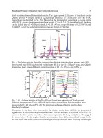
CML. Figure 9(b) shows a typical eye diagram at ch. 2 after transmission. A clear eye
opening at 12.5 Gbps is observed after the transmission. Therefore, the 1-μm waveband with
a 12.5-Gbps transmission over a long-distance (1.5 km) single-mode HF is successfully
YDFA
LN Modulator
1-µm-waveband
single-mode holey-fiber
Distance: 1.48 km
1-µm waveband
Quantum dot
comb-laser (QD-CML)
with mode-selection
YDFA
PPG
1-µm waveband
arrayed waveguide grating
YDFA
0.6-nm
OSA
0.6-nm
Communications
analyzer
12.5-Gbps
0 dBm
Fig. 8. Experimental set-up for testing the 1-μm WDM photonic transport system. A 1-μm
waveband and single-mode selected quantum dot optical-frequency comb laser (QD-CML)
was used for the light source.
1041 1042 1043 1044 1045
-70
-60
-50
-40
-30
-20
-10
0
10
* Arrayed-Waveguide Grating (AWG)
for 1-micron waveband, 100 GHz spacing
* Injection seeded Sb-based QD FP-LD
Ch4Ch3Ch2Ch1
Recieved power (dBm)
Wavelength (nm)
After 1.5 km transmission
20 ps/div
1043.2 nm (Ch2)
After 1.5 km transmission
20 ps/div
1043.2 nm (Ch2)
(b)
(a)
Fig. 9. (a) Optical spectrum of 12.5-Gbps and single-mode selected QD-CML after 1.5-km
transmission of the holey fiber. (b) Eye opening of ch.2 after transmission.
Advances in Optical and Photonic Devices
240
achieved at four different wavelengths by using a wavelength-tunable discrete single-mode
selected QD laser device. The 1-μm waveband AWG, YDFAs, and other passive devices are
also important to construct the 1-μm waveband photonic transport system. From these
results, a 12.5-Gbps-based WDM photonic transmission with a 100-GHz channel spacing can
be realized in the 1-μm waveband by using the proposed methods. Additionally, it is
expected that the QD photonic devices such as a semiconductor laser fabricated on the GaAs
wafer will become a powerful candidate to realize an ultra-broadband 1- to 1.3-μm photonic
transport system.
3. Quantum dot structure for advanced photonic devices
In this section, novel material systems of a QD structure are introduced for advanced
photonic devices. The novel materials of the QD are expected to be used in laser device
fabrication, silicon photonics, visible light-emitting devices, etc.
3.1 Long-wavelength quantum dot structure
Sb-based III-V semiconductor materials have very narrow-band gap properties. Therefore,
the use of Sb-based III-V semiconductor QD structures (the Sb atoms are included in the QD
structure) are expected for producing long-wavelength-emitting devices (Yamamoto et al.
2005 & 2006b). In this section, the Sb-based QD structure fabricated on a GaAs substrate is
introduced. However, the fabrication of the Sb-based QD such as an InGaSb QD is difficult
under conventional QD growth conditions with the MBE method. To form the high-quality
Sb-based QD structure, a Si atom irradiation technique is proposed as one of the methods
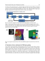
for surface treatment. Figure 10(a) shows a schematic image of the Si atom irradiation
GaAs
GaAs
GaAs
GaAs
Reducing surface free energy :σ
s
Enhanced S-K growth mode:σ
s
<σ
f
(σ
f
: Film free-energy)
High-density Sb-based QD structure
Silicon atom irradiation technique
Silicon
In, Ga and Sb
InGaSb QD
(a)
(b)
(c)
Fig. 10. (a) Schematic image of silicon atom irradiation technique for the fabrication of the
high-quality QD structure. AFM images of InGaSb QD structure in a 5 × 5 -μm
2
region on
GaAs substrate without (b) and with (c) the Si atom irradiation technique.
Quantum Dot Photonic Devices and Their Material Fabrications
241
technique. Low density Si atoms are irradiated on to the GaAs surface immediately before
the Sb-based QD structure growth. It is expected that the surface free-energy may be
reduced with the irradiation of Si atoms. Therefore, the density of the Sb-based QD structure
is enhanced by using this atom-irradiation technique. Figures 10(b) and (c) show the AFM
images of the Sb-based QD structure without and with the Si atom irradiation, respectively.
It is found that the QD density with Si atoms is approximately 100 times higher than that
without Si atoms. Generally, the QD density as high as 10
10
/cm
2
is necessary if the QD
structure is used for developing a laser or other photonic devices. Therefore, the
optimization of the QD growth conditions such as growth-rate, As-flux intensity, and
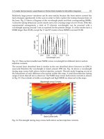
temperature is also important to obtain the high-quality QD structure. Figure 11(a) shows an
AFM image of the Sb-based QD/GaAs structure under the optimized growth conditions.
The height, dimension, and density of the Sb-based QD are approximately 7.5 nm, 25 nm,
and 2 × 10
10
/cm
2
, respectively.
An ultra-wideband emission between wavelengths of 1.08- and 1.48-μm can be successfully
realized by using the Sb-based QD/GaAs structure, as shown in Fig. 11(b). The long-
wavelength and ultra-broadband emission is also obtained from a light-emitting diode
(LED) that contained the Sb-based QD in active regions. From this result, it is expected that
ultra-broadband wavelength (>350 nm) light sources may be achieved with the QD
structure for the O-, E-, S-, and C-band (Yamamoto et al. 2009a).
1000 1200 1400 1600
Emission (dB)
Ultra-wideband
InGaSb QDs
with Si atom irradiation technique
at Room temperature
Wavelength (nm)
(b)(a)
Fig. 11. (a) Atomic force microscope image of high-quality Sb-based QD (InGaSb QD)
structure on GaAs surface. (b) Ultra broadband and long-wavelength emission from the Sb-
based QD/GaAs structure.
The combination of a micro-cavity structure and the QD structure is a very interesting
device structure for the investigation of cavity quantum-electrodynamics (QED). Study on
the QED of the QD structure is important for constructing a quantum communications
system (Ishi-Hayase et al. 2007 & Kujiraoka et al. 2009). A vertical cavity structure and a
photonic crystal structure as an optical resonator are useful for confining the photons
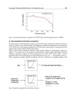
(Nomura et al. 2009). Figure 12(a) presents a cross-sectional image of a fabricated vertical
Advances in Optical and Photonic Devices
242
cavity structure, which include the Sb-based QD in the cavity. A high-performance
diffractive Bragg reflector (DBR) for accomplishing the vertical cavity structure can be
simply produced by using an AlGaAs material system. From the Sb-based QD structure in
the vertical cavity, a 1.55-μm sharp emission peak, as shown in Fig. 12(b), is successfully
observed under the optically pumped condition (Yamamoto et al. 2006a). It is also found
that a long-wavelength emission with a 1.52-μm peak can be obtained from the similar QD
in the cavity structure at room temperature with a current injection. Therefore, it is expected
that the use of the long wavelength QD active media in the semiconductor micro-cavity
structure is a very useful and important way for fabricating long-wavelength and
multiwavelength vertical cavity surface emitting lasers (VCSELs), resonant cavity light-
emitting diodes (RCLEDs), single photon sources, etc.
n- doped
GaAs/AlGaAs
DBR mirrors
p- doped
GaAs/AlGaAs
DBR mirrors
Cross-sectional
image of vertical
cavity structure
Stacked InGaSb
QDs active layer
Sb-based Quantum Dot
(a) (b)
Fig. 12. (a) Sb-based QD in micro cavity structure and (b) 1.55-μm wavelength emission
spectrum from optically pumped vertical cavity structure.
3.2 Quantum dot and related materials for silicon photonics
Silicon photonics technology has been conventionally used to fabricate high performance
photonic circuits, which have low-power-consumption, are compact, and are relatively
inexpensive to fabricate (Liu et al. 2004 & Yamamoto et al. 2007b). Poly-, amorphous-, and
crystalline-Si waveguide devices have been developed and their properties have been
investigated. An optical gain region must be provided for silicon waveguide structures to
enable the fabrication of active devices such as light emitters and optical amplifiers on
silicon platforms (Balakrishnan et al. 2006). As one of the candidates of the optical gain
media, a III-V semiconductor QD structure on a Si wafer has been investigated. Figure 13
shows the schematic image of the Sb-based QD/Si structure and AFM images of the Sb-
based QD structures grown between 400°C and 450°C on Si substrates (Yamamoto et al.
2007a). From the AFM image, it is found that the high-quality and high-density Sb-based
QD structure can be obtained under the optimal growth conditions by MBE. Therefore, a
Quantum Dot Photonic Devices and Their Material Fabrications
243
high-density (>10
10
/cm
2
) and small-sized (<10 nm) QD structure can be obtained by
growing the QDs below 400°C. From this result, it is expected that the nanostructured Sb-
based semiconductors with a low-temperature process (<400°C) should become useful
materials for complementary metal oxide semiconductor (CMOS) devices compatible with
silicon photonics technology (Yamamoto et al. 2008a). Additionally, it is also expected that
the nanostructured Sb-based semiconductor will be used for high-speed electro-devices,
because the III-Sb compound semiconductor has high-mobility characteristics (Ashley et al.,
2007).
Silicon (001)
InGaSb QD
(b) (c)
(a)
Fig. 13. (a) Schematic image of Sb-based QD structure on Si wafer, and AFM images of the
Sb-based QD on Si at (b) 400°C and (c) 450°C.
Compound semiconductors are widely studied for the fabrication of the QD structure
because they exhibit an observable quantum size effect in the quantum confinement
structure of a relatively large size (approximately few tens of nanometers). On the other
hand, a carrier confined structure several nanometers in size, which is generally called a
nanoparticle, is necessary when using a silicon semiconductor material. Several techniques
have been proposed for the fabrication of the Si nanoparticle as a Si-QD structure (Canham
et al. 1990). An anodization method and a photochemical etching method of a Si wafer are
proposed for producing the Si nanoparticles (Yamamoto et al. 2001 & Hadjersi et al. 2004). It
is known that the Si nanoparticle exhibits a bright visible light emission of red or blue color,
and it is considered that this light emission is caused by the quantum size effect of the Si-
QD. Figure 14(a) shows a visible emission spectrum from the photochemically etched layers,
such as Si nanoparticles (Yamamoto et al. 1999). In addition, electroluminescence devices on
a Si wafer are also demonstrated using Si nanoparticles, as shown in Figure 14(b). It is
expected that the Si nanoparticle as the Si-QD structure will become a useful material for the
visible light-emitting devices with Si-based electric devices (Yamamoto et al. 2000).
4. Conclusion
The quantum dot (QD) structures are intensively investigated as the three-dimensional
carrier confined structure. It is expected that the QD structure can act likely as an atom,
which has a controllable characteristic of energy levels. The semiconductor QD structure is a
very important material for developing novel photonic devices. In this chapter, fabrication
techniques and characteristics of novel QD photonic devices such as a broadband QD light
Advances in Optical and Photonic Devices
244
500600700800
Area-B
Area-A
Area-BArea-A
Si wafer
Selective area formation of
Photo-chemically etched silicon
Normalized PL intensity
Wavelength(nm)
Visible electroluminescence
Light emitting device
by using photo-chemically etched Si
Fig. 14. (a) Emission spectra of photochemically etched layers as Si nanoparticles. The
emission colors in areas A and B are observed as yellow and red, respectively. Each layer is
formed on the same Si substrate using a selective area formation technique. (b) Visible
electroluminescence devices on Si wafer by using the Si-particle as the Si-QD.
source and a wavelength tunable QD laser were explained. The QD light source act in a
broad wavelength band between 1-μm and 1.3-μm can be fabricated on the GaAs substrate
as a low cost and large-sized wafer by using InAs QD and InGaAs QD structures as an
active media. In addition, a fabrication technique of the Sb-based QD structures on the GaAs
substrate was demonstrated for the ultra-broadband light source between 1 and 1.55 μm,
and the novel photonic devices using the cavity-QED. In other words, by using the QD
structure, ultra-broadband optical gain media can be achieved for broadband light-emitting
diodes, wavelength tunable laser diodes, semiconductor optical amplifiers, etc.
Additionally, the QD structures have interesting opto-electric characteristics compared to
the conventional quantum well and bulk materials. It is expected that the QD optical
frequency comb laser (QD-CML) can be realized by using the useful characteristics of the
QD structure.
Ultra-broadband optical frequency resources in the short wavelength band such as the 1-μm
waveband can be used for optical communications. As the 1-μm waveband photonic
transport system, over 10 Gbps and a long distance transmission were successfully
demonstrated by using high-performance key components such as single-mode QD light
sources, long-distance holey fibers, and YDFAs. Therefore, it is expected that the uses of the
QD photonic devices enhance the usable waveband for optical communications.
For the silicon photonics, a fabrication technique for the high-quality Sb-based QD structure
on a Si wafer was demonstrated clearly. As the other QD structure for the silicon photonics,
it is also demonstrated that Si nanoparticles as the Si-QD become candidates for the light-
emitting devices on the Si wafer.
It is expected that a fabrication and application of the QD structure will provide a
breakthrough technology for the creation of novel photonic devices, improvement in the
Quantum Dot Photonic Devices and Their Material Fabrications
245
existing photonic devices, and enhancement of usable optical frequency resources in the all-
photonic waveband.
5. Acknowledgments
The authors would like to thank Prof. H. Yokoyama at New Industry Creation Hatchery
Center (NICHe) of Tohoku University, Prof. H. Takai at Tokyo Denki University (TDU), Drs.
K. Akahane, R. Katouf, T. Kawanishi, I. Hosako, and Y. Matsushima at the National Institute
of Information and Communications Technology (NICT) for discussing novel technologies
of the quantum dot photonic devices and lasers. The authors are deeply grateful to Drs. K.
Mukasa, K. Imamura, R. Miyabe, T. Yagi, and S. Ozawa at FURUKAWA ELECTRIC CO. for
discussing broadband transmission lines of the novel optical fibers.
6. References
Akahane, K.; Yamamoto, N., Sotobayashi, H. & Tsuchiya, M. (2008). 1.7-μm Laser Emission
at Room Temperature using Highly-Stacked InAs Quantum dots. Proceedings of
Indium Phosphide and Related Material (IPRM) 2008, Versailles, 171
Arakawa, Y. & Sakaki, H. (1982). Multidimensional quantum well laser and temperature
dependence of its threshold current. Appl. Phys. Lett. Vol. 40, 939 (1982) 939
Ashley, T.; Buckle, L.; Datta, S.; Emeny, M. T.; Hayes, D. G.; Hilton, K. P.; Jefferies, R.;
Martin, T.; Phillips, T. J.; Wallis, D. J.; Wilding, P. J. & Chau, R. (2007).
Heterogeneous InSb quantum well transistors on silicon for ultra-high speed, low
power logic applications. Electron. Lett., Vol. 43, (2007) 777
Balakrishnan, G.; Jallipalli, A.; Rotella, P.; Huang, S.; Khoshakhlagh, A.; Amtout, A. &
Krishna, S. (2006). Room-Temperature Optically Pumped (Al)GaSb Vertical-Cavity
Surface-Emitting Laser Monolithically Grown on an Si(100) Substrate. IEEE J. Sel.
Topics in Quantum Electron, Vol. 12, (2006) 1636
Canham, L.T. (1990). Silicon quantum wire array fabrication by electrochemical and
chemical dissolution of wafers. Appl. Phys. Lett. Vol. 57, (1990) 1046
Gnauck, A. H.; Charlet, G.; Tran, P.; Winzer, P.; Doerr, C.; Centanni, J.; Burrows, E.;
Kawanishi, T.; Sakamoto, T. & Higuma, K. (2007). 25.6-Tb/s C+L-Band
Transmission of Polarization-Multiplexed RZ-DQPSK Signals, Proceedings of
OFC2007, 2007, Anaheim, CA, PDP19
Gubenko, A.; Krestnikov, I.; Livshtis, D.; Mikhrin, S.; Kovsh, A.; West, L.; Bornholdt, C.;
Grote, N. & Zhukov, A. (2007). Error-free 10 Gbit/s transmission using individual
Fabry-Perot modes of low-noise quantum-dot laser. Electron. Lett., Vol. 43, (2007)
1430
Hasegawa, H.; Oikawa, Y.; Yoshida, M.; Hirooka, T. & Nakazawa, M. (2006). 10Gb/s
transmission over 5 km at 850nm using single-mode photonic crystal fiber, single-
mode VCSEL, and Si-APD. IEICE Electron. Express, Vol. 3, (2006) 109-114
Hadjersi, T.; Gabouze, N.; Yamamoto, N.; Sakamaki, K. & Takai, H. (2004).
Photoluminescence from photochemically etched highly resistive silicon. Thin solid
films, Vol. 459, (2004) 249-253
Ishi-Hayase, J.; Akahane, K.; Yamamoto, N.; Sasaki, M.; Kujiraoka, M. & Ema, K. (2007).
Radiatively limited dephasing of quantum dot excitons in the telecommunications
wavelength range. Appl. Phys. Lett., Vol. 91 (2007) 103111
Advances in Optical and Photonic Devices
246
Katouf, R.; Yamamoto, N.; Akahane, K.; Kawanishi, T. & Sotobayashi, H. (2009). 1-µm- band
transmission by use of a wavelength tunable quantum-dot laser over a hole-
assisted fiber, Proceedings of SPIE 7234, p. 72340G, 2009
Koyama, F.; (2009). VCSEL photonics –advances and new challenges IEICE Electronics
Express, Vol. 6 (2009) 651
Kujiraoka, M.; Ishi-Hayase, J.; Akahane, K.; Yamamoto, N.; Ema, K. & Sasaki, M. (2009).
Ensemble effect on Rabi oscillations of excitons in quantum dots. Phys. Stat. Sol. A
Applications and Materials Science, Vol. 206 (2009) 952
Ledentsov, N.N.; Kovsh, A.R.; Zhukov, A.E.; Maleev, N.A.; Mikhrin, S.S.; Vasil'ev, A.P.;
Semenova, E.S.; Maximov, M.V.; Shernyakov, Yu.M.; Kryzhanovskaya, N.V.;
Ustinov, V.M.; Bimberg, D. (2003). High performance quantum dot lasers on GaAs
substrates operating in 1.5 μm range. Electron. Lett., Vol. 39 (2003) 1126
Liu, A.; Jones, R.; Liao, L.; Rubio, D.S.; Rubin, D.; Cohen, O.; Nicolaescu, R. & Paniccia, M.
(2004). A high-speed silicon optical modulator based on a metal–oxide–
semiconductor capacitor. Nature, Vol. 427, (2004) 615
Liu, H. Y.; Hopkinson, M.; Harrison, C. N.; Steer M. J. & Frith R. (2003). Optimizing the
growth of 1.3 μm InAs/InGaAs dots-in-a-well structure. Jpn. J. Appl. Phys., Vol. 93
(2003) 2931
Mukasa, K.; Miyabe, R.; Imamura, K.; Aiso, K.; Sugizaki, R. & Yagi, T. (2007). Hole assisted
fibers (HAFs) and holey fibers (HFs) for short-wavelength applications, Proceedings
of SPIE 6779, p. 67790J-1, 2007
Mukasa, K.; Imamura, K.; Sugizaki, R. & Yagi, T. (2008). Comparisons of merits on wide-
band transmission systems between using extremely improved solid SMFs with
Aeff of 160mm
2
and loss of 0.175dB/km and using large-Aeff holey fibers enabling
transmission over 600nm bandwidth. Proceedings of OFC 2008, San Diego, OThR1
Nomura, M.; Iwamoto, S., Tandaechanurat, A.; Ota, Y.; Kumagai, N. & Arakawa Y. (2009).
Photonic band-edge micro lasers with quantum dot gain. Optics Express, Vol. 17
(2009) 640
Otsubo, K.; Hatori, N.; Ishida, M.; Okumura, S.; Akiyama, T.; Nakata, Y.; Ebe, H.; Sugawara,
M. & Arakawa, Y. (2004). Temperature-Insensitive Eye-Opening under 10-Gb/s
Modulation of 1.3-µm P-Doped Quantum-Dot Lasers without Current
Adjustments. Jpn. J. Appl. Phys., Vol. 43, (2004) L1124
Paschotta, R.; Nilsson, J.; Tropper, A.C. & Hanna, D.C. (1997). Ytterbiumdoped fiber
amplifiers. IEEE J. Quantum Electron, Vol. 33, (1997) 1049–1056
Rafailov, E.U.; Cataluna, M.A. & Sibbett, W. (2007). Mode-locked quantum-dot lasers. Nature
photonics, Vol. 1, (2007) 395
Shimizu, H.; Saravanan, S.; Yoshida, J.; Ibe, S.; & Yokouchi N. (2007). Long-Wavelength
Multilayered InAs Quantum Dot Lasers. Jpn. J. Appl. Phys., Vol. 46 (2007) 638
Sotobayashi, H.; Chujo, W.; Konishi, A. & Ozeki, T. (2002). Wavelength-band generation and
transmission of 3.24-Tbit/s (81-channel WDM×40-Gbit/s) carrier-suppressed
return-to-zero format by use of a single supercontinuum source for frequency
standardization. J. Opt. Soc. Am. B, Vol. 19 (2002) 2803
Tanguy, Y.; Muszalski, J.; Houlihan, J.; Huyet, G.; Pearce, E. J.; Smowton, P.M. & Hopkinson,
M. (2004). Mode formation in broad area quantum dot lasers at 1060 nm. Opt.
Comm. Vol. 235, (2004) 387-393
Quantum Dot Photonic Devices and Their Material Fabrications
247
Tanaka, Y.; Ishida, M.; Maeda, Y.; Akiyama, T.; Yamamoto, T.; Song, H.; Yamaguchi, M.;
Nakata, Y.; Nishi, K. Sugawara, M. & Arakawa Y. (2009). High-Speed and
Temperature-Insensitive Operation in 1.3-μm InAs/GaAs High-Density Quantum
Dot Lasers. Proceedings of OFC 2009, San Diego, OWJ1
Yokoyama, H.; Sato, A.; Guo, H C.; Sato, K.; Mure, M. & Tsubokawa, H. (2008). Nonlinear-
microscopy optical-pulse sources based on mode-locked semiconductor lasers. Opt.
Express, Vol. 16, No. 22, (2008) 17752
Yamamoto, N. & Takai, H. (1999). Blue Luminescence from Photochemically Etched Silicon.
Jpn. J. Appl. Phys., Vol. 38, (1999) 5706-5709
Yamamoto, N.; Sumiya A. & Takai, H. (2000) Electroluminescence From Photo-chemically
Etched Silicon. Materials Science & Engineering B69-70, (2000) 205-209
Yamamoto, N. & Takai, H. (2001). Formation mechanism of silicon based luminescence
material using a photo chemically etching method. Thin solid films, Vol. 388, (2001)
138-142
Yamamoto, N.; Akahane, K.; Gozu, S. & Ohtani, N. (2005). Over 1.3 µm continuous-wave
laser emission from InGaSb quantum-dot laser diode fabricated on GaAs
substrates. Appl. Phys. Lett., Vol. 86, (2005) 203118
Yamamoto, N.; Akahane, K.; Gozu, S.; Ueta, A. & Ohtani, N. (2006a). 1.55-μm-Waveband
Emissions from Sb-Based Quantum-Dot Vertical-Cavity Surface-Emitting Laser
Structures Fabricated on GaAs Substrate. Jpn. J. Appl. Phys., Vol. 45, (2006) 3423-
3426
Yamamoto, N.; Akahanea, K.; Gozu, S.; Ueta, A.; Ohtani, N. & Tsuchiya, M. (2006b). Sb-
based quantum dots for creating novel light-emitting devices for optical
communications, Proceedings of SPIE 6393, p. 63930A 2006
Yamamoto, N.; Akahanea, K.; Gozu, S.; Ueta, A.; Ohtani, N. & Tsuchiya, M. (2007a). Growth
of InGaSb quantum dot structures on GaAs and Silicon substrates. Jpn. J. Appl.
Phys., Vol. 46, (2007b) 2401-2404
Yamamoto, N.; Akahane, K.; Nakamura, Y.; Naka, Y.; Kishi, M.; Sugawara, H.; Kawanishi,
T. & Tsuchiya, M. (2007b). Silicon-based photonic network devices and materials,
Proceedings of SPIE, Vol.6775, (2007) 67750O
Yamamoto, N.; Akahane, K.; Gozu, S.; Ueta, A. & Tsuchiya, M. (2008a). Low-temperature
growth of nanostructured InGaSb semiconductors on silicon substrates. Physica E,
Vol. 40, No. 6, (2008) 2195-2197
Yamamoto, N.; Akahane, K.; Sotobayashi, H. & Tsuchiya, M. (2008b). O-band InAs quantum
dot (QD) laser diode with Sb-molecule sprayed Dot-in-Well (DWELL) structures
fabricated on GaAs substrates, Proceedings of OECC2008, 2008, Sydney, Australia,
TuH3
Yamamoto, N.; Sotobayashi, H.; Akahane, K. & Tsuchiya, M. (2008c). Quantum-dot Fabry-
Perot laser-diode with a 4-THz injection-seeding bandwidth for 1-μm optical-
waveband WDM systems, Proceedings of ISLC2008, p. 20, 2008, Sorrento, Italy
Yamamoto, N.; Sotobayashi, H.; Akahane, K.; Tsuchiya, M.; Takashima, K. & Yokoyama, H.
(2008d). 10-Gbps, 1-μm waveband photonic transmission with a harmonically
mode-locked semiconductor laser. Opt. Express, Vol. 16, No. 24, (2008) 19836
Yamamoto, N. & Sotobayashi, H. (2009a). All-band photonic transport system and its device
technologies. Proceedings of SPIE, Vol. 7235 (2009) 72350C
Advances in Optical and Photonic Devices
248
Yamamoto, N.; Katouf, R., Akahane, K., Kawanishi, T. & Sotobayashi, H. (2009b). 1-μm
waveband, 10Gbps transmission with a wavelength tunable single-mode selected
quantum-dot optical frequency comb laser, Proceedings of OFC 2009, San Diego,
OWJ4
Yamamoto, N.; Fujioka, H.; Akahane, K.; Katouf, R.; Kawanishi, T.; Takai, H. & Sotobayashi,
H. (2009c). O-Band InAs/InGaAs Quantum Dot Laser Diode with Sandwiched Sub-
Nano Separator (SSNS) Structures. Proceedings of Conference on Lasers and Electro-
Optics (CLEO), Baltimore, JThE.
14
Silicon Photomultiplier -
New Era of Photon Detection
Valeri Saveliev,
National Research Nuclear University
Russia
1. Introduction
More then 50 years Photomultiplier Tubes (PMT’s) fills the area of low photon flux detection
practically without alternative (Hammamatsu Photonics K.K., 2006), despite the fact that is
very well known many disadvantages of this devices.
Concerning modern semiconductor structures for the photon detection, few options were
investigated for the detecting of the low photon flux, but main critical problem to develop
the semiconductor device was the relative high level of thermal noise of semiconductor
detector structure and associated frontend electronics. One of the solutions, overcome this
problem is Visible Light Photon Counter (VLPC) (Atac, 1993). This device is semiconductor
avalanche structure operated at the temperature of 4K, for the suppression of thermal noise.
The results was successful - possibility to detect low photon flux up to single photon, but
operational conditions are to complicated to be acceptable for wide area application,
cryostat for the 4K temperature up to now is challenge even in the laboratory conditions.
Development of the modern detection structures for the low photon flux Si was initiated at
the beginning of 90’th from studies of Silicon Metal Oxide Semiconductor (MOS) structures
with avalanche breakdown mode operation for the detecting of single visible light photons
[Gasanov et al., 1989]. The results were positive, but strong limitation was the necessity to
include external recharge circuits for the discharge the detector structure after charging the
MOS structure during the photons detection. Next step was implementation of special
resistive layer instead oxide layers, Metal Resistive Semiconductor (MRS) structures, which
gives the possibility to recharge the structure after photon detection and in addition to
control the breakdown avalanche process by quenching. Such structures had very high and
stable amplification characteristics for photons detection, in comparison to conventional
avalanche photodetector structures, but limited sensitive area. The idea of Silicon
Photomultiplier or more precisely Silicon Photoelectron Multipliers was created for
overcoming problem of above mentioned structures as small sensitive area due to
nonstability of amplification over large area, low dynamic range, improving the resolution.
It was decided create the fine metal resistor semiconductor structure with local space
distributed pn-junctions (micro-cells) and common output. The result was fascinated, first
time clear single photon spectra was detected on the semiconductor structure at room
temperature.
Results of study such structures was presented on the 9
th
European semiconductor
conference in 1995 (Saveliev, 1995).
Advances in Optical and Photonic Devices
250
And the first concept of Silicon Photomultiplier was proposed fine silicon structure of
avalanche breakdown mode micro-cells with common resistive layer quenching element
and common electrodes. Results of this development were presented on the conference
Beaune 1999 (Saveliev & Golovin, 2000; Bondarenko et al., 2000).
The goals of next steps were the optimization of the detection structures in particular
increasing so called geometrical efficiency – ratio of area sensitive to photons to the total
area of the silicon photomultiplier i.e. getting as much as detection efficiency and tuning the
optimal operation condition in term of bias and time performance, and generally improve
the technological processes. With advanced technology, what became available in the
middle of 90
th
, the micro-cells are positioned as close as possible to each other, the common
resistive layer as quenching element was substituted by individual integrated resistors
coupled to the individual micro-cells with optimization of position and size. And the
modern silicon photomultiplier structures start to be available for the applications (Golovin
V. & Saveliev V., 2004).
New problem for optimized structures of silicon photomultipliers was the problem of optical
crosstalk in fine detection structure due to light emission during the avalanche breakdown
processes in Silicon. The phenomena of light emission from avalanche breakdown process is
well known (A.G.Chynoweth & K.G.McKay, 1956). For the Silicon Photomultipliers with tiny
space structure of microcells, the probability of detection secondary photons by neighborhood
microcells is quite high and should be taking to account. Mainly this problem is affected of
area of very low photon flux where the optics crosstalk could significantly change the results
of measurement. The solution of this problem was achieved by implementation of modern
technology process, physically optical isolation of the micro-cells on the integrated structure
level. For the suppression of the optical crosstalk between the micro-cells, the trench structure
was implemented around micro-cells as optic isolating elements and filled by optic non
transparent material. The latest development in this area brings the very high performance for
very low photon flux and created special type of silicon photomultiplier - quantum photo
detectors (QPD) (Saveliev et al., 2008).
Silicon Photomultiplier is first semiconductor detector which could not only compete with
photomultiplier tubes in term of detecting of low photon flux, but has a great advantages in
performance and operation conditions and has great future in many areas of applications
such as experimental physics, nuclear medicine, homeland security, military applications
and other. Silicon Photomultipliers shows the excellent performance including the single
photon response at room temperature (intrinsic gain of multiplication is 10
6
), high detection
efficiency ~25-60% for the visible range of light, fast timing response ~30 ps. Operational
condition are suitable for many applications: operation bias 20-60 V, operated at room
temperature as well in cooling conditions, not sensitive to electromagnetic fields. Production
on base modern semiconductor technology, compatible with mass production
semiconductor technology, compact, typical size of few mm
2
and flexible for assembling of
the arrays. In this publication is impossible to eliminate all aspects of the silicon
photomultiplier discovery and mainly will emphasise to more common feature to silicon
photomultiplier development.
2. Conceptual idea
The main problem of detection of low photon flux or single photon is defined by nature of
photons, physics of the photon interaction with matter and processes of converting the results
Silicon Photomultiplier - New Era of Photon Detection
251
of interaction to the electric signal, i.e. in mechanism of converting the energy of photons in to
the electric signals which is used for utilize by measurement and application systems.
The energy of photons could be estimated by standard expression:
/Ehvhc
λ
=
= (1)
where: h – Plank constant,
v – frequency,
c – speed of light,
λ - wavelength.
This equation gives as example for the 500 nm visible light photons energy of 2.2 eV, it is one
of the smallest quant of energy which could be found in nature and detection this quantity
or single photon is challenge in many aspects. Moreover, the detection of single photon is
interesting as fundamental physics task - study of fundamental quantum nature of light and
their characteristics.
The basic principle of the silicon photomultiplier photon detection structure based on the
quantum feature of light photon flux as space distributed quanta flux and space distributed
array of micro sensors with capability to detect single quant of light – photon by every micro
sensor. Main physics process of photons interaction with matter or process converting energy
of photons to the other form, in particular charge in semiconductor material is photoelectric
effect for the visible range of light. For considering range of light and semiconductor material,
this process gives the converting ratio one to one – one photon correspondent energy create
one electron-hole pair and this amount of electric charge should be transferred to and
measured by electronic system. The basic principle of the photon detecting structure on base
semiconductor materials micro sensor, allows utilize the result of photoelectric interaction, is
creating the semiconductor structure with possibility of creating region free from charge
carriers, depletion area and method of transport the created charge to outside, as example
special geometry pn-junction (Saveliev&Golovin, 2004). By applying the reverse bias to the
structure, between two regions with different type of conductivity forms the depleted area
with low concentration of minor carriers and in-build electric field. Process of creating the
electron-hole pair due to photoelectric interaction of photon in semiconductor structure and
transport of the charges to the output shown schematically on Fig. 1.
Fig. 1. Process of creating the electron hole pair due to photon absorption in semiconductor
materials.
Time
p-region
n-region
p
hoton
S
p
ace
E
electron
hole
Advances in Optical and Photonic Devices
252
Photon with energy higher than band gap of semiconductor material is absorbed in depleted
area with creating of electron-hole pair inside. Carriers, generated by photon, are separated
by in-build electric field: electrons drifts to positive enhanced region n-region, holes to
negative enhanced region p-region. Then the carriers are passing though external electric
circuit generating the current as measurement signal. As mentioned before for the single
photon the value of signal created inside detection volume is extremely low. In terms of
measurement electronic system this is equivalent of charge level ~ 10
–19
C. Registration of
such signals is subject of extremely low value of charge as signal, statistical fluctuations of
noise of detecting structure itself and and electronic noise generated by the electronic
measurement system and is very complicated task.
Electronic noise of measurement system could be characterized in terms of equivalent noise
charge for comparison to the charge signal from photon energy converting and represent the
equivalent charge generated by the electronic channel in connection to the detection
structure. Example of the equivalent noise charge as function of shaping time of discrete
high quality frontend electronics system at room temperature presented on the Fig. 2.
(Alvares-Gaume L. et al., 2008).
This value of the equivalent noise charge is calculated for discrete high quality frontend
electronics. Optimal conditions gives the electronic noise on the level ~10
3
electrons (or
elementary charges), it means that the minimal signal which could measured with discrete
electronic channel should be higher ~3000 electrons or in term of the photons it is higher
~3000 photons with the 100% detection efficiency of photons.
Equivalent noise charge (e)
10000
5000
2000
1000
100
500
200
10.10.01 10 100
Shaping time (μs)
1/f noise
Current noise
Voltage noise
Total
Total
Increasing V noise
Fig. 2. Equivalent noise charge as function of shape time for discrete frontend electronic
The modern technology of integrated electronics could bring this condition on the level of
equivalent noise charge around ~100 electrons at 20 ns shaping time, or equivalent of
detection of ~300 photons, but not so many sensors technologies are compatible with
integrated electronics on chip. And it is still far from our goal to measure signals range 1 e,
which correspondent to single photon.
The way to overcome this problem is provide the internal amplification inside detection
structure before transferring the signal to electronic system. The value of the amplification
gain should be on range 10
4
-10
6
, what actually could not be achieved in conventional
avalanche photodetection structures due to non stable working point in this region. This is
Silicon Photomultiplier - New Era of Photon Detection
253
main conceptual idea of the detecting the low photon flux or single photon by the
semiconductor strictures, like silicon photomultipliers. Nevertheless to rich the value of
intrinsic gain of level 10
6
or more in semiconductor structures is not trivial task in
development of silicon photomultipliers.
For remaining, the principle of internal gain of multiplication was realized in the
Photomultiplier Tubes – electro vacuum devices, where the electron, created from
conversion process of the photon on the photocathode, accelerated by high electric field and
multiplied by few stages on the dynode system, due to secondary emission [Hammamatsu
Photonics K.K., 2006). The value of the amplification gain is ~10
6
, what did the
Photomultiplier Tubes as unique device for the detection of very low photon flux. But the
high level of statistical fluctuation of multiplication process in photomultiplier tubes don’t
allowed get the good resolution for the single photon detection.
The amplification in semiconductor structures based on different physical principle. The
intrinsic gain in semiconductor structures could be getting by the avalanche processes due
to secondary impact ionisation processes (Tsang, 1985). In the high electric field, usually of
order 10
5
1−
⋅ cmV
and higher free carriers in the semiconductors are accelerated and could
rich the energy higher then ionization energy of valent electrons. Minimal energy which
required for the impact ionisation called threshold ionisation energy. This value is one of the
main parameter of the theory of avalanche multiplication in semiconductor materials. To
characterise the dynamic of the avalanche processes is used the impact ionisation
parameters of the electrons and holes in the semiconductor materials:
α - for electrons and
β for holes. Those parameters are defined as inverse value of average distance (along the
electric field), which is necessary for electrons or holes to produce a secondary ionization
and create secondary electron-hole pair. The consequence of secondary impact ionisation
interaction gives the avalanche multiplication of the electron-hole pairs and increasing the
value of the electric charge correspondent to initial charge created by interaction of photons.
Values of
α
, β, width of high electric field area and carriers injection conditions defined the
avalanche multiplication processes in semiconductor photon detection structures. Two types
of the avalanche processes could be realized in semiconductor structures. This is strongly
depends on value and ratio of impact ionisation coefficients
α and β in silicon and on the
value of electric field. For the low electric field ~10
-4
, shown on Fig 3. a, impact ionisation
coefficient of holes is much lower and avalanche process created practically by one type of
carries – electrons. Avalanche process is one directional and self quenched when carriers is
reached the border of depleted area in silicon. This type of avalanche process is usually used
Fig. 3. Two type of avalanche processes in the Si structures, a. –self quenching avalanche
process, b. – self sustaining avalanche breakdown process.
p-region
n-region
photon
Time
S
p
ace
Time
p-region
n-region
photon
S
p
ace
Advances in Optical and Photonic Devices
254
in conventional avalanche photo detectors. For high level of electric field in the silicon
structure, process shown on Fig. 3.b, impact ionization coefficients coming close to each
other and both type of carriers electrons and holes could participate in the avalanche process
and create self-sustaining avalanche process, so the curriers rises exponentially with time
and reach the breakdown conditions.
In first case the gain of multiplication is limited by thickness of depleted area, second case
the gain of multiplication is not limited by the depletion thickness and became infinity even
on the limited depleted thickness of silicon, because the different charge carriers undo
electric field moving in opposite direction and thickness of amplification region could be
just equivalent of length of ionization of electrons or holes under defined electric field. This
is gives the possibility to getting the intrinsic multiplication factor enough to get the suitable
signal before electronics to detect very small photon flux, up to single photon at room
temperature. But avalanche breakdown mode of operation is required special effort for the
quenching the avalanche process after initiation by absorbed photon or temperature created
electron hole pair inside semiconductor.
The task of getting controlled avalanche breakdown process consist of providing the very
high electric field in limited thickness of semiconductor detecting structure to bring the
ionization length of electrons and holes less then the depleted thickness of pn-junctions, and
getting required amplification gain with possibility of control by quenching maechanism.
3. Principle of operation, structure and technology
3.1 Silicon photomultiplier operation principle
Principle of silicon photomultiplier operation is based on quantum nature of light, detecting
the space and time distributed photons (photon flux) by the space distributed array of the
semiconductor micro sensors - micro-cells, operated in avalanche breakdown mode. Micro-
cells are principally designed for detecting single quant of light (photon) with high
efficiency. The array of space distributed micro-cells is designed for detecting of the space
distributed quanta of light (flux) and sum of the signals from array provide the output
signal proportional to the number of incoming photons – measurement of flux. In digital
terms – number of micro-cells with avalanche breakdown process gives the number of
incoming photons taking to account the detection efficiency.
Operational principle of silicon photomultiplier is based on the controlled avalanche
breakdown processes in the silicon microstructure elements – avalanche breakdown micro-
cells. Sensor avalanche breakdown micro-cells are special type of planar pn-junctions,
operated in avalanche breakdown mode, providing the intrinsic multiplication of
photoelectrons created by photons, absorbed in the sensitive area of micro-cell.
Above the breakdown voltage the pn-junction can be in stable state for a finite length of
time, were it does not undergo avalanche breakdown. In this state a single carrier entering
the depletion region is enough to initiate avalanche multiplication process and produce a
self-sustaining current. The initiation could be as result of incoming photon interaction or
termal created carrier inside depleted area. For the stopping of the avalanche breakdown
process, the quenching elements are implemented in the silicon photomultiplier for each
micro-cell. In case of silicon photomultiplier, the serial resistor for the each sensor micro-cell
provides this function. The quenching element acting following way, after the initiation of
the avalanche breakdown process by photoelectron or thermal electrons the current is rising
in the external circuit and caused the drop voltage drop on the quenching resistor and
accordantly of the voltage applied to the pn-junction. The process quenching is started when
Silicon Photomultiplier - New Era of Photon Detection
255
the dropping the voltage on the quenching resistor bringing the voltage applied to the pn-
junction to value lower then breakdown voltage, and quench the avalanche process. After
the micro-cell is quenched, a hold-off time is then necessary to allow any free or stored
charge to be swept from the active region of the device, followed by a recharging where the
excess bias across the micro-cell is restored.
Important aspect of described process is significant reduction of statistical fluctuation of
signal. For silicon photomultiplier structures the amplification factor is defined not by
statistic of avalanche processes as in the conventional avalanche photodetectors, but only by
pn-junction characteristics and quenching circuits. As result, the concept of multiplication
noise or access noise is not relevant to the silicon photomultiplier and performance in
particular fluctuation of signal is much lower. Output of the micro-cell in process of photon
detection is identical charge pulse and overall resolution is defined by identity of
characteristics of micro-cell and quenching element. According to this, very important
aspect of providing the high performance of silicon photomultiplier is the uniformity of
micro-cells characteristics across the sensitive area. This is provided by the modern
semiconductor technology, the requirements for the uniformity correspondent to the
precision of the charge pulse from different micro-cells detecting the photons across
sensitive area and define the single photon detection resolution.
Finally intrinsically the silicon photomultiplier is completely digital device, which produce
the number of equivalent charge pulse caused by photon interaction in the space distributed
structure of equivalent micro-cells and integrated on the output and correspondent to the
number of incoming photons. Future of such devices is providing completely digital signal
analysis already inside structure of silicon photomultipliers.
3.2 Silicon photomultiplier structure and technology
Silicon photomultiplier is silicon microstructure consists of:
• large numbers of elementary sensors – array of micro-cells, operated in the avalanche
breakdown mode, space distributed with high density on the common substrate, typical
size of a few mm
2
,
• implemented quenching elements for each micro-cell (in present time passive
quenching elements - resistor),
• common electrode system, connected individual micro-cells to the common output of
silicon photomultiplier.
Schematic view of geometry of silicon photomultiplier and equivalent electric schematics
are presented on the Fig. 4, a,b.
On Fig. 4.a, is presented the schematic view of modern silicon photomultiplier with process
of photon. The area of detection is divided on the fine space distributed micro cells (light
gray square) and consist of the pn-junctions (marked as # micro-cells), every micro-cell has
the quenching element, located close to the pn-junction (dark gray and marked as # Q.
elements), the common electrode did’t shown on this picture, which connected all
quenching resistors to common output electrode, other electrode is on the back side of
wafer. On the picture shown also space distributed photons (photon flux) and interaction in
the silicon structure – three photons interact in the three micro-cells and initiated the
avalanche breakdown processes. On Fig 4, b is presented correspondent electronic schematic
of the silicon photomultiplier, shows the pn-junctions as array of diodes and quenching
elements as serial resistors to the individual diodes. The process of interaction is shown as
photons propagation and triggered the correspondent diodes. The electrical connection
Advances in Optical and Photonic Devices
256
Fig. 4. a) Equivalent schematic of structure of silicon photomultiplier and b) equivalent
electronic schematics of silicon photomultiplier
of the micro-cells formed two common electrodes – one for bias and second as signal output
connected to the load resistor.
Structure of silicon avalanche breakdown micro-cell, based on the shallow pn-junction with
so called virtual guard ring is shown on Fig. 5.
Structure of the avalanche breakdown micro-cell consist of silicon substrate (Substrate) with
epitaxial layer p-type (epi). Avalanche breakdown structure represented by shallow pn-
junction (n
+
p) in silicon epitaxial layer with so called virtual guard ring to prevent
peripheral avalanche breakdown processes ( the virtual guard ring is formed by special
geometry overlapping the n
+
-and p-type area. To provide possibility to getting high electric
field allowed realise the avalanche breakdown mode on the relative thin depletion region is
chosen low resistive silicon (epitaxial layer) and additional implantation process to form p
and n
+
region of pn-junction. Heavily doped n+ region connected to electrode an serial
quenching resistor. Second electrode is formed on the back side of substrate.
Fig. 5. Schematic schematic of avalanche breakdown micro-cell of silicon photomultiplier n
on p type with virtual guard ring
Antireflective
coating
n
+
Substrate
Photon
Electrode
p
e
p
i
Electrode
Silicon Photomultiplier - New Era of Photon Detection
257
Other type of avalanche breakdown micro-cell, often used for silicon photomultiplier
fabrication is pn-junction with physical guard ring, implanted on the periphery of n
+
- area.
This technology more compatible with standard CMOS technology.
The guard ring in the silicon photomultiplier is important feature of structure, necessary to
prevent the intensive breakdown processes in the areas with high electric field and high
gradient of electric field caused earlier breakdown in the region of peripheral border of
sensitive area and provide more uniform area of avalanche breakdown inside guard ring.
Such type of silicon photomultiplier micro-cell pn-junction is called “n on p” structures. The
inverse structure of pn-junction, called “p on n”, also is using for the manufacturing of the
silicon photomultipliers. Advantage of inverse structures is possibility to increase the short
wavelength light sensitivity of silicon photomultiplier (Hamamatsu, 2009)
The quenching elements – passive resistors on base poly-silicon planar technology, doped
by implantation to get the correct high resistor value ~ 0.1 – 1 MOhm resistors on the limited
area (length) of tens of microns. Forming of such elements required high precision because
the geometrical characteristic significantly effected to performance of silicon photomultiplier
in particular on photon detection efficiency.
The overall topology of silicon photomultiplier is presented on Fig. 6.a,b developed by
Kotura Inc. (Kotura, 2009). On Fig. 6, a, is presented the top view of 1 mm
2
silicon
photomultiplier with micro-cells size ~30x30 microns. Total number of micro-cells is ~1000
on 1 mm
2
silicon photomultiplier. The typical size of silicon photomultipliers are 1x1 mm
2
up to 5x5 mm
2
without significant changes in performances.
Fig. 6. a,b Micro image of modern silicon photomultiplier , a – overall view 1x1 mm
2
, b –
detailed view of micro-cell area.
On Fig.6,b is presented microscopic view of single avalanche breakdown micro-cell size
~30x30 microns with visible main elements of structure:
1.
sensitive area,
2.
quenching element – resistor,
3.
part of the common electrode system,
4.
optical isolation elements - trenches.
As mentioned before the important feature of the used material, comparison to the
conventional silicon avalanche photo detectors is that for the silicon photomultiplier used
low resistive silicon material and technologies compatible to the main mass production
1
2
3
Advances in Optical and Photonic Devices
258
technology processes as CMOS technology and more important aspect that materials and
technology allowed produce the integral device including the sensors and readout
electronics on the same substrate. In future the integrated silicon photomultiplier with
readout electronics on the chip will dominated on the design and gives unprecedented
advantages of such devices.
3.3 Electric characteristics
Fig. 7 shows the typical reverse bias current-voltage (CV) characteristics for silicon
photomultiplier with sensitive area of 1 mm
2
(Stewart A.G. et al., 2008). The plots shows the
current-voltage characteristic in the range of avalanche breakdown at 293 K (room
temperature) and at 253K (-20°C).
Fig. 7. Current-voltage characteristics of silicon photomultiplier at different temperatures
293 K and 253 K.
Before 26 V the current correspond non avalanche mode of pn-junction. At range 27.5 and
26.5 V the currents increase sharply due to avalanche multiplication process. Above
avalanche processes started, the current increases by several orders of magnitude and reach
the avalanche breakdown conditions, where the current is practically does not depend on
the pn-junction state and curves follows the resistor behavior of silicon photomultiplier,
mainly defined by the resistivity of quenching elements.
The silicon photomultiplier reverse bias current-voltage characteristic is used to determine
the breakdown voltage and working point which is expressed in term of overvoltage. As
seen from the plot, the breakdown voltage is a function of temperature and has a
temperature coefficient of 23mV/°C.
Silicon Photomultiplier - New Era of Photon Detection
259
4. Silicon photomultiplier performance
4.1 Single photon detection performance
Single photon detection performance at room temperature is one of the fascination
characteristic of the silicon photomultipliers, shows the silicon photomultiplier as an
ultimate instrument allowed detection of single photon - single quant of light in detail, that
why the special type of silicon photomultipliers has name quantum photo detectors
(Saveliev V., 2008). Fig.8.a,b presents the scope signals of the detecting the low photon flux
by silicon photomultiplier at room temperature. The both picture shows two signals: top is
the signal from silicon photomultiplier and bottom is synchronization signal of special low
photon flux light source.
Fig. 8. Single photon detection signals: a) single photon signal, shows the signals from
different micro-cells during the light pulse and collected on the output, b) signal with
higher intensity of photons which not overlapping in space (signals from different micro-
cells) but start overlapping in time and overlapping the electric signal on output of silicon
photomultiplier during the photons detection.
On Fig. 8. a. clear visible the four signals each correspondent single photon detection
distributed in time from laser diode. Signals are coming from different micro-cells of silicon
photomultiplier and summed on the output. The laser diode is flushed in the gate shown on
the second signal line. Fig. 8.b shows the signal with higher intensity of photon flux. Signals
from different micro-cells started overlapping in time and gives on the output signal
amplitudes which correspondent sum of two and more single photon signal, but steel clear
seen of formation output signal from the signals of the single photons detected by the
different micro-cells.
On the Fig. 9. is presented the signal distribution of the detecting the low photon flux by
silicon photomultiplier at room temperature (Stewart A. G. et al., 2008). The signal
distribution presented a statistical distributions of detected signals during registrations of
low photon flux. Axis are represented correspondently: horizontal - the amplitudes of the
signals from phtomultiplier and vertical – statistics of event with particular amplitudes.
Clear seen the statistically resolved peaks of particular amplitudes. The resolution of the
silicon photomultiplier is enough to distinguish the signals with discrete numbers of
photons, which shows the quantum nature of the light, as a collection of discrete quanta
Advances in Optical and Photonic Devices
260
with particular energy. The resolution of silicon photomultiplier allowed very precise
analysis of the detecting photon flux up to single photon. First peak correspondent to
amplitude of noise of electronic channel (pedestal), second peak correspond the amplitude
of detecting one single photon, third peak correspond the amplitude of signal of detecting
two photons in the same time by different avalanche breakdown micro-cells. Interesting
mentioned that second peak is represented the amplitude of single photon detection
collected from different avalanche breakdown micro-cells of silicon photomultiplier, - it
shows also the high uniformity of characteristics of avalanche breakdown micro-cells
around sensitive area of silicon photomultiplier. Clear seen the statistical behavior of the
photon flux – Poisson distribution of the overall spectra of detected low photon flux.
Fig. 9. Signal distribution of low photon flux signal (Poisson statistic of photon flux and
peaks correspondent discrete numbers of detecting photons)
4.2 Photon detection efficiency of silicon photomultiplier
Detection efficiency of the silicon photomultiplier is a product of few main factors: quantum
efficiency, efficiency of the avalanche process triggering and geometrical efficiency
(geometrical filling factor).
(a) Quantum efficiency
The quantum efficiency of silicon photomultiplier is most general characteristic and
consistent to general definition of the quantum efficiency of semiconductor detecting
structures. Photons illuminated the silicon photomultiplier sensors with energy higher than
bandgap are absorbed by the silicon crystal structure of depleted area and created the
electron-hole pair, which could be detected as the signal. In some publications the quantum
efficiency of semiconductor detectors is defined as number of measured electrons at the
output of detector structures to the input flux, but in case photomultipliers more sufficient
use the definition from [Tshang W.T (Ed), 1985], the quantum efficiency is the ratio of
created electron-hole pairs to the incoming photon flux.
In real detecting structures as silicon photomultipliers part of the photon flux is affected by the
reflection on the border of air/sensitive area of detection structure. For the silicon, reflection
index on the border air/semiconductor is ~3.5 and correspondent Frenell coefficient for the
normal incident photons R=0.3. i.e. losses on the reflection could reach ~30%. This loss could
Silicon Photomultiplier - New Era of Photon Detection
261
be efficiently reduced by implementation of the antireflection coating and will be included in
the quantum efficiency of silicon photo multipliers (Tsang W.A., 1985).
Main factor which define the quantum efficiency is characteristics of absorption process of
photons in the depleted area of detecting structure. A photon flux of intensity I(λ,z) will
absorbed in silicon according to the Beer-Lambert law given in equation (2), creating an
equivalent number of electron/hole pairs.
()
(,) ()
z
IzIe
α
λ
λλ
−
= (2)
where:
I(
λ) – initial photon flux,
I
(λ,z) – photon flux on the distance z fron silicon photomultiplier face
α(λ) − optical absorption coefficient,
z – penetrated thickness of silicon.
This process, defined photon attenuation, is a fundamental property of all silicon detectors.
I.e. photons entering a silicon layer travel a characteristic distance before giving up their
energy to create a photoelectron. This distance is a function of the absorption coefficient,
which is defined as the inverse of the distance a photon flux travels in a material before
being attenuated by a factor of e. It is important parameter for the development of the silicon
photomultiplier, because the thickness of depletion layer is relatively thin.
Other aspect of this consideration is that optical absorption coefficients is strong function of
wavelength (or energy) of photons for particular semiconductor material, and defined the
sensitivity dependency of quantum efficiency to wavelength of detecting photons. Fig. 10.
shows the absorption coefficient as function of wavelength of photons in silicon (Tsang
W.T., 1985).
Fig. 10. Absorption coefficient of photons in silicon as function of wavelength.
Cut off at long wavelengths is fundamental limitation and occurs for a silicon photodiode at
a wavelength of 1.1 μm where the photon energy is just sufficient to transfer an electron
across the silicon band gap. As this wavelength is approached the probability of photon
absorption decreases rapidly with increasing wavelength. It will be noted that the
absorption coefficient increases with increasing temperature leading to an increase in long
wavelength responsivity with temperature. Cut off at short wavelength occurs in silicon
Absorptioon coeff, cm
-
1
Wavelength, nm
Advances in Optical and Photonic Devices
262
photomultiplier through structure feature of micro-cells. The top layer of a micro-cells is
formed by an implantation or diffusion process that defines the edge of the depletion layer.
Photons absorbed in this layer will not contribute to charge collection process and this effect
causes a strong reduction of the sensitivity of photodiodes for photons with a short
wavelength which are absorbed close to the surface.
Generally the quantum efficiency of silicon photomultiplier -
η(λ) could be calculated as:
()
() (1 )(1 )
d
L
Re
αλ
ηλ
−
=− − (3)
where:
R – reflection Frenell coefficient,
α(λ) − optical absorption coefficient,
L
d
- thickness of depleted area of micro-cell.
Correct design of the sensitive area of the silicon photomultiplier for the maximal quantum
efficiency lead provide two main conditions for the vertical layers structure design:
• The top technological layers should be relatively thin, especially if the silicon
photomultiplier is developed for the short wavelength region,
• The thickness of sensitive layer (depleted area) should agreed to the condition:
() 1
d
L
αλ
>>
(4)
where:
a(l) – optical absorption coefficient, which gives the distance over which the photon
flux is reduced by a factor e ,
L
d
– thickness of the depleted area.
In silicon the absorption coefficient for the visible range of light (as example, green
light) is ~ 10
4
cm
-1
, and for effective absorption the thickness of the sensitive area of silicon
photomultiplier should be order of few microns, this is lead to possibility use the low
resistivity silicon material as a basic material of silicon photomultilier structures.
Actually photons could absorbed in other technological layers of the detecting structure and
contribute to the charge collection and quantum efficiency, but this effect is second order
and will not discussed here (Tsang W. T., 1985).
(b) Efficiency of avalanche process triggering
Not all primary electron-hole pairs succeed in initiating a avalanche breakdown. Although
conditions are such that, on the average, the number of carriers in the multiplying region
increases exponentially with time, some just start a chain of ionizations that terminates,
because of a fluctuation to zero carriers, before it really gets multiplication. The probability
that the process of ionizations continues to increase until the whole pn-junction is
discharged is called the avalanche breakdown probability (P
b
). Generally avalanche
breakdown probability is function of electric-field profile and the electron-hole ionization
coefficients and could be calculated provided the electric field profile and electron, hole
ionization coefficient are known [McIntyre, R.J.,1973]. Nevertheless study of silicon
photomultiplier detecting efficiency shows that the avalanche breakdown probability in the
silicon photomultiplier structures is significantly higher and probably needed to be addition
investigation.
(c) The geometrical efficiency (filling factor)
Silicon Photomultiplier - New Era of Photon Detection
263
The geometrical filling factor (F) is the proportion of surface area capable of detection single
photons to the total area of silicon photomultiplier including technological border.
Geometrical filling factor follows from the need to form independent micro-cells, quenching
element and electrodes. Some affecting factor on the filling factor is optic crosstalk, which is
function of the distance between the micro-cells. Special technology is used to overcome this
problem, which will be discussed later.
Finally the photon detection efficiency (PDE) of the silicon photomultiplier could be defined
as:
() ()
b
PDE P V F
ηλ
=
⋅⋅ (5)
where:
η
(λ) − quantum efficiency of silicon microcell structure,
Pb(V) – probability of avalanche breakdown in silecon microcell structure,
F – geometry filling factor.
Experimental study of photon detection efficiency of silicon photomultipliers is very
complicated task, especially in the low photon flux region. To simplify this problem, the
experimental photon detection efficiency could be determined by measuring the photon
detection probability of individual avalanche breakdown mode micro-cell, identical to those
contained within the silicon photomultiplier. The photon detection probability is defined as
the quantum efficiency times the avalanche breakdown probability. The photon detection
efficiency of silicon photomultiplier is then determined by scaling the photon detection
probability with the geometrical efficiency. The micro-cell photon detection probability was
measured relative to a calibrated photo detector with monochromator light source. Fig. 11.
shows the measured photon detection probability as a function of wavelength at 2 and 4V
above the breakdown voltage together with the predicted wavelength response (Stewart A.
G. et all, 2008).
Fig. 11. Photon detection efficiency of silicon photomultiplier as function of wavelength (o –
experimental measurements at 2V above breakdown, - experimental measurement at 4 V
above breakdown, solid line – modeling data)