Solid State Circuits Technologies Part 2 ppt
Bạn đang xem bản rút gọn của tài liệu. Xem và tải ngay bản đầy đủ của tài liệu tại đây (3.19 MB, 30 trang )
Solid State Circuits Technologies
22
Table 2. Comparison of reported low-power CMOS current reference circuits
In the voltage reference circuits, reference voltages based on the difference between the
threshold voltages (ΔV
TH
), the difference between the gate-source voltages (ΔV
GS
), and the
threshold voltage at 0 K (V
TH0
) have been proposed. However, the reference circuits based
on ΔV
TH
require a multiple-threshold voltage process, and the temperature dependence of
the reference circuits based on ΔV
GS
cannot be canceled for a wide temperature range.
Therefore, these are unsuitable for practical use in ultra-low power LSIs. The voltage
reference circuits based on V
TH0
are promising circuit configurations because of their simple
circuitries, sub-microwatt operation, and reference voltages that are insensitive to
temperature over a wide temperature range. In our prototype, the T.C. and line regulation
of the output voltage were 7 ppm/°C and 20 ppm/V and a power dissipation of 0.3 μW was
obtained. However, because the absolute value of the reference voltages changes with the
process variations of the threshold voltage, the circuit cannot be used as a reference voltage
in conventional circuit systems. Therefore, the circuits require calibration techniques such as
programmable MOS transistor arrays or adjustment of the bulk voltage of the MOSFET.
Because the temperature dependence of the reference voltages can be canceled, one-point
calibration techniques will enable us to compensate for process variations.
As other applications, because the output voltage shows a linear dependence on the
threshold voltage variation, the reference voltage can be utilized as a D2D process variation
signal for the techniques to compensate for the threshold voltage variation in an LSI chip.
Current reference circuits consisting of MOSFET circuits operating in the strong inversion
region and the subthreshold region have been proposed. Because each MOSFET in the
circuits operates in a different region with the same current value, which is on the order of
CMOS Voltage and Current Reference Circuits consisting of Subthreshold MOSFETs
23
nanoamperes, careful transistor sizing and reducing WID variation in the design are
important. The WID variation can be reduced by conventional circuit design techniques. In
our circuit, techniques such as using large-sized transistors and common centroid layout
were used to reduce the effect of the WID variation.
From the theoretical results in the reported current references, the reference currents have a
positive temperature dependence. Therefore, the circuits cannot be used as reference current
circuits in environments with temperature changes. To solve this problem, we developed a
temperature compensated current reference circuit with simple circuitry and a small area,
and fabricated a prototype chip that generates a 100-nA output current. The T.C. and line
regulation of the output current were 520 ppm/°C and 0.2%/V. A power dissipation of 1
μW was obtained.
These circuits will be useful as voltage and current reference circuits for subthreshold-
operated, power-aware LSI applications such as RFIDs, mobile devices, implantable medical
devices, and smart sensor networks.
7. References
[1] K. Ueno, T. Hirose, T. Asai, and Y. Amemiya, “CMOS smart sensor for monitoring the
quality of perishables,” IEEE Journal of Solid-State Circuits, vol. 42, no, 4, pp. 798-
803, Apr. 2007.
[2] P. Fiorini, I. Doms, C. Van Hoof, R. Vullers, “Micropower energy scavenging,” Proc. of
the 34th European Solid-State Circuits Conference (ESSCIRC), pp. 4-9, 2008.
[3] A. Wang, B.H. Clhoun, A.P. Chandracasan, Sub-threshold Design for Ultra Low-Power
Systems, Springer, 2006.
[4] A. P. Chandrakasan, D. C. Daly, J. Kwong, Y. K. Ramadass, “Next Generation
Micropower Systems,” Proc. of IEEE Symposium on VLSI Circuits, pp. 2-5, 2008.
[5] P. R. Gray and R. G. Meyer, Analysis and Design of Analog Integrated Circuits, 3rd ed.
New York: Wiley, 1993.
[6] H. Banba, H. Shiga, A. Umezawa, T. Miyaba, T. Tanzawa, S. Atsumi, and K. Sakui, “A
CMOS bandgap reference circuit with sub-1-V operation,” IEEE Journal of Solid-
State Circuits, vol. 34, no. 5, pp. 670 - 674, May. 1999.
[7] B S. Song and P. R. Gray, “Threshold-voltage temperature drift in ion-implanted MOS
transistors,” IEEE J. Solid-State Circuits, vol. SC-17, no. 2, pp. 291-298, Apr. 1982.
[8] K. N. Leung, P. K. T. Mok, “A CMOS voltage reference based on weighted ΔV
GS
for
CMOS low-dropout linear regulators,” IEEE Journal of Solid-State Circuits, vol. 38,
no. 1, pp. 146 - 150, Jan. 2003.
[9] G. De Vita, G. Iannaccone, P. Andreani, “A 300 nW, 12 ppm/°C Voltage Reference in a
Digital 0.35 μm CMOS Process,” Dig. of Tech. Papers Symposium on VLSI Circuits.
pp. 81-82, 2006.
[10] M H. Cheng, Z W. Wu, “Low-power low-voltage reference using peaking current
mirror circuit,” Electronics Letters, vol. 41, no. 10, pp. 572 - 573, 2005.
[11] P-H. Huang, H. Lin, Y-T. Lin, “A simple subthreshold CMOS voltage reference circuit
with channel-length modulation compensation,” IEEE Trans. Circuits Syst. II, Exp.
Briefs, pp. 882 - 885, 2006.
[12] G. De Vita, G. Iannaccone, “A Sub-1-V, 10 ppm/°C, nanopower voltage reference
generator” IEEE Journal of Solid-State Circuits, vol. 42, no. 7, pp. 1536 - 1542, Jul.
2007.
Solid State Circuits Technologies
24
[13] K. Ueno, T. Hirose, T. Asai, Y. Amemiya, “A 300 nW, 15 ppm/°C, 20 ppm/V CMOS
Voltage Reference Circuit Consisting of Subthreshold MOSFETs,” IEEE J. Solid-
State Circuits, vol. 44, no. 7, pp. 2047-2054, Jul. 2009.
[14] W.M. Sansen, F. O. Eynde, M. Steyaert, “A CMOS temperaturecompensated current
reference,” IEEE J. Solid-State Circuits, vol. 23, no. 3, pp. 821-824, Jun. 1988.
[15] C H. Lee, H J. Park, “All-CMOS temperature-independent current reference,”
Electronics Letters, vol. 32, pp. 1280-1281, Jul. 1996.
[16] H. J. Oguey and D. Aebischer, “CMOS current reference without resistance,” IEEE J.
Solid-State Circuits, vol. 32, no. 7, pp. 1132-1135, Jul. 1997.
[17] E. M. Camacho-Galeano and C. Galup-Montoro, “A 2-nW self-biased current reference
in CMOS technology,” IEEE Trans. Circuits Syst. II, Exp. Briefs, vol. 52, no. 2, pp.
61-65, Feb. 2005.
[18] K. Ueno, T. Asai, Y. Amemiya, “Current reference circuit for subthreshold CMOS LSIs,”
in Extended Abstract of Int. Conf. on Solid State Devices and Materials (SSDM), pp.
1000- 1001, 2008.
[19] Y. Taur, T.H. Ning, Fundamentals of Modern VLSI Devices, Cambridge University
Press, 2002.
[20] I. M. Filanovsky, A. Allam, “Mutual compensation of mobility and threshold voltage
temperature effects with applications in CMOS circuits,” IEEE Trans. Circuits Syst.
I, Fundam. Theory Appl, pp. 876-884, 2001.
[21] K. A. Bowman, S. G. Duvall, J. D. Meindl, “Impact of die-to-die and within-die
parameter fluctuations on the maximum clock frequency distribution for gigascale
integration,” IEEE Journal of Solid-State Circuits, vol. 37, no. 2 pp. 183 - 190, Feb.
2002.
[22] H. Onodera, “Variability: Modeling and Its Impact on Design,” IEICE Trans. Electron.,
Vol.E89-C, pp. 342 - 348, 2006.
[23] M. J. M. Pelgrom, A. C. J. Duinmaijer, A. P. G. Welbers, “Matching properties of MOS
transistors,” IEEE Journal of Solid-State Circuits, vol. 24, no. 5 pp. 1433 - 1439, Oct.
1989.
[24] A. Hastings, The Art of Analog Layout, Prentice Hall, 2001.
[25] J. Chen, B. Shi, “1 V CMOS current reference with 50 ppm/°C temperature coefficient,”
Electronics Letters, vol. 39, no. 2, pp. 209-210, Jan. 2003.
[26] B. Gilbert, “TRANSLINEAR CIRCUITS: A PROPOSED CLASSIFICATION,” Electronics
Letters, vol. 11, no. 1, pp. 15 - 16, 1975.
[27] K. Ueno, T. Hirose, T. Asai, Y. Amemiya, “A 46-ppm/°C temperature and process
compensated current reference with on-chip threshold voltage monitoring circuit,”
Proc. of the IEEE Asian Solid-State Circuits Conference (A-SSCC), pp. 161-164, 2008.
[28] M. C. Hsu, B. J. Sheu, “Inverse-geometry dependence of MOS transistor electrical
parameters”, IEEE Trans. Computer-Aided Design, vol. CAD-6, pp. 582-585, July.
1987.
[29] Y. C. Cheng, M-C. Jeng, Z. Liu, J. H. Huang, M. Chen, K. Chen, P. K. Ko, C. Hu, “A
physical and scalable IV model in BSIM3v3 for analog/digital circuit simulation.”,
IEEE Trans. Electron Devices, vol. 44, No. 2, pp. 277-287, Feb. 1997.
[30] S. M. Sze, Physics of Semiconductor Devices, 2nd ed, John Wiley & Son, 1981.
[31] Futaki H. A new type semiconductor (critical temperature resistor). Japan Journal of
Applied Physics, vol. 4, no. 1, pp. 28-41, 1965.
2
Low-Power Analog Associative
Processors Employing Resonance-Type
Current-Voltage Characteristics
Trong Tu Bui
1
and Tadashi Shibata
2
1
The University of Science-HCM City,
2
The University of Tokyo,
1
Vietnam
2
Japan
1. Introduction
Data-matching function plays an essential role in a number of information processing
systems, such as those for voice/image recognition, codebook-based data compression,
image coding, data search applications etc. In order to implement such functions effectively,
both proper data representation algorithms and powerful search engines are essential.
Concerning the former, robust image representation algorithms such as projected principle
edge distribution (PPED) (Shibata et al., 1999; Yagi & Shibata, 2003; Yamasaki & Shibata,
2007) etc. have been developed on the basis of the edge information extracted from original
images. Such an algorithm is robust against illumination, rotation, and scale variations, and
has been successfully applied to various image recognition problems. Concerning the latter,
because search operations are computationally very expensive and time-consuming, it
would be better if these operations are carried out by dedicated VLSI associative processors
rather than programs running on a general-purpose computer. In this regard, dedicated
highly parallel associative processor chips have been developed for the purpose of real-time
processing and low-power operation.
It has been demonstrated that associative processors can serve as the basis of humanlike
flexible computation, and many examples of flexible pattern perception have been
demonstrated that are based on analog and digital technologies as well as mixed signal
technologies. Digital approaches are accurate in computation, but often require large chip
real estate and often consume large power. Analog implementations are preferred in terms
of low-power consumption and high-integration density. In this regard, various distance-
calculating circuits, which are used to evaluate the similarity (or dissimilarity) between two
vectors, have been proposed. Euclidean distance circuits (Tuttle et al., 1993) utilizing
MOSFET square-law cells were employed in an 8-bit parallel analog vector quantization
(VQ) chip. Konda et al. (1996) and Cauwenberghs & Pedroni
(1997) proposed neuron
MOSFET (νMOS)-based and charged-based Manhattan-distance evaluation cells,
respectively. A νMOS-based Euclidean distance calculator used in a recognition system for
handwritten digits was proposed (Vlassis et al., 2001). Kramer et al. (1997) also proposed an
analog Manhattan-distance-based content-addressable memory (CAM) using the analog
Solid State Circuits Technologies
26
non-volatile memory technology. On the other hand, bell-shaped characteristics have been
implemented in various analog associative processors (Ogawa & Shibata, 2001; Yamasaki &
Shibata, 2003; Hasler et al., 2002; Peng et al., 2005). In such processors, bell-shaped current-
voltage (I-V) characteristics, or resonance-type I-V characteristics, were utilized in building
matching cells. This is because such resonance characteristics can represent the correlation
between the input data and the template data in the sense that the output current becomes
maximum when the input voltage coincides with the peak voltage. The resonance
characteristics of single-electron transistors (SETs) were utilized to carry out associative
processing for color classification (Saitoh et al., 2004). Since resonance characteristics are the
typical nonlinear characteristics often observed in nano devices, such associative processors
would be one of the most promising system applications in the coming era of nano devices.
Although room-temperature SETs utilizing particular phenomena have been reported
(Mastumoto et al., 1996; Uchida et al., 2002; Saitoh et al., 2004), all demonstrations have been
reported at the device level or simple circuitry, rather than at realistic system levels.
Numerous new developments are now being explored so as to make nano devices
applicable to the next-generation integrated circuits. However, because these devices have a
higher probability of being defective than conventional CMOS devices, designing reliable
digital circuits with such devices is a major challenge. So far, CMOS-based associative
processors are still dominant in practical applications. One of the drawbacks in analog
implementation, however, is that the matching-cell behavior suffers from the problem of
device mismatch. For this reason, architectures that are robust against such problems are
desired.
In this chapter, a compact resonance-characteristics matching cell using only NMOS
transistors in order to emulate the resonance-type I-V characteristics of nano devices and to
build a small-area low-power associative processor will be described. In addition, a new
calibration scheme (Bui & Shibata, 2008a) that can compensate for matching errors due to
device mismatch is presented. System configuration of a single-core architecture and the
major circuitries utilized in the prototype chip design as well as measurement results are
presented in Section 2. In Section 3, a solution to how the system is hierarchically scaled up
to a vast scale integration is presented. For a vast scale integrated system, a large number of
template data can be implemented in multiple associative processors, making the
recognition system more intelligent. In this regard, a fully-parallel multi-core/multi-chip
scalable architecture of associative processors was developed (Bui & Shibata, 2008b; 2009).
Moreover, the problem associated with inter-chip communication delay which is critical in
the time-domain WTA operation was resolved by a newly-developed winner-code-decision
scheme (Bui & Shibata, 2008b; 2009).
2. Single-core architecture of analog associative processor
2.1 System architecture
Figure 1 shows the block diagram of the single-core associative processor developed in our
work (Bui & Shibata, 2008a). It consists of two main parts, the digital memory module and
the proposed analog matching-cell module. The memory module employing SRAM is
utilized to store template data that represent the past experience or knowledge. The
similarity evaluation between the input data and the template data is carried out in parallel
by vector-matching circuits in the matching-cell module. All data are represented as 64-
dimension PPED vectors compatible with vectors generated from the vector-generation chip
Low-Power Analog Associative Processors Employing
Resonance-Type Current-Voltage Characteristics
27
described in the study (Yamasaki & Shibata, 2007). Each vector-matching circuit itself
consists of 64 vector-element matching cells (MCs) utilized to evaluate the similarity
between vector elements. The matching score between vector elements is given as output
current from the matching cell, which has bell-shaped I-V characteristics. Consequently, in
the conventional manner, the matching scores between the input vector and template
vectors are also currents obtained by taking the wired sum of element matching-cell output
currents. Current memories are utilized to memorize the peak currents of the bell-shape
characteristics and then to generate vector-matching scores by the calibration scheme
proposed in Section 2.2.4. Utilizing these vector-matching scores, the winner-take-all (WTA)
circuit (Ito et al., 2001) determines the maximum-likelihood template vector and identifies
its location, namely, the code of the vector. Serial digital-to-analog converters (SDACs) are
used to convert digital values to analog voltages prior to similarity evaluation processing.
Once the template data are downloaded from the digital memory module to the matching-
cell array via the digital-to-analog converters, the data are temporarily stored in all the
matching cells as analog voltages and utilized for a number of parallel pattern matching
operations that follow.
MC
MC
MC
……
MC
MC
MC
MC
MC
MC
Winner Take All
Template vectors
….
INPUT VECTOR
Digital
Memory
on
Chip
(SRAM)
Current memory
Current memory
Current memory
Location of maximum similarity
Matching-cell array
One-element matching cell
One-vector matching circuit
Analog matching-cell module
Digital-to-analog converter
I
out(1)
I
sum
I
SCORE
(1)
I
SCORE
(2)
I
SCORE
(M)
(1)
I
sum
(2)
I
sum
(M)
I
out(64)
I
out(2)
(1)
(1)
(1)
Fig. 1. Block diagram of single-core associative processor employing resonance-type current-
voltage characteristics.
In analog associative processor implementations, the storing of analog template data is
always a difficult issue. Analog nonvolatile memory technologies (Kramer et al., 1997; Yoon
et al., 2000; Yamasaki et al., 2001; Kobayashi et al., 2005) have been developed for such
purposes, but they are often very expensive to implement. In the proposed architecture, on
the other hand, digital memories such as SRAM, DRAM, and flash can be employed to build
Solid State Circuits Technologies
28
a system that is inexpensive compared with analog nonvolatile memory technologies. By
adding an analog matching-cell module to any existing memory system, an associative
processor can be easily constructed in the architecture proposed in this work.
2.2 Circuit Implementation
2.2.1 Matching cell
Figure 2 shows the schematic of one element-matching cell, which is used to determine the
similarity between each element of the input vector and the corresponding element of the
template vector. The cell is composed of only NMOS transistors. This is advantageous in
making the cell layout compact because extra areas for N-wells and PMOS transistors are
not necessary. In this regard, the present cell is superior to the CMOS cell described in ref.
(Yamasaki & Shibata, 2003) as well as the cell described in ref. (Konda et al., 1996).
V
ref
1
2
I
out
SEL
SEL
T5
T1
T2
T3
T4
T6
T7
T8
C1
C2
G1, G2: Temporary
floating gates
G1
G2
V
V
SW
Fig. 2. Schematic of vector-element matching circuit (matching-cell circuit).
out
V
T
V
GG
Phase 1: Storing Template Data
V
DD
-V
T
Template
vector
element
SW=1
V
ref
V
ref
V
ref
I
out
SW=0
V
ref
V
GG
Phase 2: Matching Input Data
I
V
X
V
T
V
DD
-V
X
V
DD
-V
T
V
ref
-(V
X
-V
T
)
V
ref
+(V
X
-V
T
)
ΔV
I
out
I
out
Input
vector
element
T1
T2
T3
T4
T1
T2
T3
T4
C1
C2
C1
C2
(a)
(b)
Fig. 3. Operation of matching cell, matching operation, is conducted in two phases. (a) Phase
1, the writing phase; template data are stored in matching cells. (b) Phase 2, the evaluation
phase; similarities between template data and input data are evaluated.
Low-Power Analog Associative Processors Employing
Resonance-Type Current-Voltage Characteristics
29
Figure 3 illustrates two phases of the operation of the matching cell. In the figure, two
NMOS switches (T
5
and T
6
in Fig. 2) connected to input terminals are omitted for simplicity
of explanation. In the first phase, as shown in Fig. 3(a), template vector elements are stored
temporarily inside matching cells. This phase is also called the writing phase, in which the
template element voltage (V
T
) and its complement (V
DD
-V
T
) are connected to two input
terminals of the matching cell. The floating gates are first connected to the reference voltage,
V
ref
, and then disconnected from that voltage to make them electrically floating. After this
phase, template vector elements are memorized as charges on the floating gates inside the
corresponding matching cells. Phase 1 is repeated until all the necessary template vectors
are downloaded from the memory module. In the second phase (also called the evaluation
phase) shown in Fig. 3(b), the input element voltage (V
X
) and its complement (V
DD
-V
X
)
replace the positions of template elements. As a result, floating gate voltages of V
ref
+ ΔV
and V
ref
- ΔV are created. In the figure, ΔV is the difference voltage between the input vector
element and the template vector element.
These two voltages create the bell-shaped I-V characteristics shown in Fig. 9. Indeed, since
the gate voltages of the two serially connected transistors T
1
and T
4
are complementary
analog signals, V
ref
+ ΔV and V
ref
- ΔV, respectively, they form bell-shaped I-V
characteristics. Because of the back-gate effect occurring in T
1
, these characteristics are
slightly asymmetric. Similarly, the T
2
-T
3
pair also creates asymmetric characteristics. By
cross-coupling four transistors, as shown in Fig. 2, the asymmetry is removed.
The result of the evaluation from each matching cell is given as an output current (I
out
). A
higher current indicates greater similarity. The peak height of the output current I
out
is also
programmable by varying the reference voltage V
ref
connected to the floating gates. The
higher V
ref
is, the higher the peak current becomes. These characteristics are described
clearly in Section 2.3 and Fig. 9. In addition, it should be noted that once all the necessary
template data are stored in the matching-cell array, only phase 2 is repeated for each new
input vector.
The matching score between the input vector and the template vector is obtained by taking
the wired sum of all I
out
’s from 64 element-matching cells for one vector, as shown in Fig. 1
and eq. (1). In conventional approaches,
a higher wired-sum current represents a greater
similarity between two vectors.
64
() () ()
()
1
kk k
SCORE SUM
out i
i
II I
=
==
∑
(1)
2.2.2 Winner-take-all circuitry
The block diagram of the winner-take-all circuit (WTA) is shown in Fig. 4. The matching
scores from the vector-matching circuits are first converted to delay times by the current-to-
delay-time converter (Yamasaki & Shibata, 2003).
This is accomplished by using
comparators that compare matching scores and a common ramp voltage signal. The shorter
delay time corresponds to the larger matching score. The time-domain WTA circuit (Ito et
al., 2001; Yamasaki & Shibata, 2003) utilizes an open-loop OR-tree architecture to sense the
first up-setting signal and generates the binary address representing the location of the
winner. In this manner, the maximum-likelihood template vector is identified.
Solid State Circuits Technologies
30
I
SCORE
I
I
I
I
2-Input Time-Domain Comparator
Time-Domain WTA
Winner Address Encoder
Vector-Matching Circuits
(1)
(2)
(3)
(4)
(M)
Matching-Cell Array
SCORE
SCORE
SCORE
SCORE
Current-to-Delay-Time Converter
Winner Address Encoder
Winner
Address
FF
Flag
0
Flag
1
Next
IN
0
IN
1
V
V
t
t
t
0
1
Vector-matching circuit
Vector-matching circuit
Common Ramp Signal
Fig. 4. Block diagram of the time-domain WTA, the flip-flop (FF) compares the timing
difference between two input signals and senses the winner. The winner signal is also
propagated to the next stage through the OR gate.
C
1
SW
1
SW
2
V
out
C
2
V
ref_DAC
x
k
x
k
RESET
RESET
Matching cell (43μmx37μm)
SDAC
Voltage
follower
100μm
Fig. 5. Simplified schematic of SDAC and its layout area on the chip.
2.2.3 Serial digital-to-analog converter
As shown in Fig. 1, two digital-to-analog converters (DACs) are required for each of the
vector elements since each matching cell requires two analog complementary signals; hence,
128 DACs are utilized in the system. Such an on-chip DAC needs to satisfy the requirement
of small layout area, low-power dissipation, and small number of interconnects for data
input. In this system, a serial digital-to-analog converter (SDAC) is utilized. The simplified
schematic of the SDAC is shown in Fig. 5. The key feature of such a SDAC is its simplicity. It
requires only two identical capacitors (C
1
and C
2
) and a few switches. Basically, the
Low-Power Analog Associative Processors Employing
Resonance-Type Current-Voltage Characteristics
31
operation of the SDAC is based on charging and sharing charges between two capacitors.
The conversion is done sequentially; one clock cycle is required to convert one bit. Thus, N
clock cycles would be required for an N-bit word. The output voltage, V
out
, is proportional
to the serial input data, as illustrated by eq. (2).
out 0 ref_DAC 1 ref_DAC 2 ref_DAC
01
1
out ref_DAC
1
111
( )
222
22 2
N
NN
VbVbVbV
bb
b
VV
−
−
⎧
⎫
⎡⎤
=+++
⎨
⎬
⎢⎥
⎣⎦
⎩⎭
⎛⎞
=+++
⎜⎟
⎝⎠
(2)
Because of its small size, the SDAC is a much better choice for the proposed architecture. Its
layout area compared with the layout area of a matching cell is also shown in Fig. 5.
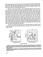
2.2.4 Calibration circuitry
Process variations influence device parameters, and hence matching-circuit behaviors. The
matching result, therefore, may lead to errors. The new calibration scheme shown in Figs. 6
and 7 has been developed to mitigate the errors caused by device mismatch. According to
the International Technology Roadmap for Semiconductors (ITRS-2008), transistor
90
μ
A
100
μ
A
110
μ
A
120
μ
A
130
μ
A
-0.5V
0
0.5V
ΔV=0.35V
Output current (
μ
A)
Δ
I
2
=11.4
μ
A
Δ
I
1
=10.5
μ
A
131
μ
A
125
μ
A
119.6
μ
A
114.5
μ
A
ERROR
2
= 0.9
μ
A
ERROR
1
= 119.6
μ
A-114.5
μ
A
=5.1
μ
A
Fig. 6. Two distance-evaluating methods. Curves were generated by a 5-interation post-
layout Monte Carlo simulation of a matching cell having random changes of 10% in
transistors’ length and width. The simulation was carried out at V
DD
= 3.3 V and V
ref
=1.65 V.
Highest and lowest current curves were focused on. For the same distance between the
input vector element and the template vector element, ΔV = 0.35 V, for example, the
conventional distance-evaluating method and the proposed method are demonstrated.
Solid State Circuits Technologies
32
I
1
I
2
I
64
Currents from matching cells for 1 vector
Current
memory
SW1
SW2
To WTA
I
1
I
2
I
64
Current
memory
SW1
SW2
V
X
-V
T
Memorized (phase 1)
X
ΔI
i
(phase 2)
∑
=
=
Δ=
64
1
)(
N
i
i
k
SCORE
II
I
peak(i)
I
out(i)
T
Phase 1
Phase 2
(a)
To WTA
I
1
I
2
I
64
SW1
SW2
From matching cells
V
DD
∑∑
==
−=
64
1
)(
)(
64
1
)(
)(
)(
i
k
iout
i
k
ipeak
k
III
SCORE
∑
=
64
1
)(
)(
i
k
ipeak
I
∑
=
64
1
)(
)(
i
k
iout
I
T
1
T
2
T
3
T
4
T
5
T
6
T
7
T
8
T
9
C
1
(b)
Fig. 7. Calibration scheme. (a) Calibration scheme operation. In phase 1, all peak output
currents are memorized in current memories. In phase 2, the similarities between the input
vector and the template vectors are evaluated. Only one current memory is required for one
vector-matching circuit. (b) Circuit diagram of the current memory and subtractor.
dimensions may vary above 10%. The small figure at the top left of Fig. 6 illustrates
matching-cell characteristics where the widths and the lengths of NMOS transistors of the
matching cell vary randomly up to 10% as a result of process variations. These
characteristics were obtained by a post-layout extracted circuit Monte Carlo simulation, and
we focus on the highest and the lowest current curves. For the same distance between the
input vector element and the template vector element, ΔV = 0.35 V, for example, two
distance-evaluating methods are shown in the remaining part of Fig. 6, which is an enlarged
Low-Power Analog Associative Processors Employing
Resonance-Type Current-Voltage Characteristics
33
image of the small rectangle at the top left. In the proposed method, the similarity is
determined by the difference between the peak current and the output current at the
moment of data matching. In the previous conventional approaches (Delbruck, 1991; Hasler
et al., 2002; Yamasaki & Shibata, 2003; Ogawa & Shibata, 2001; Peng et al., 2005), the output
current itself was utilized as the matching result. ERROR
2
(0.9 μA) and ERROR
1
(5.1 μA) in
the figure refer to errors caused by the former method and the latter one, respectively. It is
clearly shown that the proposed differential current method offers a better result. In order
to implement this method, peak currents are stored in current memories in phase 1 (the
writing phase), namely, at the time of template data download to matching cells. In phase 2
(the evaluation phase), differences between currents are obtained. Only phase 2 is repeated
for each new input vector. This scheme is shown in Fig. 7(a), and the circuit diagram of the
current memory and subtractor is presented in Fig. 7(b). The matching scores between input
vector and template vectors are calculated by eq. (3).
SCORE
64 64 64
() () () () ()
peak() out() peak() out()
111
kkk k k
ii i i
iii
III I I
===
=−=−
∑∑∑
(3)
According to this scheme, the greater similarity corresponds to the lower current rather than
the higher one in the previous approaches.
2.3 Experimental results
2.3.1 Chip fabrication
The proof-of-concept chip was designed and fabricated using 0.35-μm 2P3M CMOS
technology. The proposed matching-cell module includes 32 template vectors for the
purpose of demonstration. The mechanism is preserved even in the case of a larger number
of template vectors. The chip micrograph is shown in Fig. 8. The chip size is 4.9×4.9 mm
2
,
and the features of the chip are summarized in Table 1.
SRAM
Matching-cell array
Current memories
TWTA
Serial DACs + Voltage followers
Fig. 8. Micrograph of the proof-of-concept chip fabricated using 0.35-μm CMOS process.
Solid State Circuits Technologies
34
2.3.2 Measurement results and discussion
The measured characteristics of the vector element matching cell with various values of the
reference voltage are illustrated in Fig. 9.
Since the NMOS threshold voltage is around 0.6 V in
the 0.35-μm CMOS technology in which the test chip was fabricated,
it is shown that by
varying V
ref
from high to low values, the operation of the matching cell is altered from the
above-threshold regime to the subthreshold regime, respectively. When operating in the
subthreshold regime, the peak output current becomes as low as 80 nA at V
ref
of 0.4 V. The
results suggest an opportunity for building very low-power information processing systems.
Technology
2P3M 0.35-μm CMOS Process
Power supply (V) 3.3 (maximum)
Die size (mm
2
)
4.9 × 4.9
Number of vectors 32 vectors, 64 dimensions
Frequency (MHz) 33.3
Power consumption (mW) 21 at V
ref
= 0.55 V, V
DD
= 3 V, Clk = 33.3 MHz
Matching time (μs)
2.2 at 33.3 MHz
Table 1. Specifications of the proof-of-concept single-core chip.
740nA
280nA
80nA
7.5
μ
A
5.2
μ
A
3.2
μ
A
1.7
μ
A
0.74
μ
A
ΔV = V
X
-V
T
Vref=0.7V
Vref=0.65V
Vref=0.6V
Vref=0.55V
Vref=0.5V
Current
(1
μ
A/div)
0
0.5V
-0.5V
Vref=0.5V
Vref=0.45V
Vref=0.4V
Current
(100nA/div)
0
0.5V
-0.5V
ΔV
Vref=1.65V
0
Vref=0.75V
20μA/div
Output
current
(V)
-1.5
-1.0
-0.5
0.5
1.0
1.5
Fig. 9. Measured characteristics of the matching cell with various values of the reference
voltage.
Figure 10 illustrates the experimental results for handwritten digit recognition utilizing the
proposed architecture, as a simple demonstration. The digits “0”-“9” were converted to
Low-Power Analog Associative Processors Employing
Resonance-Type Current-Voltage Characteristics
35
PPED vectors so as to play the role of template vectors. The twenty-two other template
vectors were dummy vectors. Then, the PPED vector of the handwritten digit “9” was
employed as the input vector. The winner address shown in Fig. 10(a) corresponds to the
location of the digit “9”. This result verifies correct chip operation. Figures 10 (a) and 10 (b)
Template vectors
Input vector
Searching the winner
Writing templates and
Inputting handwritten “9” digit
Winner Address
Common Ramp signal
"Winner found" signal,
a rise from 0 to VDD indicates
that winner was found.
Winner address=09H
Starting to find winner
Winner found
Ready for next matching
1
1
1
1
1
Address lines are reset to 1
1
0
0
1
0
LSB
MSB
(a)
Bit 0
(LSB)
Bit 1
Bit 2
Winner address
"Winner found" signal
Winner found
(b)
Fig. 10. Demonstration of the whole system operation. (a) Waveforms obtained with a logic
scope describe the chip operation at 1 MHz for the purpose of illustration. The operating
frequency is low because of the resolution limitation of the logic scope. (b) Waveforms
obtained using an oscilloscope verify the chip operation at the frequency of 33.3 MHz
Solid State Circuits Technologies
36
show the waveforms captured from a logic scope and an oscilloscope, respectively. Since 72
clock cycles, comprising 8 cycles for SDAC and 64 cycles for an off-chip digital- to-analog
converter utilized as the ramp-signal generator for the WTA circuit, are required to finish a
template-matching cycle, the search time in this experiment is 2.2 μs at the frequency of 33.3
MHz and depends strongly on the speed of the ramp-up voltage signal employed in the
current-to-delay-time converter. The system was set up to operate at the supply voltage of
3.0 V and the reference voltage of 0.55 V. As a result, the average power dissipation of the
whole chip was about 21 mW.
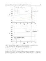
Moreover, in Fig. 11, the average supply current of the whole chip, including the matching-
cell array, the SRAM module, SDACs, voltage buffers, current memories, the WTA circuit,
and I/O pads, measured with various V
ref
’s is reported. The curves inherit the NMOS I-V
characteristics owing to the NMOS-based matching-cell architecture. It can be observed that
low supply currents are obtained with values of V
ref
below the threshold voltage. These low
reference voltages enable matching cells to operate in the subthreshold regime, in which the
matching cell output currents drop exponentially with decreasing V
ref
. As a result, the
matching-cell array consumes very low power. Since the measured currents are for both the
matching-cell array and the other parts, the supply currents in the subthreshold region
remain at certain values rather than very low ones. These currents are mainly for the other
parts whose power dissipations are reduced when lowering the supply voltage, and are
independent of V
ref
. Consequently, the supply currents are approximately constant values in
the subthreshold region, as shown in Fig. 11.
0
20
40
60
80
100
120
140
160
0 0.5 1 1.5 2
VDD=3.3V
VDD=3.0V
Vref(V)
Current (mA)
Fig. 11. Relationship between V
ref
and supply current.
The performance of the associative processor is summarized with some others from the
literature in Table 2. Because the time-domain WTA is utilized in this work because of its
simple architecture, the search time is quite long compared with those of digital
implementation (Nakata et al., 1999)
and mixed signal implementation (Abedin et al., 2007).
In addition to the matching-cell array, the WTA plays an important role in the power-saving
scheme because the power consumption of the WTA increases significantly upon increasing
the number of template vectors. In the present chip, the optimization of the speed and
power dissipation of the WTA has not been considered. In order to make the proposed
architecture practical and much better than digital approaches, a low power WTA would be
considered in future studies. Furthermore, although analog flash implementation (Kramer et
Low-Power Analog Associative Processors Employing
Resonance-Type Current-Voltage Characteristics
37
al., 1997) offers very low power consumption, such an implementation requires particular
mechanisms in the template-writing phase, making the flash implementation difficult to
control and hence, flexible programmability difficult to realize.
Technol.
Power consumption
(mW)
Matching
time (μs)
Estimated
power/MC
(mW)
This work Analog
21
(32 vectors, 64 elements)
2.2
0.01
Tuttle, et al.
1993
Analog
50
*)
(256 vectors, 16 elements)
2
0.012
Kramer, et al.
1997
Analog
flash
195
(4K vectors, 64 elements)
4.6 0.00074
Oike, et al.
2004a
Digital
320.7 at V
DD
=1.8V
15.1 at V
DD
=0.9V
(64 vectors, 32 elements)
2
∼8.12
0.157
0.0074
Nakada, et al.
1999
Digital
290
(256 vectors, 16 elements)
1.1 0.071
Abedin, et al.
2007
Mixed
signal
195
(64 vectors, 16 elements)
0.16 0.19
Table 2. Performance comparison.
*)
Not including power for memory and D/A converters.
3. Extension to a multi-core/multi-chip architecture of associative processors
3.1 Multi-core/Multi-chip configuration
In this session, a solution to how the system is hierarchically scaled up to a vast scale
integration is presented. For a vast scale integrated system, a large number of template data
can be implemented in multiple associative processors, thus making the recognition system
more intelligent. In this regard, a multi-core/multi-chip architecture of associative
processors has been developed (Bui & Shibata, 2008b; 2009).
In the literature, several multi-chip architectures based on all-digital technology have also
been introduced (Nakata et al., 1999; Oike et al., 2004b). Although these systems offer
accuracy, they occupy large chip real estate and usually have complicated structures. On the
contrary, analog-technology-based system employing time-domain winner-take-all (WTA)
is introduced in this study. The multi-core/multi-chip architecture inherits the architecture
developed for the fully parallel single-core associative processor described in the previsous
session. The problem associated with inter-chip communication delay which is critical in the
time-domain WTA operation has been resolved by a newly-developed winner-code-decision
scheme. In addition, switched-current technology has been utilized so as to further reduce
the power consumption.
The block diagram of a multi-core/multi-chip associative system is shown Fig. 12. In
general, the system includes many chips, and each chip itself has many cores. For the
purpose of demonstration, the poof-of-concept system in this study is composed of four
associative chips, namely, one master chip and three slave chips. Each chip consists of four
Solid State Circuits Technologies
38
32-vector cores. (Each vector has 64 elements of 8-bit numbers.) As a result, a 512-vector
associative system is constructed as a demonstration. The master chip and the slave chips
are designed in the same configuration. They play master/slave roles when they are
combined to form the whole system and operate in parallel. The master chip is
distinguished from other slave chips by activating an additional majority-code-decision
circuit described in the following section. Employing many cores on a single chip reduces
the time required for downloading the information of template vectors stored in SRAMs to
analog matching-cell arrays. In addition, four cores are activated separately, thus they can
do matching operations independently or as a whole large system.
The 32-vector single-core architecture was already described in the previous section. In each
core, template vectors are stored in on-chip digital memory, namely SRAM in the design.
Employing digital memories is an inexpensive solution instead of using high-cost analog
nonvolatile memory technologies. And compact serial digital-to-analog converters (SDACs)
are used to convert digital values to analog voltages prior to similarity evaluation
processing. The similarity evaluation between the input vector and template vectors is
carried out in parallel by vector-matching circuits, each of which consists of 64 bell-shaped
vector-element matching cells (MCs), a current memory, and a current subtractor as shown
in Fig. 13. Signals WR and RD in Fig. 13 correspond to WRITE control signal and READ
control signal, respectively. These signals permit to store matching results represented by
currents into the current memories and to read out the matching scores from the subtractors.
As mentioned in Section 2, current memory plays an important role in the device-mismatch
calibration scheme in which the similarity is determined by the difference between the peak
current and the output current at the moment of similarity evaluation. In the study,
switched-current technology is employed to control RD and WR signals in order to cut-off
currents flowing in the vector-matching circuits as well as the current memories except
moments of downloading template vectors to the matching-cell arrays and evaluating
similarities. As a result, the power dissipation is reduced further as compared with the
design in Section 2.
SYSTEM BUS
WTA 2
MUX
3
-
State buffer
ENBL
Master chip (chip #0)
Winner signal
Winner signal
Winner Address
WTA3
Chip1
Chip2
Chip3
Chip0
Majority-code
-decision circuit
Enable
signals
Winner
addresses
WTA 2
MUX
3
-
State buffer
Slave chip (chip #1)
WTA1
WTA3
INPUT VECTOR
WTA1
Matching-Cell
Array
WTA1
SRAM
D/A Converters
Matching-Cell
Array
WTA1
SRAM
D/A Converters
Core #0
Matching-Cell
Array
WTA1
SRAM
D/A Converters
Matching-Cell
Array
WTA1
SRAM
D/A Converters
WTA1 WTA1
Core #1Core #2
Core #3
Core #0Core #1Core #2Core #3
Activated
Activated
ADDR[4-0]
ADDR[6-5]
WTA3_OUT[1-0]
WTA3_WFND
CHIP_WFND
ADDR[8-7]
Fig. 12. Block diagram of the multi-core/multi-chip architecture.
Low-Power Analog Associative Processors Employing
Resonance-Type Current-Voltage Characteristics
39
V
GG
SW
V
ref
T1
T2
T3
T4
C1
C2
I
out
1
I
out
64
To Current-to-Delay-
Time Converter
WR
RD
C
1
∑∑
==
−=
64
1
)(
)(
64
1
)(
)(
)(
i
k
iout
i
k
ipeak
k
III
SCORE
Subtractor
1
0
WR
RD
R/W
R/W
One vector-matching circuit
W/L
W/L
20W/L
Current memory and subtractor
RD
One vector-element matching cell
SEL
SEL
V
1
V
2
T5
T6
T7 T8
T9
T10
T11
T12
T13
T14
T15
T16
T17 T18
Temporary
floating gate
Current memory
Fig. 13. Schematic of a vector-matching circuit.
Multi-core/Multi-chip configuration
The global winner, namely the template vector having the minimum distance to the input
vector is searched for through a three-stage WTA circuit. Each WTA stage employing a
time-domain WTA (Ito et al., 2001) senses the first up-setting signal among inputs and
generates the binary address representing the location of the winner. The winner signal is
also passed to the next WTA stage. In this manner, WTA1 searches for the local winner
inside the 32-vector matching-cell array, WTA2 searches for the winner of one chip, and
WTA3 searches for the global winner which is the winner when combining various chips
together. All three WTA stages and the majority-code-decision circuit described below are
layouted on each chip. The configuration is illustrated in Fig. 12.
However, when integrating several chips to form a larger system, signal propagation delays
occurring in long inter-chip interconnects may lead to errors in time-domain signals. This
will result in the decision error of the final WTA’s (WTA3’s). In order to deal with this
problem, a balanced architecture should be satisfied to equalize delay times of inter-
connection signals. However, even though with the balanced architecture, different
propagation delays may still occur. Because of this problem, a redundant circuit following
the final stage WTA, called the majority-code-decision circuit, has been developed. This
circuit is only activated on the master chip. The circuit makes the decision based on the
winner address codes generated by all WTA3’s. The block diagram of the circuit is shown in
Fig. 14. Basically, it consists of a binary counter, binary comparators, and a majority voting
circuit (MVC). In the proof-of-concept chip, they are a 2-bit counter, 2-bit comparators, and a
three-of-four MVC, respectively. As a result, the global result becomes more reliable than
the architecture without a majority-code-decision circuit. In the case of a 2-bit 4-input
majority-code-decision circuit like that in this study, the circuit can be constructed by
combining two three-of-four MVCs whose outputs form the 2-bit majority winner code; but
Solid State Circuits Technologies
40
it is not the general case. It means that such architecture is not correct for other cases whose
winner codes are larger than two bits. On the contrary, the method developed in this study
is general and suitable for any case. The counter counts up from zero when it is activated;
the winner-indicating-signal (ADDR_FND) indicates whether the majority winner code is
found. This signal goes high when output of the counter coincides with the majority winner
code.
COUNTER
CLK
MAJORITY VOTING CIRCUIT
DECODER
To 3-STATE BUFFERS
On Master chip (chip #0)
Highest
addresses
Enable
WINNER ADDRESS FOUND
2-bit
COMPARATOR
2-bit
COMPARATOR
2-bit
COMPARATOR
2-bit
COMPARATOR
Winner signal
WTA3
Chip 0
Winner signal
WTA3
WTA3 WTA3
Chip 1
Winner signal
Chip 2
Winner signal
Chip 3
Winner signal
Chip 0
Winner signal
Chip 1
Winner signal
Chip 2
Winner signal
Chip 3
Winner signal
On chip #0
On chip #1
On chip #2 On Chip #3
Winner Address
Code from Chip 0
ADDR[8-7] ADDR_FND
CHIP_ENBL 0
CHIP_ENBL 1
CHIP_ENBL 2
CHIP_ENBL 3
WTA3_WFND
Winner Address
Code from Chip 1
Winner Address
Code from Chip 2
Winner Address
Code from Chip 3
Fig. 14. WTA3 and the majority-code-decision circuitry.
V
out
V
RAMP
Cut-off signal
WTA1
Time-Domain
WTA
Winner signals
t
V
t
V
I
SCORE
(k)
I
SCORE
(k)
(k)
Core #0
Core # 1
Core #2
Core #3
Current-to-Delay-
Time Converter
t
V
Fig. 15. Current-to-delay-time converter.
Low-Power Analog Associative Processors Employing
Resonance-Type Current-Voltage Characteristics
41
In addition, in order to further reduce the power dissipation, switched-current technology is
also utilized in the current-to-delay-time converters by the method illustrated in Fig. 15.
Winner signals obtained by WTA1’s are combined by an OR-gate; the output signal is
employed as a cut-off signal disconnecting both the common ramp voltage signal and score
currents from current-to-delay-time converters. In this manner, once the winner signal is
found by one of WTA1’s, all current-to-delay-time converters are deactivated, thus further
reducing the power consumption. This method can be applied to any large matching-cell
array by dividing the array into several smaller blocks.
3.2 Experimental results
3.2.1 Chip fabrication
Measurement results obtained from the previous single-core chip fabricated in a 0.35-μm
double-poly triple-metal CMOS technology have been discussed in Section 2. As an
extended research, a proof-of-concept chip consisting of four cores was designed and
fabricated in a 0.18-μm 5-metal CMOS technology. Figure 16 shows a micrograph of the test
chip, and layout of a matching cell is shown in Fig. 17. Each core including a memory
module and a matching-cell module occupies an area of 1760 μm × 570 μm. The size of
matching cell is 19.7 μm × 7 μm. It should be noted again that the CMOS inverter-based
matching cell presented in (Yamasaki & Shibata, 2003) is larger than the present cell due to
the N-well region required for implementing PMOS transistors. This is an advantage of pure
NMOS configuration. However, the present matching cell size is still large due to the large
area required for capacitor layout. The specifications of the proof-of-concept chip are
summarized in Table 3.
SRAM
WTA2
WTA3 &
Majority-Code-Decision
1760 μm
570 μm
Matching-Cell
Module
Fig. 16. Micrograph of the proof-of-concept chip fabricated using 0.18-μm CMOS process.
Solid State Circuits Technologies
42
Fig. 17. Micrograph of a matching-cell module and layout of a matching cell (MC).
Technology
1P5M 0.18-μm CMOS
Power supply (V) 1.8
Core size (mm
2
)
1.76 × 0.57
Matching cell size (μm
2
) 19.7 × 7
Search time (μs)
8.16 at clock frequency = 16.7MHz
( Incl. 8 clocks for SDAC and 128 clocks for the ramp voltage)
Power consumption (mW)
1.17 mW/32-vector matching-cell module; 6.48 mW/chip
when operating in the subthreshold region with V
DD
=1.8 V.
Function
128 vectors/chip, 512 vectors/4-chip system.
Nearest match identification.
Table 3. Specifications of the proof-of-concept chip.
3.2.2 Measurement results
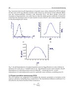
Figure 18(a) shows the characteristics of matching-cell measured with some small reference
voltages. For the 0.18-μm CMOS technology in which the prototype chip has been
fabricated, the threshold voltage of NMOS is around 0.45 V. As can be seen in the figure, in
the subthreshold regime, the peak current of the matching cell characteristics is reduced to
only several tens of nA. This is an important issue in power-saving schemes. The entire
Low-Power Analog Associative Processors Employing
Resonance-Type Current-Voltage Characteristics
43
curve of peak output current with respect to the reference voltage shown in Fig. 18(b) has
the shape of NMOS transistor characteristics.
Fig. 18. Measured matching cell characteristics.
In Fig. 19, the average current of the whole chip including four cores and chip-I/O buffers
and the current in a single 32-vector matching-cell module measured with various V
ref
’s are
reported. As can be seen from the figure, the curves have the shape of the NMOS I-V
characteristics owing to the NMOS-based matching-cell architecture. In the subthreshold
region, the current of the entire chip and that of one matching-cell module are 3.6 mA and
0.65 mA, respectively. As a result, the power consumption per matching cell is reduced to as
small as 0.79 μW.
0
5
10
15
20
25
30
35
40
00.10.20.30.40.50.60.70.80.91
Vref (V)
Current (mA)
One chip
One matching-cell module
0.65mA
3.6mA
Fig. 19. Measured current as a function of the reference voltage V
ref
.
Figure 20 (a) shows measured signals CHIP_WFND and WTA3_WFND generated by the
WTA2 and WTA3 on the master chip, respectively. Waveforms at the output of the majority-
code-decision circuit measured by an oscilloscope are shown in Fig. 20(b). The signal
WTA3_WFND generated by WTA3 is employed as the control signal enabling the operation
Solid State Circuits Technologies
44
of the counter in Fig. 14. When the winner is found by the WTA3 on the master chip, the
counter is activated, and begins to count up. When the counter output, ADDR[8-7],
coincides with the majority winner code, ADDR_FND signal goes high, indicating that the
majority code was found and available on address lines ADDR[8-7]. This signal also stops
the counter counting. In the demonstration, the majority winner code is 10
2
corresponding
to chip #2. Majority-making-decision principle plays an important role not only in this
design of a multi-chip architecture but also in miniscule-device-based designs where the
device parameter variability is an important issue.
Fig. 20. Measured waveforms of the majority-code-decision circuit operating at a clock
frequency of 20 MHz.
Demonstration of the whole system operation is illustrated in Fig. 21. All vectors of the test
chip were assigned with given data. Required signals were connected to illustrate a system
consisting four chips. After all template vectors were temporarily memorized inside matching-
cell arrays, two input vectors were applied to the system input successively for matching. In
Fig. 21, which is the measurement result captured from a logic scope, address lines ADDR[4-0],
ADDR[6-5], and ADDR[8-7] represent winner address codes generated by WTA1, WTA2, and
the majority-code-decision circuit, respectively. Namely, they are the winner template vector
inside the winner core, the winner core inside the winner chip, and the winner chip of the
multi-chip configuration, respectively. As a result, the global winner address is the
combination of these three address codes. In this demonstration, the global winner addresses
captured on the system bus are “100000101
2
” representing the global winner is vector #5
(00101
2
) of core #0 (00
2
) in chip #2 (10
2
) and “101010111
2
” representing the global winner is
vector #23 (10111
2
) of core #2 (10
2
) in chip #2 (10
2
), respectively. WTA_EVAL signal enables the
operation of the three-stage WTA circuitry. When this signal goes high, it also enables an off-
chip ADC to generate the common ramp voltage used in current-to-delay-time converters.
GLOBAL_WFND signal indicates that the winner template vector has been found and its
address is available on the system bus. This signal also latches the global winner addresses on
the system bus. The experimental results verify the correct operation of the system.
Low-Power Analog Associative Processors Employing
Resonance-Type Current-Voltage Characteristics
45
A searching cycle finishes in 136 clock cycles including eight clocks for on-chip D/A
conversion of an input vector and 128 clocks for off-chip ramp voltage generation. In
addition, employing many cores on a single chip reduces the time required for downloading
the information of template vectors to analog matching-cell arrays.
Fig. 21. Demonstration of the whole system operation by waveforms captured by a logic
scope.
4. Conclusion
In this chapter, a methodology for building a low-power high-capacity associative system
has been presented. Device mismatch problems as well as decision errors associated with
inter-chip communication delays have been resolved by introducing the calibration scheme
and the majority-code-decision circuit. Because of employing bell-shaped matching cell as
similarity/dissimilarity-evaluation element, this study, therefore, provides an intermediary
stage connecting CMOS designs and the coming era of nano devices. This is because such
resonance-type current-voltage characteristics are typical characteristics often observed in
nano-scale devices. The system also has the possibility of a large database capacity by
employing the multi-core/multi-chip architecture. In principle, search time is independent
of the number of cores as well as the number of chips. The operation of the systems as well