Frontiers in Guided Wave Optics and Optoelectronics Part 9 ppt
Bạn đang xem bản rút gọn của tài liệu. Xem và tải ngay bản đầy đủ của tài liệu tại đây (2.9 MB, 40 trang )
Advances in Femtosecond Micromachining and Inscription of Micro and Nano Photonic Devices
305
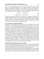
will not be covered here but may be found in references (T. Südmeyer, 2008; S. Backus,
1998), however, differences in terms of the output pulses will be discussed.
The wavelength ranges of the types of laser are determined by a number of factors. There
are two main bands covered by the fibre lasers at 1030-1045nm and around 1550-1560nm.
The two bands correspond to the dopant used in the lasers cavities. The conventional C-
band erbium window is at 1530-1565nm and ytterbium sources operate at around 1030-
1050nm (S. B. Poole, 1985). There is a third much smaller group of fibre lasers operating at
around 800nm. Bulk amplifiers and oscillators, are also governed by the amplification
material chosen. They typically use Ti:Sapphire and ytterbium and as such commonly
operate at wavelengths around 800nm and 1030-1050nm.
The energy per pulse is a parameter to be considered in a similar way to the peak power.
The pulse energy required will depend on both the material and the chosen application.
Machining of a crystal for instance will typically require a much greater energy per pulse,
for example energies up to and above 80 Jcm
-2
(T. V. Kononenko et al., 2008) for natural
diamond, while for index change in PMMA energies above 0.6 Jcm
-2
(A. Baum et al., 2007)
cause permanent change. The energy per pulse of the types of laser are detailed in table 1.
The oscillators typically have energies in the range of 1-100s nJ per pulse, whereas the fibre
lasers offer energies in the μJ range and amplifier pulse energies typically fall in the mJ
range. The choice of pulse energy for a given application is critical as most materials have a
small window of energies between the desired effect, say index change, and damage. The
other consideration is that to control the energy, and other parameters, incident on a sample
is significantly easier when not having to operate at the extreme limits of attenuators or with
insufficient laser energy after the losses experienced through the system.
Table 1. Table showing the market survey of femtosecond sources and basic properties
Frontiers in Guided Wave Optics and Optoelectronics
306
Femtosecond pulses are considered ultrashort and as table 1 shows they range greatly in
practical terms. There are effectively two or three classifications of pulse duration. There are
the extremely short pulsed lasers, with pulses typically in the 10s of femtosecond duration
which are most commonly, although not exclusively, oscillator lasers. The next region is
about 100-350 fs that are often amplifier lasers. The final group is from 350-800 fs and is
largely occupied by fibre and amplifier lasers. The pulse duration makes a significant
difference to the pulse-material interaction and the pulse energy required.
Repetition rates of commercially available systems range greatly from single kHz through to
100MHz. The range leads to a significant difference in the applications of each. There is
some evidence to suggest that better quality waveguides, for instance, are written with
lasers operating in the MHz regime rather than kHz (S. M. Eaton et al., 2005). On the
contrary often for micro-machining ablation lower repetition rates in the 1-300 kHz range
tend to be chosen because they have higher pulse energies which are above the ablation
threshold. For these lower repetition rate systems there is also less thermal loading due to
the pulse train spacing. Repetition rates and the resultant thermal loading, or absence, offers
clear advantages of one repetition rate over another for a specific task.
In conclusion the parameters of a chosen laser will strongly influence the effectiveness of
work in particular area. The parameter windows are relatively small for high quality results
in any given application.
5. Techniques employed
There are several different techniques employed when making micro-machined devices
through inscription and ablation. Some of them are techniques applied to both regimes and
others are applied more specifically to one or the other. Typically using a laser to perform
micro-machining involves complex physical processes and is dependent on fine parameters
of the material and laser. Theoretical models exist and are touched upon in other sections of
this chapter, however, they are often considered to be only a guideline and require
refinement for optimal processing when using a practical system. In this section some of the
basic methods and techniques applied to micro-machining are explained.
5.1 The basic system
Systems tend to either operate by having the sample fixed and the laser beam moving or by
fixing the sample to a moving stage, or set thereof, and having a fixed objective lens, figure
5. There is also the option to use galvanometric systems where the beam is manipulated
using mirror(s) and obviously a combination of all three. Each of the layouts has its own
pros and cons depending on the main purpose of use, for instance when the desired sample
is small and is required to be machined quickly then galvanometric systems can be most
advantageous, however, when operating over a larger area these systems suffer from
spherical plane effects and correcting for these often leads to a loss of sharpness in the
focusing. This is especially important for femtosecond work where the depth of focus, due
to the nonlinear nature, is so small.
Often the most practical systems use a partially fixed objective, where the objective is also
on a stage but often remains stationary when working at a given depth in the sample, and
use mechanical or air bearing stages to move the sample. These are often programmed by
computer linked drive control units. The majority of stages operate some version of CNC
(Computer Numerical Control) system (Smid, 2005) each of which have their own protocols,
however, the techniques used are applicable to most if not all systems of this sort.
Advances in Femtosecond Micromachining and Inscription of Micro and Nano Photonic Devices
307
Fig. 5. A schematic of three types of focusing arrangement from left to right a static sample
with moving objective, a moving stage with static objective lens and a galvanometric set up
with motion controlled by mirror angle.
5.2 Common terminology & basic techniques
There are a number of terms applied to certain types of machining that describe the
fundamental technique applied to working on a work piece and these are defined in table 2.
The first of which we will consider is percussion drilling. This is a process of firing a number
of pulses on a given area, each pulse removing a very small volume of material, thus leading
to the creation of a hole. Typical laser repetition rates over 1kHz allow removal rates to be
viable for use. This technique is used for the creation of small holes through or in materials.
In general the material removal rates are relatively constant for small depths (to ~100 μm)
after which the removal rate operates as the square root of the depth. Thus the time taken to
double the depth is typically in excess of four times that of the initial hole. This occurs
because as the beam penetrates to the bottom of a hole energy is lost to the material and the
nature of Gaussian beam paths, after focusing, means that the energy available at the bottom
decreases as the wing that is clipped is inversely proportional to the aspect ratio increase.
Typically helical trepanning produces some of the smoothest side walls and most uniform
holes but takes longer and tends to be best applied to smaller artefacts.
5.3 Other considerations
There are a number of other parameters and components to be aware of that can be critical
to the finish and quality of a desired object. It is important to consider the desired aspect
ratio or etch depth, the NA and working distance of the lens, the position of the focus in the
sample, the beam polarisation, the speed of the moving parts and an inspection mechanism.
The aspect ratio is defined by the ratio of depth to width of an artefact, for example, a
microfluidic channel or hole through a ceramic. The etch depth is the effective write depth
of an inscribed feature such as a waveguide or diffractive element inside the bulk of the
material. To optimise both of these parameters the choice of lens, power and beam shaping
are fundamental. If aiming to write a deep slot into a substrate one would typically choose a
lens with a low NA and long working distance so that it could operate at a distance and
over a range of positions without being coated with the debris created by the plasma and
Frontiers in Guided Wave Optics and Optoelectronics
308
Single shot drilling - The process of using a single laser pulse to drill, this is
rarely used.
Percussion drilling - The use of a number of laser pulses at a repetition rate
spacing above that of the length of the pulse used to remove material. Can lead
to surface spatter which can lead to micro-cracking, deformation of hole shape
and achieving high aspect ratios is often difficult.
Trepanning - This is essentially percussion drilling with circular motion, often
a pilot hole is drilled and then a spiral motion followed by circular finishing.
The technique suffers from the same drawbacks as percussion drilling. The
hole size formed by this motion is, to within the radius of the plasma, the
diameter of motion. The holes produced by trepanning are generally more
circular and accurate than a percussion drilled hole, however, they are larger in
size.
Helical drilling - The process of quantizing the ablation steps reaching
breakthrough only after a number of passes described by a spiral motion. This
often has a more circular geometry than trepanning and also minimises the
load placed on the opposite face to that of the focus. It tends to also give less
recast, however, takes significantly longer to process.
Cutting - Cutting through a sample using a series of pulses through motion of
the beam or sample, often multiple passes are required.
Etching / Milling - Removing a defined depth of material through control of
pulse energy and/or number of pulses per location.
Rastering - The motion of moving back and forth over an area with lines
separated by a given pitch. By varying the pitch this can lead to the removal of
material from an area or in trenches. Typically these form square wave patterns
although other forms are also used.
Table 2. A Table of the common techniques and a brief description of their mechanism.
avoiding contact with the material. Ideally most of the work should be done with a static z
component and the right choice of lens, however, there are times when stepping the lens
towards the sample is necessary to achieve a specific depth or profile. The position of the
focus required to ablate a slot, when scanning, is typically not at the midpoint of the desired
slot depth. Through experience it comes out at typically 1/3 of the depth but the exact
position will change depending on the sample and other parameters. There are also issues to
do with shielding by the walls when looking to achieve high aspect ratio side walls. This is
because the pulses wings are clipped reducing the power of the pulse.
The speed of any scanned motion, as with repetition rate, will affect the rate of removal of
material. This is because the fluence will be varied by the change in the speed of motion as
the number of pulses per unit volume will be less. A variation in the repetition rate would
have the converse effect. That is to say that if the pulse rate increases by a factor of 2 that the
removal rate would increase linearly, assuming constant pulse energy. Whereas a doubling
of the speed would half the removal rate or create a series of dots rather than a line.
Advances in Femtosecond Micromachining and Inscription of Micro and Nano Photonic Devices
309
There are two types of polarisation that can be used, linear and circular polarisation. The
polarisation is believed to affect the write quality of inscribed lines such as waveguides. The
current thinking is that a polarisation orthogonal to the direction of write for straight
waveguides, or circular for curved ones, is preferable and results in smoother tracks (M.
Ams et al., 2006). Polarisation parallel to the direction of write is not favourable since it
produces less smooth tracks. There are other techniques employed such as combining
cylindrical lenses with the regular microscope objectives to refine the width of written lines.
The ability to fully inspect and align a sample pre- and post-inscription or ablation is of
fundamental advantage to any system. The use of confocal systems and inspection methods
to inspect during writing has also developed considerably in recent years (J. Li, et al., 2008).
A standalone camera can also be used to monitor the sample. The exact design and
components used will not be uniform across all systems but the importance and advantage
gained by their inclusion are extremely significant to the complexity of the fabricated
devices.
Some examples of femtosecond micromachining are shown in figure 6. The images illustrate
some of the common effects observed, both good and bad, from femtosecond
micromachining. By reducing the separation between the slots it is possible to reduce the
wall thickness and create extremely high aspect ratio structures. Figure 6 also shows entry
and exit holes. The entry holes in this example are slightly rounded which can be corrected
for by adjusting the focus position. The third image shows how both good and bad set up
parameters affect the resultant finish quality.
Fig. 6. Slots machined in stainless steel shim 0.178 mm thick; (LHS) entry side showing
gradual reduction in slot separation, (left middle) exit of the same slots, (right middle) slot
showing what happens when the parameters and finishing are correct and wrong, (RHS)
showing the high aspect ratio structures remaining after ablation.
5.4 Computer Aided Design (CAD) & rapid prototyping
There are a number of applications of femtosecond micro-machining where the complexity
and rapid prototyping required are less suited to programming the motion line by line. This
is clearly shown in the complexity of the microfluidic device illustrated by figure 7 below.
To code this line by line would be extremely time consuming and to change something like
the machining pitch could take considerable effort going through the code line by line. In
these situations the use of CAD software packages can be a significant advantage in being
able to vary the parameters (such as pitch, write speed and scaling) quickly and design
complex structures that would otherwise take significantly longer. Although it is not
impossible to code some of the more complex structures the plausibility and economy of
Frontiers in Guided Wave Optics and Optoelectronics
310
doing so when the software packages are available becomes more weighted in favour of the
automated approach (G. Smith, 2008).
Fig. 7. Computer Aided design images, from left to right 1) An plan view of a computer
designed microfluidic device, 2) the machine path lines shown for workpiece with green
representing the path of the laser ablation and red being the skimming non ablation transit,
3) a close up of the tool path for ablation showing rastering and a finishing edge pass.
5.5 Post processing
There are a few post processing techniques that are important in relation to femtosecond
micromachining. The most common technique is to wet etch using either hydrofluoric acid
(commonly abbreviated to HF and is hydrogen fluoride in water solution) or ammonium
bifluoride (ABF is chemically NH
4
HF
2
and a diluted version of HF in a salt form, although
used in water solution). The whole process involves inscribing the material (below the
ablation threshold) using the laser focal spot then placing the substrate in the acid. The acid
preferentially etches the inscribed areas at a rate of 50:1 in fused silica (K. Sugioka et al.,
2007) and as such removes the inscribed area selectively. This technique offers the ability to
make smoother structures in transparent materials with smaller features and higher aspect
ratios. It is also possible to fabricate subsurface channels that would otherwise take a
sequence of layer deposition stages or lithographic techniques. There is a downside, in that
the use of these chemicals adds additional processes and time over direct ablation and
involves the handling of hazardous chemicals. Figure 8 shows work done in optical fibre.
The fibre has been exposed by femtosecond laser inscription below the damage threshold
then wet etched using HF producing very narrow, high aspect ratio channels through the
fibre core.
The use of heat treatment, cycled and constant, may be important for femtosecond
micromachined structures. In theory, the thermally induced stresses created by the
shockwaves propagating in the material around the plasma can be thermally annealed out
through heating the substrates post inscription. Heat treatment thermally relaxes the
material such that the stress is released and the permanent change of the inscription is all
that is left. This effect is still the subject of study and its ability to offer further
understanding of the plasma-material interaction will most likely be of fundamental impact
(S. Juodkazis et al., 2004).
Advances in Femtosecond Micromachining and Inscription of Micro and Nano Photonic Devices
311
Fig. 8. Micro-channels fabricated in standard fibre using fs inscription and chemical etching
(Y. Lai et al., 2006).
6. Applications
The numerous properties of femtosecond pulse interactions with a range of materials have
led to a diverse range of novel applications. For example, the ability to micromachine in 3
dimensions in transparent media due to the nonlinear interaction has opened up
possibilities that were previously not available without the addition of dopants and short
wavelength laser exposure. There are also a number of applications that would simply not
be possible without the use of femtosecond lasers for micromachining. Having said this
there should be a note of caution as while there are numerous advantages to the technology
it should not be considered as the only solution to all applications. Instead the advantages
should be utilised for specific purposes.
6.1 Periodic structures
Because of the short pulse duration and the high refractive index changes that can be
induced femtosecond lasers can be used to produce period structures in transparent
materials. More specifically, they have been used to fabricate fibre Bragg gratings (Y. Kondo
et al., 1999). These structures are written into or near the core of an optical fibre and reflect
light at a wavelength determined by the periodicity of the structure.
Two approaches to the fabrication of these structures have been optimised over the last few
years in the femtosecond domain: the point-by-point method (E. Wikszak et al., 2004; A.
Martinez et al., 2004, K. Kalli et al., 2009) and the phase mask method (K. A. Zagorul'ko et al.,
2003). Both methods had previously been used for the UV fabrication (with either CW or
conventional pulsed lasers) of fibre Bragg gratings however the femtosecond regime provides
some key differences due mainly to the localisation of the fringes which allows, for example,
multiple gratings to be positioned in unique positions around a single core, as shown in figure
9. This can be highly advantageous from a device design point of view as, for example, it
enables the production of a single fibre Bragg grating device that can be used as a directional
bend sensor. Gratings can also be inscribed through the hole structure of microsctructure
optical fibres using femtosecond lasers. Kalli et al have shown that with a suitable fibre design
it is possible to use femtosecond pulses to penetrate the holes of the microstructure fibre
without significant breakup of the femtosecond laser pulse during inscription.
Frontiers in Guided Wave Optics and Optoelectronics
312
In planar samples femtosecond lasers have been used to inscribe diffraction gratings which
can in turn be used to fabricate fibre Bragg gratings (G. N. Smith et al., 2009). A photograph
of one of these is shown in figure 9 showing first, second and third order phase masks. The
work to date demonstrates the proof of concept and flexibility for the use of femtosecond
lasers to make complex and reproducible phase masks. This approach has the potential to
rival e-beam fabrication of phase masks and has the advantage of being a single step
fabrication process that uses no chemicals.
Fig. 9. Femtosecond inscribed fibre Bragg gratings in (LHS) the centre of the fibre core and
(middle) on the edge of the fibre core, (RHS) photograph of a femtosecond phase mask
inscribed with fs laser underneath the surface of the UV grade fused silica (G. N. Smith et
al., 2009).
6.2 Micromachining of planar glass
Microfluidic device, incorporating high aspect ratio micron scale channels, can be directly
machined. These devices are developed as lab-on-chip devices for purposes such as
measuring a specific particle to particulate sorting and counting (D. N. Schafer, 2009). The
advantage is that they only require tiny amounts of a fluid to function thus reducing costs of
development of chemicals, allowing more information to come from smaller samples at
increased speed of prototyping and development. Some of typical structures that are
employed are shown in figure 10. They show bends, micropump holes, joints and high
aspect ratio structures in both planar and fibre samples all of which can be easily adapted
and machined using femtosecond micromachining giving advantages for rapid prototyping
(G. Smith et al., 2008).
There are a number of methods for making these devices. The most common is to inscribe a
structure in the material and then expose it to hydrofluoric acid. Another is to ablate
structures or create voids in the presence of what are known as wetting fluids (Y. Iga et al.,
2004). This works in the same way as you would use fluid with a standard milling process to
remove the debris from a machined area. A third method is dry ablation, however, the
results often lead to sidewalls that suffer from turbulent flow (rather than the ideal lamina
flow) due to the surface roughness.
6.3 Waveguiding
There has been a great deal of interest in the use of femtosecond lasers to make waveguides.
They have been used to make a number of things from straight connectors and curved
waveguides to more complex structures like splitters, beam shapers, amplifiers and
Advances in Femtosecond Micromachining and Inscription of Micro and Nano Photonic Devices
313
Fig. 10. Microfludic devices - (top LHS) SEM image of micro-groves to enhance fluid mixing
(bottom LHS) SEM image of test structure, (top middle) microscope image showing smooth
channel bend from microfluidics device, (bottom middle) photograph of larger scale
structure showing high aspect ratio of fluid guides, (top RHS) slot ablated along the fibre
axis in optical fibre using fs laser to within 5µm of the fibre core, (bottom RHS) slot ablated
perpendicular to the fibre axis.
interferometers (A. A. Said, 2004; A. Szameit et al., 2006; A. M. Kowalevicz et al., 2005; K.
Minoshima et al., 2001). There have been other avenues where the properties have been
utilised such as the image reconstruction using a waveguide array (A. Szameit et al., 2009).
This and other applications rely on the 3D write capability of femtosecond lasers allowing
the creation of complex structures that are otherwise typically built layer by layer. The only
pre-requisite is to create permanent index change localised to the area of write, typically the
desired effect is a positive index change although other structures are also possible, thus
forming a guide for the light to travel along. There are normally areas around the
waveguides where the pulses have interacted with the media through the wings of a pulse
or through heat shockwaves etc. These are best reduced through optimisation of the
material and laser parameters used. Waveguides have typically been written in planar glass
or crystalline samples, however, using femtosecond laser it is possible to inscribe waveguide
structures in optical fibre. Figure 11 shows an example of this written at Aston University
using a femtosecond laser in standard single mode optical fibre. The guide ends close to the
edge of the fibre core and couples light from the evanescent field out of the fibre. This shows
the potential to include complex waveguide based structures in fibres which could have a
range of telecommunications and sensing applications.
6.4 Other applications
Femtosecond lasers have been used for numerous other applications, some of which are
briefly described here to provide an illustration of the scope and potential of femtosecond
lasers.
Optical data storage uses micron sized defects, typically index variations, in substrates used
for the storage of data in a highly dense arrangement. This has now been accomplished in 3
dimensions and in a rewriteable format (K. Miura et al., 2002). The ability to write the points
in 3 dimensions is something that can only be achieved through the use of the nonlinear
femtosecond processing. The other key advantage of using a femtosecond laser process is
31
Fi
g
w
r
fr
o
th
a
fe
m
p
o
u
n
i
m
P
h
la
s
et
ap
ap
p
o
so
u
in
t
T
h
e
ye
20
0
su
b
ab
tr
a
ce
l
us
e
q
u
su
c
an
fu
n
L
a
(k
e
co
m
pe
4
g
. 11. (LHS) micr
o
r
itten
g
uidin
g
str
u
o
m fibre core b
y
a
a
t the hi
g
h poi
n
m
tosecond pulse
o
int defects can
b
n
desirable, peri
p
m
possible.
h
otopolmerisatio
n
s
ers has been use
al., 2006). This
h
plications from
plications for ex
a
o
l
y
merise liquids
u
rce to be prod
u
t
eraction and spa
h
ere are a numbe
r
e
sur
g
er
y
and de
0
9; S. H. Chu
n
b
micrometer re
s
sorption process
e
a
nsient manner.
O
l
ls usin
g
optical
e
of femtosecon
u
alities. The short
c
cessful cement
f
d much impro
v
n
damental reaso
n
a
ser assisted i
n
-s
e
ratomileusis is
m
mon sur
g
ical
rformed refracti
v
o
scope ima
g
e sh
o
u
cture, (RHS) da
r
a
wave
g
uide/li
gh
n
t de
n
sit
y
that c
a
-material interac
b
e more closel
y
p
heral modified
n
exploitin
g
the
d to create sub
m
h
as produced a
r
terahertz lenses
a
mple to produc
e
and resins allo
w
u
ced. This abilit
y
tial confinement
r
of medical app
ntistr
y
to cell tra
n
ng
& E. Maz
u
s
olution sur
g
er
y
e
s initiated b
y
t
h
O
ne example of t
h
transfection co
m
d lasers in den
t
pulse durations
f
illin
g
s), the re
m
v
ed over picose
c
n
s for on
g
oin
g
d
e
itu keratomileu
s
Greek for corne
procedure with
v
e sur
g
ical pro
c
Frontier
s
o
win
g
the separa
t
r
k field microsco
p
h
tpipe structure
w
a
n be achieved
t
tion. This more
arran
g
ed
g
ivin
g
re
g
ions that
w
two photon po
m
icron features in
r
an
g
e of intricat
e
and photonic c
r
e
medical stents.
T
w
s more intricat
e
y
to form fine st
r
femtosecond las
e
lications for fem
t
n
sfection (C. T.
A
u
r, 2009). Femt
o
y
with minimal
h
e femtosecond
p
h
is is the in
j
ectio
n
m
bined with opti
c
t
al sur
g
er
y
has
b
provide crack fr
e
m
oval rates are c
o
c
onds lasers an
d
e
velopment in th
i
s
is (LASIK) is t
h
a flap cuttin
g
).
hi
g
h success
r
c
edure. The uni
q
s
in Guided Wave
O
t
ion of the fibre
c
p
e ima
g
e of li
g
ht
w
ritten with a fe
m
t
hrou
g
h the spa
t
localised index
c
g
hi
g
her densit
y
w
ould otherwise
l
y
merisation aff
e
pol
y
mer after c
h
e
structures that
ry
stal structures
T
he femtosecond
e
and complex a
r
r
uctures is due
t
e
rs.
t
osecond micro
m
A
. Brown et al, 20
o
second lasers
invasion and
p
ulses to permea
n
of
g
old nanop
a
c
al tweezin
g
tec
h
b
een
g
enerated
e
e machinin
g
(an
o
mparable to th
o
d
reduced pain
l
i
s field.
h
e sur
g
ical mani
p
Usin
g
lasers to
r
ate and is no
w
q
ue nature of t
h
O
ptics and Optoele
c
c
ore and start of
bein
g
outcouple
m
tosecond laser.
t
ial confinement
c
han
g
e means t
h
y
data stora
g
e
w
make data re
c
e
ct usin
g
femto
s
h
emical rinsin
g
(
R
have a wide ra
n
and to non-ph
o
lasers unique ab
r
tefacts than an
y
t
o the small vol
u
m
achinin
g
ran
g
in
g
08; C. McDou
g
al
are used to p
e
also use multi
p
te cell membran
e
a
rticles into mam
m
h
niques. Interest
because of a fe
w
important attrib
u
o
se of mechanica
l
l
evels i
n
curred
a
p
ulation of the
c
do this has bec
w
the most co
m
h
e femtosecond
c
tronics
d
of the
h
at the
w
ithout
c
over
y
s
econd
R
. Guo
ng
e of
o
tonics
ilit
y
to
y
other
u
me of
g
from
l et al.,
e
rform
p
hoton
e
s in a
m
alian
in the
w
key
u
te for
l
drills
a
re all
c
ornea
ome a
m
monl
y
pulse-
Advances in Femtosecond Micromachining and Inscription of Micro and Nano Photonic Devices
315
matter interaction and the lack of damage caused to surrounding areas, due to better spatial
confinement and lower thermal loading, has led to femtosecond lasers being developed to
replace the other lasers and perform as minimally invasive, accurate and precise scalpels on
a daily basis (J. F. Bille, 2008).
7. Conclusions
The use of focussed femtosecond laser pulses to fundamentally change materials through
the interaction of the pulse and material offers new opportunities in device design. This is
especially true for fabrication of intricate microstructures within the bulk volume of
optically transparent glassy or polymeric materials. But it also can give significant
advantages for the micromachining of surface structures in opaque materials in terms of
feature size and aspect ratio.
Although femtosecond laser micromachining and inscription has been studied for several
decades recent significant improvements in the range of lasers available have accelerated the
technology into a range of diverse fields. The lasers available today offer vastly improved
peak powers and reliability making commercial exploitation more viable. The advantages of
using the nonlinear interaction of light with solid materials are being explored in a number
of exciting ways, both in science and engineering, with new avenues opening up as new
materials, sources and techniques are developed.
The capacity for making use of the short pulse durations, nonlinear absorption and other
characteristics discussed above to create complex three dimensional structures both on the
surface and within materials has attracted much recent research effort. However, there is
much more potential through the combination of techniques and the development of further
knowledge, simulation and modelling that will likely lead to future applications and fields
that are only in their infancy at present.
The unique capabilities of femtosecond micromachining make it preferential in a great
number of applications. The capacity to locally modify and create permanent change in a
range of both transparent and non-transparent materials is of fundamental importance not
only to photonics but to a growing number of manufacturing processes. The
industrialisation of micromachining processes will be of great significance in the future
success of solar cell and flexible organic light emitting diodes (OLEDs) in the manufacture of
large sheets that need highly localised and complex machining patterns cut at speed. The
most prominent current technology that will be able to facilitate this is the use of
femtosecond lasers.
The reliability of the current generation of femtosecond sources compared to earlier models
means that these lasers are rapidly being accepted as an option for commercial fabrication.
With the continued development in the supporting technologies associated with
femtosecond lasers such as the improvement in pump sources, development and
commercialisation of more efficient glass compounds, the pulse-material interaction being
more fully understood and the delivery systems and techniques being refined, there is a
promising future for femtosecond micromachining to expand into more fields and become a
common part of manufacturing and photonics industries.
8. References
Agrawal, G. P. (2006). Nonlinear Fiber Optics, 4th edn., Academic Press, New York
Frontiers in Guided Wave Optics and Optoelectronics
316
Ams, M.; Marshall, G.D. & Withford, M.J. (2006). Study of the influence of femtosecond laser
polarisation on direct writing of waveguides, Opt. Express 14, 2006, pp.13158-13163
Applegate Jr, R.W.; Squier, J.; Vestad, T.; Oakey, J.; Marr, D.W.M.; Bado, P.; Dugan, M.A. &
Said, A. A. (2006). Microfluidic sorting system based on optical waveguide
integration and diode laser bar trapping, Lab on a Chip, 6, 2006, pp. 422–426
Backus, S.; Durfee III, C.G.; Murnane, M.M. & Kapteyn, H.C. High power ultrafast lasers,
Rev. Sci. Instrum. 69, 1998, 1207
Bado, P.; Said, A.A.; Dugan, M. & Bellouard, Y. (2006). Laser-based fabrication of a
displacement sensor with an integrated high-accuracy position sensor, Proc. SPIE
6108, 2006
Baudach, S.; Bonse, J.; Krüger J. & Kautek, W. (2000). Ultrashort pulse laser ablation of
polycarbonate and polymethylmethacrylate, Appl. Surf. Sci., 555, 2000, pp.154-155,
Baum, A.; Scully, P. J.; Perrie, W.; Sharp, M.; Watkins, K. G.; Jones, D.; Issac, R.
& Jaroszynski, D. A. (2007). NUV and NIR Femtosecond Laser Modification of
PMMA, Laser Precision Microfabrication Conference LPM 2007, April 2007, Vienna,
Austria
Bille, J.F. (2008). Femtosecond Lasers in Ophthalmology: Surgery and Imaging in Ultrashort
Laser Pulses in Biology and Medicine, Springer Berlin Heidelberg, 2008.
Brown, C.T.A.; Stevenson, D.J.; Tsampoula, X.; McDougall, C.; Lagatsky, A.A.; Sibbett, W.;
Gunn-Moore, F.J. & Dholakia, K. (2008) Enhanced operation of femtosecond lasers
and applications in cell transfection, J. Biophoton. 1, No. 3, 2008, pp.183–199
Callan J.P. (2001). Ultrafast dynamics in highly excited GaAs, Chapter 4 of Ultrafast physical
processes in semiconductors, vol.67, 2001, pp 167-203
Chung, S.H. & Mazur, E. (2009). Surgical applications of femtosecond lasers, J. Biophoton. 1–
16, 2009
Diebold, E.D.; Mack, N.H.; Doorn, S.K. & Mazur, E. (2009). Femtosecond Laser-
Nanostructured Substrates for Surface-Enhanced Raman Scattering, Langmuir, 25
(3), 2009, pp 1790–1794
Eaton, S.M.; Zhang, H.; Herman, P.R.; Yoshino, F.; Shah, L.; Bovatsek, J. & Arai, A.Y. (2005).
Heat accumulation effects in femtosecond laser-written waveguides with variable
repetition rate, Optics Express, 13, 2005, pp. 4708-4716
Frumker E. & Silberberg, Y. (2007). Femtosecond pulse shaping using a two-dimensional
liquid-crystal spatial light modulator, Opt. Lett. 32, 2007, pp. 1384-1386
Glezer, E. N. & Mazur, E. (1997). Ultrafast-laser driven micro-explosions in transparent
materials. Appl.Phys. Lett. 71, 1997, pp. 882–884
Guo, R.; Xiao, S.; Zhai, X.; Li, J.; Xia, A. & Huang, W. (2006). Micro lens fabrication by means
of femtosecond two photon photopolymerization, Opt. Express 14, 2006, pp. 810-816
Iga, Y.; Ishizuka, T.; Watanabe, W.; Itoh, K.; Li, Y. & Nishii, J. (2004). Characterization of
micro-channels fabricated by in-water ablation of femtosecond laser pulses,
Japanese Journal of Applied Physics Part 1, 43, 2004, pp. 4207-4211
ISO Standard 11146, Lasers and laser-related equipment – Test methods for laser beam widths,
divergence angles and beam propagation ratios
, (2005)
Advances in Femtosecond Micromachining and Inscription of Micro and Nano Photonic Devices
317
Juodkazis, S.; Yamasaki, K.; Mizeikis, V.; Matsuo S. & Misawa, H. (2004). Formation of
embedded patterns in glasses using femtosecond irradiation, Applied Physics A:
Materials Science & Processing, Volume 79, Numbers 4-6 / September, 2004
Kalli, K.; Geernaert, T.; Koutsides, C.; Komodromos, M.; Nasilowski, T.; Urbanczyk, W.;
Wojcik, J.; Berghmans, F. & Thienpont, H. (2009). Point-by-point Bragg grating
inscription in single-mode microstructure fibre using NIR femtosecond laser,
Twentieth International Conference on Optical Fibre Sensors 2009, 5-9 October 2009,
Edinburgh, UK
Kawata, S.; Sun, H-B.; Tanaka, T. & Takada, K. (2001). Finer features for functional
microdevices, Nature 412, 2001, pp. 697-698
Keldysh, L.V. (1965). Soviet Physics JETP 20, 1965, 1307
Kim, J. & Na, S. (2007). Metal thin film ablation with femtosecond pulsed laser”
Optics & Laser Technology, Volume 39, Issue 7, October 2007,Pages 1443-1448
Kondo, Y.; Nouchi, K.; Mitsuyu, T.; Watanabe, M.; Kazansky, P.G. & Hirao, K. (1999).
Fabrication of long-period fiber gratings by focused irradiation of infrared
femtosecond laser pulses, Optics Letters, vol. 24, May 15 1999, pp. 646-648
Kononenko, T.V.; Meier, M.; Komlenok, M.S.; Pimenov, S.M.; Romano, V.; Pashinin, V.P. &
Konov, V.I. (2008). Microstructuring of diamond bulk by IR femtosecond laser
pulses, Appl. Phys. A, 90, 2008, pp. 645–651
Kowalevicz, A. M.; Sharma, V.; Ippen, E. P.; Fujimoto, J. G. & Minoshima, K. (2005). Three-
dimensional photonic devices fabricated in glass by use of a femtosecond laser
oscillator, Opt. Lett., 30, (2005), 1060-1062
Kruger, J.; Dufft, D.; Koter, R. & Hertwig, A. (2007). Femtosecond laser-induced damage of
gold films, Applied surface science, 2007, pp:7815-7819
Lai, Y.; Zhou, K.; Zhang, L. & Bennion I. (2006). Microchannels in conventional single-mode
fibers, Optics Letters, Vol. 31, Issue 17, 2006, pp. 2559-2561
Li, J.; Zhang, H.; Eaton, S.M.& Herman, P.R. (2008). 5-D Spectroscopic Microscopy for
Intelligent Femtosecond Laser Writing of Optical Waveguides, in CLEO/QELS
Conference and PhAST, OSA Technical Digest (CD), Optical Society of America, 2008,
paper JWE3
Mannion, P.; Magee, J.; Coyne, E.; O’Connor, G.M. (2002). Ablation thresholds and feature
quality in ultrafast laser micro-machining of common metals in air, to appear in the
proceedings of SPIE OPTO Ireland, September 2002, Galway, Ireland
Martinez, A.; Dubov, M.; Khrushchev, I. & Bennion, I. (2004). Direct writing of fibre Bragg
gratings by femtosecond laser, Electronics Letters, vol. 40, Sep 16
th
2004, pp. 1170-1172
Martinez, A.; Dubov, M.; Khrushchev, I. & Bennion, I. (2006). Structure of Fibre Gratings
Directly Written by Infrared Femtosecond Laser”, 2006 Conference on Lasers and
Electro-Optics (CLEO), 2006, JTuD13
McDougall, C.; Stevenson, D.J.; Brown, C.T.A.; Gunn-Moore, F. & Dholakia, K. (2009)
Targeted optical injection of gold nanoparticles into single mammalian cells, J.
Biophoton. 1–8, 2009
Minoshima, K.; Kowalevicz, A. M.; Hartl, I.; Ippen, E. P. & Fujimoto, J. G. (2001). Photonic
device fabrication in glass by use of nonlinear materials processing with a
femtosecond laser oscillator. Opt. Lett. 26, 2001, pp. 1516–1518
Frontiers in Guided Wave Optics and Optoelectronics
318
Miura, K.; Qiu, J.R.; Fujiwara, S.; Sakaguchi, S. & Hirao, K. (2002). Three-dimensional optical
memory with rewriteable and ultrahigh density using the valence-state change of
samarium ions. Appl. Phys. Lett. 80, 2002, pp. 2263–2265
Nagashima, K.; Hashida, M.; Katto, M.; Tsukamoto, M.; Fujita, M. & Izawa, Y. (2004).
Femtosecond laser ablation of Al2O3 ceramics, The Transactions of the Institute of
Electrical Engineers of Japan, 124, 2004, pp. 388-392. (in Japanese)
Nguyen, N.T.; Saliminia, A.; Chin, S.L. & Vallee, R. (2006). Control of femtosecond laser
written waveguides in silica glass, Appl. Phys. B, 85, 2006, 145
Olivié, G.; Giguère, D.; Vidal, F.; Ozaki, T.; Kieffer, J.C.; Nada, O. & Brunette, I. (2008).
Wavelength dependence of femtosecond laser ablation threshold of corneal
stroma," Opt. Express 16, 2008, pp. 4121-4129
Petrovic, J.S.; Mezentsev, V.; Schmitz, H. & Bennion, I. (2007). Model of the femtosecond
laser inscription by a single pulse, Optical and Quantum Electronics, Volume 39,
Numbers 10-11 / August, 2007
Poole, S.B.; Payne, D.N. & Fermann, M.E. (1985). Fabrication of low loss optical fibers
containing rare earth ions, Electron. Lett. 21, 1985, 737
Rizvi, N.H. (no date). Femtosecond Laser Micromachining:Current Status and Applications,
/>Current%20Status%20and%20Applicat.pdf, no date
Said, A.A.; Dugan, M.; Bado, P.; Bellouard, Y.; Scott A. & Mabesa Jr., J.R. (2004).
Manufacturing by laser direct-write of three dimensional devices containing optical
and microfluidic networks, In: Photon Processing in Microelectronics and Photonics III,
Proc SPIE 5339, 194-204
Sanner, N.; Utéza, O.; Bussiere, B.; Coustillier, G.; Leray, A.; Itina T. & Sentis, M. (2009).
Measurement of femtosecond laser-induced damage and ablation thresholds in
dielectrics, Applied Physics A: Materials Science & Processing, Volume 94, Number
4, March 2009, pp.889-897
Sanner, N.; Huot, N.; Audouard, E.; Larat, C.; Huignard, J-P. & Loiseaux, B. (2005)
Programmable focal spot shaping of amplified femtosecond laser pulses, Opt. Lett.
30, 2005, pp. 1479-1481
Schafer, D.N.; Gibson, E.A.; Salim, E.A.; Palmer, A.E.; Jimenez, R. & Squier, J. (2009).
Microfluidic cell counter with embedded optical fibers fabricated by femtosecond
laser ablation and anodic bonding, Opt. Express 17, 2009, pp. 6068-6073
Schaffer, C.B.; Garcia, J.F.; & Mazur, E. (2003). Bulk heating of transparent materials using a
high-repetition rate femtosecond laser, Appl. Phys. A 76, 2003, pp. 351-354
Sheik-Bahae, M. et al. (1990). Dispersion and band-gap scaling of the electronic Kerr effect in
solids associated with two-photon absorption, Phys. Rev. Lett. 65 (1), 1990, 96
Smid, P. (2006). CNC Programming Techniques: An Insider's Guide to Effective Methods and
Applications, First edition, Industrial Press Inc, USA
Smith, G.N.; Kalli, K.; Bennion, I. & Sugden, K. (2009). Demonstration of inscription and
ablation of phase masks for the production of 1st, 2nd, and 3rd order FBG gratings
using a femtosecond laser, Advanced Fabrication Technologies for Micro/Nano Optics
and Photonics II. Proceedings of the SPIE, Volume 7205, 2009, pp. 720511-720511-11
Advances in Femtosecond Micromachining and Inscription of Micro and Nano Photonic Devices
319
Smith, G.; Karnakis, D.; Knowles, M.; Ferguson, A.; Bennion, I. & Sugden, K. (2008).
Fabrication of High Aspect Ratio Microfluidic Devices Using Direct FS Ablation, in
CLEO/Q ELS Conference and PhAST, OSA Technical Digest (CD), Optical Society of
America, 2008
Südmeyer, T.; Marchese, S.V.; Hashimoto, S.; Baer, C.R.E.; Gingras, G.; Witzel, B. & Keller,
U. (2008). Femtosecond laser oscillators for high-field science, Nature Photonics 2,
2008, pp. 599 - 604
Sugioka, K.; Hanada, Y. & Midorikawa, K. (2007). 3D integration of microcomponents in a
single glass chip by femtosecond laser direct writing for biochemical analysis,
Applied Surface Science 253, 2007, pp. 6595-6598
Sun, Q.; Jiang, H.; Liu, Y.; Wu, Z.; Yang, H. & Gong, Q. (2005). Measurement of the collision
time of dense electronic plasma induced by a femtosecond laser in fused silica. Opt.
Lett. 30, 2005, 320
Sundaram, S.K. & Mazur, E. (2002). Nature Mater. 12, 2002, 217
Szameit, A.; Dreisow, F.; Heinrich, M.; Pertsch, T.; Nolte, S.; Tünnermann, A.; Suran, E.;
Louradour, F.; Barthélémy A.; & Longhi, S.; (2008). Image reconstruction in
segmented femtosecond laser-written waveguide arrays, Appl. Phys. Lett. 93, (2008),
181109
Szameit, A.; Burghoff, J.; Pertsch, T.; Nolte, S.; Tünnermann, A.; & Lederer, F. (2006). Two-
dimensional soliton in cubic fs laser written waveguide arrays in fused silica, Opt.
Express 14, 2006, pp.6055-6062
Turitsyn, S.K.; Mezentsev, V.K., Dubov, M.; Rubenchik, A.M.; Fedoruk, M.P. & Podivilov,
E.V. (2007). Sub-critical regime of femtosecond inscription, Optics Express, vol. 15,
Oct 29 2007, pp. 14750-14764
Valette, S.; Le Harzic, R.; Huot, N.; Audouard, E. & Fortunier, R. (2005). 2D calculations of
the thermal effects due to femtosecond laser-metal interaction, Applied Surface
Science,Volume 247, Issues 1-4, 2005, Pages 238-242
Wikszak, E.; Burghoff, J.; Will, M.; Nolte, S.; Tuennermann, A. & Gabler, T. (2004).
Recording of fiber Bragg gratings with femtosecond pulses using a "point by point"
technique in CLEO. vol. 96 San-Francisco: Optical Society of America, 2004, Paper
CThM7
Yahng, J.S.; Nam, J.R. & Jeoung, S.C. (2009).The influence of substrate temperature on
femtosecond laser micro-processing of silicon, stainless steel and glass, Optics and
Lasers in Engineering, v. 47, iss. 7-8, 2009, pp. 815-820,
Yu, B.; Lu, P.; Dai, N.; Li, Y.; Wang, X.; Wang, Y. & Zheng, Q. (2008). Femtosecond laser-
induced sub-wavelength modification in lithium niobate single crystal, J. Opt. A:
Pure Appl. Opt. 10, 2008
Zagorul'ko, K.A.; Kryukov, P.G.; Dianov, E.M.; Dragomir, A. & Nikogosyan, D.N. (2003)
Fibre-Bragg-grating writing in single-mode optical fibres by UV femtosecond
pulses, Quantum Electronics, vol. 33, Aug 2003, pp. 728-730
8.1 Laser suppliers
For details of the laser specifications go to the links below;
Amplitude systemes:
Frontiers in Guided Wave Optics and Optoelectronics
320
Coherent:
High Q:
IMRA:
Kapteyn-Murnane Laboratories:
Raydiance-Inc:
16
Magneto-optical Devices
for Optical Integrated Circuits
Vadym Zayets and Koji Ando
Nanoelectronics Research Institute, National Institute of
Advanced Industrial Science and Technology (AIST)
Japan
1. Introduction
Magneto-optical materials have two unique properties, which make them important for a
variety of optical applications. The first property is non-reciprocity. The time inverse
symmetry is broken in magneto-optical materials. Therefore, properties of magneto-optical
materials are different for two opposite directions of light propagation and optical non-
reciprocal devices like the optical isolator and the optical circulator can be fabricated only by
utilizing magneto-optical materials. The second important property of the magneto-optical
materials is a memory function. If the material is ferromagnetic, the data can be memorized
by means of two opposite directions of the residual magnetization. Both the reading and
writing of such memory can be done by magneto-optical effect.
The optical isolator is an important component of optical networks. It is transparent in one
direction and blocks light in opposite direction. Due to the imperfect matching between
optical components in the network, the unwanted back reflection always exists and it
severely disturbs the network performance. To avoid this, the optical components have to be
protected by an optical isolator. Also, the isolator is important to cut the back-travelling
amplified spontaneous emission in the case of serially-connected amplifiers.
Today there is a big demand to integrate all optical components into an opto-electronics
chip. In fact, the isolator is one of few components, which have not yet been integrated into
commercial chips. It is because of difficulties to integrate magneto-optical materials into a
semiconductor-made chip. To solve this, we proposed to use (Cd,Mn)Te as a magneto-
optical material for such isolator. The (Cd,Mn)Te exhibits a huge Faraday effect and can be
grown on a semiconductor substrate. For (Cd,Mn)Te waveguide grown on GaAs substrate
we achieved a high Faraday rotation of 2000 deg/cm, a high isolation ratio of 27 dB, a low
optical loss of 0.5 dB/cm, and a high magneto-optical figure-of-merit of 2000 deg/dB/kG in
a wide 25-nm wavelength range (Debnath et al., 2007). These values meet or exceed similar
values of commercial discrete isolators.
We predicted theoretically (Zaets & Ando, 1999) and proved experimentally (Zayets &
Ando, 2005) the effect of non-reciprocal loss in hybrid semiconductor/ferromagnetic metal
waveguides. This effect can be utilized for new designs of waveguide optical isolator.
Because the structure of this isolator is similar to that of laser diode, such a design is
beneficial for the integration. The bistable laser diode with non-reciprocal amplifier was
proposed to be used for high-speed optical logic (Zayets & Ando, 2001).
Frontiers in Guided Wave Optics and Optoelectronics
322
We proposed the non-volatile high-speed optical memory, which utilizes the magnetization
reversal of nanomagnet by spin-polarized photo-excited electrons. It was demonstrated
experimentally that one selected pulse from a train of two optical data pulses with interval
of 450 fs can solely excite the spin-polarized electrons without a disturbance from the
unselected optical data pulse (Zayets & Ando, 2009). This proves feasibility for proposed
memory to record data train with rate of 2.2 TBit/sec.
2. Cd
1-x
Mn
x
Te waveguide optical isolator
The conventional bulk-type optical isolator consists of a 45-degree Faraday rotator placed
between two polarizers [Fig.1]. The angle between axes of entrance polarizer and exit
polarizer is 45 degrees. In forward direction the polarization of light is 45 degree rotated by
the Faraday rotator to be along the axis of the exit polarizer. Therefore, the light can pass
through the isolator in forward direction. In backward direction, the direction of
polarization rotation is opposite to that in forward direction due the non-reciprocal nature
of the magneto-optical effect. At the entrance polarizer, the polarization is 90 degrees to the
polarizer axis and the light is fully blocked.
45°45°
45°45°
45°45°45°45°
90°
0°
0°
Fig. 1. Design of free-space optical isolator. The Faraday rotator is placed between entrance
polarizer (left side) and exit polarizer (right side). Upper diagrams show polarization in
forward direction. Lower diagrams show polarization in backward direction.
In present optical networks, ferrimagnetic garnet oxide crystals such as Y
3
Fe
5
O
12
(YIG) and
(GdBi)
3
Fe
5
O
b
are used as magneto-optical materials for discrete optical isolators. Because
most of the active optical elements (such as the laser diode, optical amplifier, modulator,
and optical gate) are produced on GaAs or InP substrates, it is desirable to integrate
monolithically all optical components on these types of substrate, but integration of the
isolator is a difficult task. Waveguide optical isolator based on the garnet film has been
reported (Ando et al., 1988). But the garnet-made isolators have not been monolithically
integrated with semiconductor optoelectronic devices, because these oxide crystals can not
be grown on semiconductor substrates.
Paramagnetic semiconductor Cd
1-x
Mn
x
Te is promising as a magneto-optical material for
integrated optical isolators and circulators. Cd
1-x
Mn
x
Te shares the zinc-blende crystal
structure with the typical semiconductor optoelectronic materials such as GaAs and InP;
thus its film can be grown directly on GaAs and InP substrates. Cd
1-x
Mn
x
Te also exhibits a
huge Faraday effect (its Verdet constant is typically 50-200 deg/cm/kG) (Furdyna 1988)
near its absorption edge because of the anomalously strong exchange interaction between
the sp-band electrons and the localized d-electrons of Mn
2+
. Furthermore, the tunability of
its absorption edge from 1.56 to 2.1 eV with Mn concentration makes the Cd
1-x
Mn
x
Te
magneto-optical waveguide compatible with (Al,Ga,In)P:GaAs optoelectronic devices
operating in the wavelength range of 600-800 nm. For longer-wavelength (λ=800-1600 nm)
Magneto-optical Devices for Optical Integrated Circuits
323
optoelectronic devices, Cd
1-x-y
Mn
x
Hg
y
Te can be used. Bulk optical isolators using these
materials are now commercially available (Onodera et al. 1994).
Laser
beam
GaP
prism
Polarizer
GaAs
Cd Mn Te
1-x
x
TV-CAMERA
H
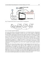
Fig. 2. Experimental set-up to evaluate magneto-optical TE-TM waveguide mode conversion
For the Cd
1-x
Mn
x
Te to be used as a material for the waveguide isolator, several conditions
should be satisfied. For a practical Cd
1-x
Mn
x
Te waveguide isolator, the isolation ratio should
exceed 20 dB, insertion loss should be below 1 dB and operation wavelength range should
be wider than 20 nm. This performance can only be achieved with a magneto-optical
waveguide having a mode conversion ratio above 95 % and a figure-of-merit above 100
deg/dB. Below we will show that using advanced waveguide structure and optimized
fabrication technique, this conditions can be achieved in Cd
1-x
Mn
x
Te waveguide grown on
GaAs substrate.
The Cd
1-x
Mn
x
Te has about 12% lattice mismatch with GaAs. The growth conditions of Cd
1-
x
Mn
x
Te on GaAs substrate should be well optimized. Otherwise, the high density of
dislocation in Cd
1-x
Mn
x
Te film causes high optical loss in Cd
1-x
Mn
x
Te waveguide (Zaets et
al.,1997) and low value of Faraday rotation. The Cd
1-x
Mn
x
Te waveguide was grown by
molecular beam epitaxy (MBE) on GaAs (001) substrate. We optimized the growth
conditions and fabricated the Cd
1-x
Mn
x
Te waveguide in the following way. In the
beginning, GaAs substrate was thermally cleaned at 400
0
C under atomic hydrogen flux to
remove oxides from GaAs surface. Before initiating the growth, the GaAs substrate was kept
for 30 minutes under Zn flux to prevent the formation of the undesired Ga
2
Te
3
compound.
At first, a thin 10 nm ZnTe film was grown on the GaAs substrate to initialize the (001)
growth. Following a 1-µm thick CdTe buffer layer, Cd
1-x
Mn
x
Te waveguide was grown. It
consists of a 3-µm-thick Cd
0.73
Mn
0.27
Te waveguide cladding and a 1-µm-thick Cd
0.77
Mn
0.23
Te
waveguide core. The waveguide core was sandwiched between two 500-nm-thick Cd
1-
x
Mn
x
Te (x=0.27-0.23) graded-refractive-index clad layers, for which the Mn concentration
was changed linearly with thickness. We used the Cd
0.73
Mn
0.27
Te layer as a cladding layer,
since GaAs is an optical absorber with a higher refractive index than that of Cd
1-x
Mn
x
Te, a
single Cd
1-x
Mn
x
Te layer on GaAs does not work as a waveguide. One needs transparent
cladding layers with smaller refractive index. Cd
0.73
Mn
0.27
Te satisfies these conditions
because Cd
1-x
Mn
x
Te with higher Mn concentration has a smaller refractive index and wider
optical band gap. The graded-refractive-index clad layers are essential for Cd
1-x
Mn
x
Te
waveguide to achieve high magneto-optical TE-TM waveguide mode conversion and high
optical isolation.
Figure 2 illustrates the experimental setup for evaluating optical propagation loss and TE-
TM waveguide mode conversion (Zaets & Ando, 2000). A GaP prism was used to couple the
laser light from tunable Ti:sapphire laser (λ=680 -800 nm) into a Cd
1-x
Mn
x
Te waveguide. A
cooled CCD TV-camera collected light scattered normally from the film surface. A linear
polarizer was placed in front of the TV camera with its polarization axis perpendicular to
Frontiers in Guided Wave Optics and Optoelectronics
324
the light propagation direction. With this configuration, only the TE mode component of
waveguiding light can be detected by the high-sensitivity TV camera. In the absence of a
magnetic field, a scattered light streak was seen when the TE mode was excited (Fig. 3(a)),
but it was not seen when TM mode was excited (Fig. 3 (b)). Also, weak dot-like scattering on
defects was seen in both cases.
TM
TE
H=0 H=5 kGauss
H=5 kGaussa)
b)
c)
d)
e)
f)
02468
0
25
50
75
100
Normolazed intensity, %
Propagation distance, mm
0
25
50
75
100
Normolazed intensity, %
TM
TE
H=0 H=5 kGauss
H=5 kGaussa)
b)
c)
d)
e)
f)
02468
0
25
50
75
100
Normolazed intensity, %
Propagation distance, mm
0
25
50
75
100
Normolazed intensity, %
Fig. 3. TM-TE mode conversion ratio in Cd
1-x
Mn
x
Te waveguide at λ=730 nm. (Zayets &
Ando, 2004)
For the evaluation of the magneto-optical TE-TM waveguide mode conversion, a magnetic
field was applied in parallel to the light propagation direction. A light streak with a
periodically modulated intensity was observed for both TE mode excitation (Fig. 3 (c)) and
TM mode excitation (Fig. 3 (d)). Figures 3 (e)-(f) show the measured intensity of the
modulated streak along the propagation length. The intensity was normalized to input
intensity. The oscillations maxima in the case of TE excitation (Fig. 3 (e)) correspond to the
oscillations minima in the case of TM excitation (Fig. 3 (f)) and vice versa. Under an applied
magnetic field the polarization of the waveguide mode rotates because of Faraday effect. If
the TE-TM mode phase mismatch is not zero, the eigenmodes of the waveguide are
elliptically polarized and the rotation between TE and TM polarizations is not complete. As
seen from Figs. 3 (c)- 3 (f), the Cd
1-x
Mn
x
Te waveguide with the graded index cladding layer
shows almost complete mode conversion.
The Cd
1-x
Mn
x
Te waveguide with graded buffer layers has low optical loss, high TE-TM
mode conversion efficiency (more than 98 %) and high isolation ratio (more than 20 dB).
However, high isolation ratio was obtained in narrow about 3 nm wavelength range. For
practical application of the isolator the operation wavelength range should be at least 20 nm.
For the operation of the optical isolator, the rotational angle of Faraday rotator should be 45
0
(Fig.1) for any operational wavelength. Cd
1-x
Mn
x
Te is a diluted magnetic semiconductor. It
has a high value of Faraday rotation, but it is high only near its bandgap and near the
bandgap the dispersion of Faraday rotation is significant as well. Of course, Cd
1-x
Mn
x
Te is a
paramagnetic material and at each wavelength the Faraday rotation can be tuned to 45
0
by
the changing magnetic field. However, such tuning is not practical for real applications
because a practical isolator needs a permanent magnet with a fixed magnetic field. Below
we will show that it is possible to achieve practically dispersion-free Faraday rotation in
Magneto-optical Devices for Optical Integrated Circuits
325
wide wavelength range by combining in a waveguide Cd
1-x
Mn
x
Te bulk material and a
Cd
1-x
Mn
x
Te quantum well (QW).
The Faraday effect in a Cd
1-x
Mn
x
Te QW is greater than that of bulk Cd
1-x
Mn
x
Te and it is not
as dependent on wavelength. However, due to the two-dimensional nature of the QW, its
optical properties become significantly different for light polarized in the plane of the QW
and perpendicular to the QW. Therefore, for a waveguide composed of only a single QW,
there is a big difference between propagation constants of TE and TM modes. Due to TE-TM
mode phase mismatch, the linearly polarized light can be easily converted to elliptically
polarized light, which reduces the performance of the isolator. Therefore, a waveguide
composed of only a single QW cannot be used for the isolator application.
In order to make a high performance isolator, we need a large, wavelength independent
Faraday effect and small phase mismatch between TE and TM modes. For that purpose, we
proposed using an optical waveguide that combines Cd
1-x
Mn
x
Te bulk material and a single
QW (Debnath et.al. 2004)
Figure 4 shows the (Cd,Mn)Te/(Cd,Zn)Te QW waveguide structure. There are two buffer
layers of ZnTe (10 nm) and CdTe (1 µm) and a Cd
0.71
Mn
0.29
Te (3 µm) waveguide clad layer.
The waveguide core layer was sandwiched between two Cd
1-x
Mn
x
Te (0.5 µm) graded layers
in order to reduce TE-TM mode phase mismatch. The waveguide core consists of a Cd
0.76
Mn
0.2
Te/Cd
0.75
Zn
0.25
Te single QW and a 1-µm-thick Cd
0.75
Mn
0.25
Te layer, where thickness
of the Cd
0.76
Mn
0.24
Te well varies between 20–100 Å and the thickness of Cd
0.75
Zn
0.25
Te
barrier is 100 Å.
Substrate: GaAs (001)
Buffer: ZnTe (10 nm)
Buffer: CdTe (1 μ m)
Clad: Cd
0.71
Mn
0.29
Te (3 μ m)
Barrier: Cd
0.75
Zn
0.25
Te (100? )
Graded: Cd
1-x
Mn
x
Te (x=0.29-0.25)
Well: Cd
0.76
Mn
0.24
Te (20? -100? )
Barrier: Cd
0.75
Zn
0.25
Te (100? )
Cd
0.75
Mn
0.25
Te (1 μ m)
Graded: Cd
1-x
Mn
x
Te (x=0.25-0.29)
Core
Fig. 4. Structure of a (Cd,Mn)Te waveguide with (Cd,Mn)Te/(Cd,Zn)Te QW. The
waveguiding light intensity distribution is shown in the right side . (Debnath et al, 2007)
Figure 5 shows a spatially modulated light streak of the waveguide mode at two different
wavelengths (760 and 785 nm) for the waveguides with QW and without QW. The high
contrast between the minima and maxima of the light intensity oscillations shows that
complete mode conversion is attained for both waveguides. The distance between peaks
corresponds to 180 degrees of the rotation. For the waveguide without QW [Figs. 5 (c) and 5
(d)], there is a big difference of the rotational period for these two wavelengths. However,
for the waveguide with QW [Figs. 5(a) and 5 (b)], there was no such difference. This means
that, for the waveguide with QW, the Faraday rotation at these two wavelengths is the
same. Also, for the waveguide with QW, the oscillation period is much shorter than that of
Frontiers in Guided Wave Optics and Optoelectronics
326
the waveguide without QW. This corresponds to the larger Faraday rotation in the
waveguide with QW.
(a)
λ = 710 nm
λ=785 nmλ=760 nm
(b)
H=5.5
kG
H=5.5
kG
2
mm
with
QW
(c) (d)
without
QW
2
mm
λ=760 nm λ=785 nm
H=5.5
kG
H=5.5
kG
(a)
λ = 710 nm
λ=785 nmλ=760 nm
(b)
H=5.5
kG
H=5.5
kG
2
mm
with
QW
(c) (d)
without
QW
2
mm
λ=760 nm λ=785 nm
H=5.5
kG
H=5.5
kG
Fig. 5. Spatially modulated light streak from waveguide TE mode for CdMnTe waveguide
with QW (a), (b) and waveguide without QW (c), (d) at λ = 760 nm (a), (c) and λ = 785 nm
(b), (d) under magnetic field of 5.5 kG . (Debnath et al, 2007)
Figure 6 compares the Faraday effect in Cd
1-x
Mn
x
Te waveguide with QW and without QW
at H=5.5 kG. In the case of the waveguide with QW, the Faraday rotation is very high (~1800
deg/cm) and it is almost constant in a wide wavelength range. Figure 7 shows the
wavelength range within which more than 95% conversion efficiency was obtained for the
waveguide with single QW as a function of well width. For well widths of 20–40 Å, the
operational wavelength range is as wide as 25-nm. However, for thicker well widths of 70–
100 Å, the operational wavelength range sharply decreases. Analysis shows that the
expansion of the wavelength range for thinner QW waveguides was due to the reduction of
the mode phase mismatch, to as low as 50 deg/cm, whereas this value rose to more than 500
deg/cm for thicker QW waveguides. Thinner QW waveguides have high Faraday rotation
(≈ 2000 deg/cm) and small phase mismatch (≈ 50 deg/cm) This is the reason why thinner
QW waveguides provided a wider operational wavelength range of complete mode
conversion. From this result we conclude that, for the practical optical isolator application,
only waveguides with a single QW thinner than 40 Å can be used.
740 750 760 770 780 790
0
500
1000
1500
2000
2500
H = 5.5 kG
Wavelength λ (nm)
Faraday rotation Θ
F
(deg/cm)
with QW
without QW
Fig. 6. Faraday rotation in Cd
1-x
Mn
x
Te waveguide with QW and without QW . (Debnath et
al, 2007)
Magneto-optical Devices for Optical Integrated Circuits
327
0 25 50 75 100
0
5
10
15
20
25
30
mode conversion: 100%
Well width (Å)
Wavelength range (nm)
of isolation ratio
Quantum well width (Å)
Wavelength range (nm) of
complete mode conversion
0 25 50 75 100
0
10
20
30
isolation: 27 dB
Fig. 7. Wavelength range, within which the complete mode conversion is obtained, as a
function of QW width. Inset shows the isolation ratio. (Debnath et al, 2004)
For an integrated optical isolator, the CdMnTe magneto-optical waveguide has to be
integrated with a reciprocal polarization rotator and a polarizing beam splitter. Both these
components can be fabricated utilizing passive optical waveguides. The material of the
waveguides is not essential for the operation of these components. Therefore, it is better to
use the same passive waveguides as utilized for optical interconnection in a photonic circuit,
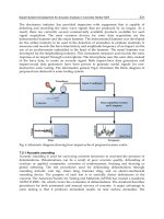
where the isolator should be integrated. Figure 8 shows an example of a waveguide-type
reciprocal polarization rotator. It is a passive optical waveguide in which the top is cut at an
angle of 45 degrees. TM and TE modes are not eigenmodes in this waveguide. Therefore,
there is a conversion between TM and TE mode along mode propagation. The length of this
waveguide can be adjusted to achieve the desirable angle of polarization rotation. The
waveguide type reciprocal polarization rotators were demonstrated utilizing Si waveguide
(Brooks et al., 2006], AlGaAs waveguides (Huang et al., 2000) and GaInAsP/InP
waveguides (Kim et al., 2009). Figure 11 shows an example of a waveguide-type polarizing
beam splitter. It is a 2x2 waveguide splitter. In any waveguide splitter, the coupling
efficiency between an input ports and an output ports depends on the value of mode
propagation constant. Generally, in an optical waveguide the propagation constants of TM
and TE modes are different. Therefore, it is possible to adjust the splitter so that the TM
mode couples from port 1 into port 4 and the TE mode couples from port 1 into port 3. The
waveguide-type polarizing beam splitters were demonstrated utilizing Si waveguide
(Fukuda et al., 2006) and InGaAsP–InP waveguides (Augustin et al., 2007).
reciprocal
rotator
Fig. 8. Waveguide-type reciprocal polarization rotator.
Frontiers in Guided Wave Optics and Optoelectronics
328
T
M
1
port 1
port 2
port 4
port 3
T
M
2
T
M
2
T
E
2
T
E
1
T
M
1
T
E
1
T
E
2
Fig. 9. Waveguide-type polarization beam splitter.
Figure 10 shows the design of a waveguide-type polarization-independent optical isolator. It
consists of two polarizing beam splitters connected by two arms. Each arm consists of an 45-
degree reciprocal rotator and a 45-degree Cd
1-x
Mn
x
Te -made Faraday rotator. There is an
optical absorber at port 2 to absorb backward travelling light. In the forward direction, the
direction of polarization rotation in the Faraday rotator is the same as that in the reciprocal
rotator and the total rotation angle by the reciprocal rotator and the Faraday rotator is 90
degrees. The light of both polarizations propagates through the isolator from input 1 port to
output port 3. In the backward direction, the direction of polarization rotation in the
Faraday rotator is opposite to that in the reciprocal rotator due to the non-reciprocal nature
of the Faraday rotator. In this case, the total rotation angle is zero. The light propagates from
output port 3 to the port 2, where there is an absorber. Therefore, the input port 1 is
isolated. The optical paths for each polarization are shown in Fig. 10. A waveguide-type
polarization-independent optical circulator can be fabricated utilizing the same design. In
this case the correspondence between the input and output ports is: port 1-> port 3, port 2 –
>port 4, port 3 -> port 2, port 4 -> port 1.
T
M
T
E
T
M
T
M
T
M
T
M
T
E
T
E
T
E
T
M
T
E
T
E
T
M
T
E
T
M
T
E
45 degree
CdMnTe
Faraday
rotator
input
absorber
output
port 3
port 4
port 1
port 2
45 degree
reciprocal
rotator
Fig. 10. Polarization-independent waveguide-type optical isolator / circulator. Polarization
transformations for both propagation directions are shown.
In conclusion, the high performance of Cd
1-x
Mn
x
Te waveguide isolator grown on GaAs
substrate was demonstrated. Complete TE-TM mode conversion, a high Faraday rotation of
2000 deg/cm, a high isolation ratio of 27 dB, a low optical loss of 0.5 dB/cm, and a high
magneto-optical figure-of-merit of 2000 deg/dB/kG were achieved in a wide 25-nm
wavelength range. These values are comparable or better to that of commercial discrete
isolators. The propagation of waveguide mode in Cd
1-x
Mn
x
Te waveguide is very similar to
the light propagation in magneto-optical bulk media. Therefore, non-reciprocal elements
such as an optical isolator, circulator and polarization independent isolator can be fabricated
by Cd
1-x
Mn
x
Te waveguides using a similar scheme as is used for free space components.
Therefore, using Cd
1-x
Mn
x
Te all these components can be integrated with semiconductors
optoelectronical components.
Magneto-optical Devices for Optical Integrated Circuits
329
3. Ferromagnetic metal/semiconductor hybrid isolator
Both types of isolators, either made of Cd
1-x
Mn
x
Te or made of garnets, required high-crystal
quality materials in order to have a low optical loss and a high value of Faraday rotation. In
the case of Cd
1-x
Mn
x
Te, the magneto-optical film can be directly grown on a semiconductor
substrate. The defect density in Cd
1-x
Mn
x
Te film should be kept low until the end of the
microfabrication process. For the fabrication of integrated optical circuits it is more
convenient to use common fabrication technique like sputtering, e-beam evaporation and
lift-off. Ferromagnetic metals, like Fe, Co or Ni are very attractive for this purpose. They
have high magneto-optical constants and the microfabrication of these metals is simple and
well established for optoelectronic integrated circuits. For example, Cr and Co is often used
as a metal for Ohmic contact to p-GaAs and p-InGaAs.
We predicted theoretically (Zaets & Ando, 1999) and proved experimentally (Zaets & Ando,
2005) the effect of non-reciprocal loss in hybrid semiconductor/ferromagnetic metal
waveguides. This effect can be use for a new design of waveguide optical isolator. For this
design, the magnetization of the ferromagnetic metal was perpendicular to the light
propagation direction and lay in the film plane (Voigt configuration). In this case a large
difference exists in values of loss/gain for TM modes propagating in opposite directions.
Thus, an amplifier covered by a ferromagnetic metal can itself function as an optical isolator.
This ferromagnetic-metal/ semiconductor hybrid isolator can be beneficial for monolithic
integration of the optical isolator with semiconductor optoelectronic devices, because its
structure is very similar to the structure of a laser diode and its fabrication process is almost
the same as that of a laser diode. Therefore, the isolator can be integrated utilizing the
present technology for a semiconductor laser diode and a semiconductor amplifier.
The effect of the non-reciprocal loss is unique for the hybrid waveguides. In the case of the
light propagation in a bulk MO material the non-reciprocal effect (variation of optical
properties for opposite directions of light propagation) occurs only when the magnetization
of the material is parallel to the light propagation (Faraday effect and magnetic circular
dichroism). There is no non-reciprocal effect, if the light propagates perpendicularly to the
magnetization. On the contrary, in a MO waveguide, even if the magnetization is
perpendicular to the light propagation direction and lies in the film plane, the TM mode has
a non-reciprocal change of the propagation constant.
Figure 11 compares the magneto-optical effect in a bulk material and in an optical
waveguide covered by ferromagnetic metal. In the bulk material, when the light propagates
along magnetic field, there are two magneto-optical effects: magnetic circular dichroism
(MCD) and Faraday effect. In magnetic materials the spin-up and spin-down bands are split
along the magnetic field. Due to the conservation law of the time inverse symmetry, the
light of the left circular polarization interacts only with the spin-up band and the light of the
right circular polarization interacts only with the spin-down band. (In general, the light of
elliptical polarization interacts solely with one spin band). Therefore, there is a difference of
refractive index (Faraday effect) and of absorption (MCD effect) for the left and right
circular polarizations, when the light propagates along the magnetic field. When the
magnetic field is perpendicular to the light propagation, there is no linear magneto-optical
effect. The case of a waveguide covered by magnetic metal is different. Inside of the metal
the optical field is evanescent. As it will be shown below, in the case of evanescent field, the
polarization rotates in xz-plane perpendicularly to the waveguide mode propagation
direction (Fig. 11) even without magnetic field or anisotropy. Therefore, if the magnetic field