Semiconductor Technologies Part 8 doc
Bạn đang xem bản rút gọn của tài liệu. Xem và tải ngay bản đầy đủ của tài liệu tại đây (3.82 MB, 30 trang )
GaN-basedmetal-oxide-semiconductordevices 203
Matsumura, H. (1986). Catalytic chemical vapor deposition (CTL-CVD) method producing
high quality hydrogenated amorphous silicon. Jpn. J. Appl. Phys., Vol. 25, No. 12,
(Nov. 1986) (L949-L951), 0021-4922
Medjdoub, F.; Sarazin, N.; Tordjman, M.; Magis, M.; di Forte-Poisson, M. A.; Knez, M.;
Delos, E.; Gaquiére, C.; Delage, S. L. & Kohn, E. (2007). Characteristics of
Al
2
O
3
/AlInN/GaN MOSHEMT. Electron. Lett., Vol. 43, No. 12, (Jun. 2007) (691-692),
0013-5194
Mehandru, R.; Gila, B. P.; Kim, J.; Johnson, J. W.; Lee, K. P.; Luo, B.; Onstine, A. H.;
Abernathy, C. R.; Pearton, S. J. & Ren, F. (2002). Electrical characterization of GaN
metal oxide semiconductor diode using Sc
2
O
3
as the gate oxide. Electrochem. Solid
State Lett., Vol. 5, No. 7, (Apr. 2002) (G51-G53), 1099-0062
Mehandru, R.; Luo, B.; Kim, J.; Ren, F.; Gila, B. P.; Onstine, A. H.; Abernathy, C. R.; Pearton,
S. J.; Gotthold, D.; Birkhahn, R.; Peres, B.; Fitch, R.; Gillespie, J.; Jenkins, T.; Sewell,
J.; Via, D. & Crespo, A. (2003). AlGaN/GaN metal-oxide-semiconductor high
electron mobility transistors using Sc
2
O
3
as the gate oxide and surface passivation.
Appl. Phys. Lett., Vol. 82, No. 15, (Apr. 2003) (2530-2532), 0003-6951
Meneghesso, G.; Verzellesi, G.; Pierobon, R.; Rampazzo, F.; Chini, A.; Mishra, U. K.; Canali,
C. & Zanoni, E. (2004). Surface-related drain current dispersion effects in AlGaN-
GaN HEMTs, IEEE Trans. Electron Devices, Vol. 51, No. 10, (Oct. 2003) (1554 - 1561),
0018-9383
Misstele, D.; Rotter, T.; Horn, A.; Katz, O.; Bougrioua, Z.; Aderhold, J.; Graul, J.; Bahir, G. &
Salzman, J. (2003). Incorporation of dielectric layers into the processing of III-
nitride-based heterostructure field-effect transistors. J. Electron. Mater., Vol. 32, No.
5, (May 2003) (355-363), 0361-5235
Mittereder, J. A.; Binari, S. C.; Klein, P. B.; Roussos, J. A.; Katzer, D. S.; Storm, D. F.; Koleske,
D. D.; Wickenden, A. E. & Henry, R. L. (2003). Current collapse induced in
AlGaN/GaN high-electron-mobility transistors by bias stress. Appl. Phys. Lett., Vol.
83, No. 8, (Aug. 2003) (1650-1652), 0003-6951
Mizutani, T.; Ohno, Y.; Akita, M.; Kishimoto, S.; & Maezawa, K. (2003). A study on current
collapse in AlGaN/GaN HEMTs induced by bias stress. IEEE Trans. Electron
Devices, Vol. 5 , No. 10, (Oct. 2003) (2015-2020), 0018-9383
Morkoc, H.; Strite, S.; Gao, G. B.; Lin, M. E.; Sverdlov, B. & Burns, M. (1994). Large-band-gap
SiC, III-V nitride, and II-VI ZnSe-based semiconductor device technologies. J. Appl.
Phys., Vol. 76, No. 3, (Aug. 1994) (1363-1398), 0021-8979
Neaman, D. A. (1997). Semiconductor physics and devices: basic principles, Irwin, 025608405X,
Homewood IL
Nakamura, S.; Senoh, M.; Nagahama, S.; Iwasa, N.; Yamada, T.; Matsushita, T.; Kiyoku, H.;
& Sugimoto, Y. (1996). InGaN-based multi-quantum-well-structure laser diodes.
Jpn. J. Appl. Phys. Lett., Vol. 35, No. 1B, (L74-L76) (Jan. 1996). 0021-4922
Nakamura, S.; Senoh, M.; Nagahama, S. I.; Iwasa, N.; & Yamada, T. (1996). Characteristics of
InGaN multi-quantum-well-structure laser diodes, Appl. Phys. Lett., Vol. 68, No.3,
(Mar. 1996) (3269-3271), 0003-6951
Nakamura, S.; Senoh, M.; Nagahama, S.; Iwasa, N.; Yamada, T.; Sushita, T. M.; Kiyoku, H.;
Sugimoto, Y.; Kozaki, T.; Umemoto, H.; Sano, M.; & Chocho, K. (1998).
InGaN/GaN/AlGaN-based laser diodes with modula-tion-doped strained-layer
superlattices grown on an epitaxially laterally overgrown gan substrate. Appl. Phys.
Lett., Vol. 72, No. 12, (Nov. 1998) (211-213), 0003-6951
Nakano, Y. & Kachi, T. (2003). Characteristics of SiO
2
/n-GaN interfaces with β-Ga
2
O
3
interlayers. Appl. Phys. Lett., Vol. 83, No. 21, (Nov. 2003) (4336-4338), 0003-6951
Navarro, A.; Rivera, C.; Pereiro, J.; Muñoz, E.; Imer, B.; DenBaars, S. P.; & Speck, J. S. (2009).
High responsivity a-plane GaN-based metal-semiconductor-metal photodetectors
for polarization-sensitive applications. Appl. Phys. Lett., Vol. 94, (May 2009) (213512-
213514), 0003-6951
Ohno, Y. & Kuzuhara, M. (2001). Applications of GaN-based heterojunction fets for
advanced wireless communication. IEEE Trans. Electron Deices, Vol. 48, No. 3, (Mar.
2001) (517-523), 0018-9383
Okita, H.; Kaifu, K.; Mita, J.; Yamada, T.; Sano, Y.; Ishikawa, H.; Egawa, T. & Jimbo, T.
(2003). High transconductance AlGaN/GaN-HEMT with recessed gate on sapphire
substrate. Phys. Stat. Sol. (a), Vol. 200, No. 1, (Nov. 2003) (187-190), 0031-8965
Onojima, N.; Higashiwaki, M.; Suda, J.; Kimoto, T.; Mimura, T. & Mastsui, T. (2007).
Reduction in potential barrier height of AlGaN/GaN heterostructures by SiN
passivation. J. Appl. Phys., Vol. 101, No. 4, (Feb. 2007) (043703-1-043703-6), 0021-
8979
Palacios, T.; Chakraborty, A.; Heikman, S.; Keller, S.; DenBaars, S. P. & Mishra, U. K. (2006).
AlGaN/GaN high electron mobility transistors with InGaN back-barriers. IEEE
Electron Device Lett., Vol. 27, No. 1, (Jan. 2006) (13-15), 0741-3106
Park, K. Y.; Cho, H. I.; Choi, H. C.; Bae, Y. H.; Lee, C. S.; Lee, J. L. & Lee, J. H. (2004). Device
characteristics of AlGaN/GaN MIS-HFET using Al
2
O
3
-HfO
2
laminated high-k
dielectric. Jpn.J. Appl. Phys., Vol. 43, No. 11A, (Oct. 2004) (L1433-L1435), 0021-4922
Pau, J. L.; Rivera, C.; MuĖoz, E.; Calleja, E.; Schühle, U.; Frayssinet, E.; Beaumont, B.; Faurie,
J. P.; & Gibart, P. (2004). Response of ultra-low dislocation density gan
photodetectors in the near- and vacuum-ultraviolet. J. Appl. Phys., Vol. 95, No. 12,
(June 2004) (8275-8279), 0021-8979
Peng, P. C.; Peng, W. R.; Feng, K. M.; Chiou, H. Y.; Chen, J.; Kuo, H. C.; Wang, S. C. & Chi, S.
(2006). OCDMA light source using directly modulated Fabry–Pérot laser diode in
an external injection scheme. IEEE Photon. Technol. Lett., Vol. 18, No. 9, (May 2006)
(1103-1105), 1041-1135
Peransin, J. M.; Vignaud, P.; Rigaud, D. & Vandamme, L. K. J. (1990). 1/f noise in MODFETs
at low drain bias. IEEE Trans. Electron Deices, Vol. 37, No. 10, (Oct. 1990) (2250-
2253), 0018-9383
Poate , J. M.; Tu, K. N. & Mayer, J. W. (1978). Thin films, inter-diffusion and reactions, Wiley,
0471022381, New York
Pozzovivo, G.; Kuzmik, J.; Golka, S.; Schrenk, W.; Strasser, G.; Pogany, D.; Čičo, K.; Ťapajna,
M.; Fröhlich, K.; Carlin, J. F.; Gonschorek, M.; Feltin, E. & Grandjean, N. (2007).
Gate insulation and drain current saturation mechanism in InAlN/GaN metal-
oxide-semiconductor high-electron-mobility transistors. Appl. Phys. Lett., Vol. 91,
No. 4, (Jul. 2007) (043509-1-043509-3), 0003-6951
SemiconductorTechnologies204
Rai, S.; Adivarahan, V.; Tipirneni, N.; Koudymov, A.; Yang, J.; Simin, G. & Khan, M. A.
(2006). Low threshold-14W/mm ZrO
2
/AlGaN/GaN metal-oxide-semiconductor
heterostructure field effect transistors. Jpn. J. Appl. Phys., Vol. 45, No. 6A, (Jun. 2006)
(4985-4987), 0021-4922
Reimbold, G. (1984). Modified 1/f trapping noise theory and experiments in MOS
transistors biased from weak to strong inversion-influence of interface states. IEEE
Trans. Electron Deices, Vol. 31, No. 9, (Sep. 1984) (1190-1198), 0018-9383
Ren, F.; Abernathy, C. R.; Mackenzie, J. D.; Gila, B. P.; Pearton, S. J.; Hong, M.; Marcus, M.
A.; Schurman, M. J.; Baca, A. G. & Shul, R. J. (1998). Demonstration of GaN MIS
diodes by using AlN and Ga
2
O
3
(Gd
2
O
3
) as dielectrics. Solid-State Electron., Vol. 42,
No. 12, (Dec. 1998) (2177-2181), 0038-1101
Ren, F.; Pearton, S. J.; Abernathy, C. R.; Baca, A.; Cheng, P.; Shul, R. J.; Chu, S. N. G.; Hong,
M.; Schurman, M. J. & Lothian, J. R. (1999). GaN metal oxide semiconductor field
effect transistors. Solid-State Electron., Vol. 43, No. 9. (Sep. 1999) (1817-1820), 0038-
1101
Rotter, T.; Mistele, D.; Stemmer, J.; Fedler, F.; Aderhold, J. & Graul, J. (2000). Photoinduced
oxide film formation on n-type GaN surfaces using alkaline solution. Appl. Phys.
Lett., Vol. 76, No. 26, (Jun. 2000) (3923-3925), 0003-6951
Rossetti, M.; Smeeton, T. M.; Tan, W. S.; Kauer, M.; Hooper, S. E.; Heffernan, J.; Xiu, H. &
Humphreys, C. J. (2008). Degradation of InGaN/GaN Laser diodes analyzed by
microphotoluminescence and microelectroluminescence Mappings. Appl. Phys.
Lett., Vol. 92, No. 15, (Apr. 2008) (151110-1- 151110-3), 0003-6951
Rumyantsev, S. L.; Pala, N.; Shur, M. S.; Gaska, R.; Levinshtein, M. E.; Khan, M. A.; Simin,
G.; Hu, X. & Yang, J. (2000). Effect of gate leakage current on noise properties of
AlGaN/GaN field effect transistors. J. Appl. Phys., Vol. 88, No. 11, (Dec. 2000) (6726-
6730), 0021-8979
Rumyantsev, S. L.; Pala, N.; Shur, M. S.; Gaska, R.; & Levinshtein, M. E. (2001). Low-
frequency noise in Al
0.4
Ga
0.6
N-based schottky barrier photodetectors, Appl. Phys.
Lett., Vol. 79, No. 6, (May 2001) (866-868), 0003-6951
Sacconi, F.; Carlo, A. D.; Lugli, P. & Morkoc, H. (2001). Spontaneous and piezoelectric
polarization effects on the output characteristics of AlGaN/GaN heterojunction
modulation doped FETs. IEEE Trans. Electron Deices, Vol. 48, No. 3, (Mar. 2001)
(450-457), 0018-9383
Saitoh, T.; Kumagai, M.; Wang, H.; Tawara, T.; Nishida, T.; Akasaka, T.; & Kobayashi, N.
(2003). Highly reective distributed bragg reectors using a deeply etched
semiconductor/air grating for InGaN/GaN laser diodes. Appl. Phys. Lett., Vol.82,
No. 23, (Jun. 2003) (4426-4429). 0003-6951
Saripalli, Y. N.; Pei, L.; Biggerstaff,T.; Ramachandran, S.; Duscher, G. J.; Johnson, M. A. L.;
Zeng, C.; Dandu, K.; Jin, Y. & D. Barlag, W. (2007), Transmission electron
microscopy studies of regrown GaN ohmic contacts on patterned substrates for
metal oxide semiconductor field effect transistor applications, Appl. Phys. Lett., Vol.
90, No. 20, (May 2007) (204106-1-204106-3), 0003-6951
Schoedl, T.; Schwarza, U. T.; Kümmler, V.; Furitsch, M.; Leber, A.; Miler, A.; Lell, A. &
Härle, V. (2005). Facet degradation of GaN heterostructure laser diodes. J. Appl.
Phys., Vol. 97, No. 12, (Jun. 2005) (123102-1-123102-8), 0021-8979
Schroder, D. K. (1998). Semiconductor material and device characterization, Wiley, 0471241393,
New York
Seo, S.; Lee, K. K.; Kang, Sangbeom; Huang, S.; Doolittle, W. A.; Jokerst, N. M.; Brown, A. S.
& Brooke, M. A. (2002). The heterogenous integration of GaN thin-film metal-
semiconductor-metal photodetectors onto silicon. IEEE Photon. Technol. Lett., Vol.
14, No. 2, (Feb. 2002) (185-187), 1041-1135
Shen, C. F.; Chang, S. J.; Ko, T. K.; Kuo, C. T.; Shei, S. C.; Chen, W. S.; Lee, C. T.; Chang C. S.,;
& Chiou, Y. Z. (2006). Nitride-based light emitting diodes with textured sidewalls
and pillar waveguides, IEEE Photon. Technol. Lett., Vol 18, No. 23, (Dec. 2006) (2517-
2519), 1041-1135
Shih, C. F.; Li, W. M.; Shu, S. C.; Hsiao, C. Y. & Hung, K. T. (2009). Electrical Properties of
Al/HfO
2
/n-GaN Prepared by Reactive Sputtering Method. Jpn.J. Appl. Phys., Vol.
48, No. 2, (Feb. 2009) (020224-1-020224-3), 0021-4922
Shih, C. F.; Hung, K. T.; Hsiao, C. Y.; Shu, S. C. & Li, W. M. (2009). Investigations of GaN
Metal-oxide-semiconductor Capacitors With Sputtered HfO
2
Gate Dielectrics. J.
Alloy. Compd, Vol. 480, No. 2, (Jul. 2009) (541-546), 0925-8388
Seo, H. C.; Chapman, P.; Cho, H. I.; Lee, J. H. & Kim, K. (2008). Ti-based nonalloyed ohmic
contacts for Al
0.15
Ga
0.85
N/GaN high electron mobility transistors using regrown n
+
-
GaN by plasma assisted molecular beam epitaxy, Appl. Phys. Lett., Vol 93, No. 10,
(Sept. 2008) (102102-1-102102-3), 0003-6961
Sheu, J. K.; Lee, M. L.; Yeh, L. S.; Kao, C. J.; Tun, C. J.; Chen, M. G.; Chi, G. C.; Chang, S. J.;
Su, Y. K. & Lee, C. T. (2002). Planar GaN n
-p photodetectors formed by Si
implantation into p-GaN. Appl. Phys. Lett., Vol. 81, No. 22, (Dec. 2006) (4263-4265),
0003-6951
Simin, G.; Koudymou, A.; Fatima, H.; Zhang, J.; Yang, J.; Khan, M. A.; Hu, X.; Tarakji, A.;
Gaska, R. & Shur, M. S. (2002). SiO
2
/AlGaN/InGaN/GaN MOSDHFETs. IEEE
Electron Device Lett., Vol. 23, No. 8, (Aug. 2002) (458-460), 0741-3106
Simin, G.; Adivarahan, V.; Yang, J.; Koudymov, A.; Rai, S. & Khan, M. A. (2005). Stable
20W/mm AlGaN-GaN MOSHFET. Electron. Lett., Vol. 41, No. 13, (Jun. 2005) (774-
775), 0013-5194
Smorchkova, I. P.; Elsass, C. R.; Ibbetson, J. P.; Vetury, R.; Heying, B.; Fini, P.; Haus, E.;
DenBaars, S. P.; Speck, J. S. & Mishra, U. K. (1999). Polarization-induced charge and
electron mobility in AlGaN/GaN heterostructures grown by plasma-assisted
molecular-beam epitaxy. J. Appl. Phys., Vol. 86, No. 8, (Oct. 1999) (4520-4526), 0021-
8979
Su, Y. K.; Chang, P. C.; Chen, C. H.; Chang, S. J.; Yu, C. L.; Lee, C. T.; Lee, H. Y.; Gong, J.;
Chen, P. C.; & Wang, C. H. (2005). Nitride-based MSM UV photodetectors with
photo-chemical annealing schottky contacts. Solid-State Electron., Vol. 49, No. 3,
(Mar. 2005) (459-463), 0038-1101
Suski, T.; Franssen, G.; Perlin, P.; Bohdan, R.; Bercha, A.; Adamiec, P.; Dybala, F.;
Trzeciakowski, W.; Prystawko, P.; Leszczyński, M.; Grzegory, I.; & Porowski, S.
(2004). A pressure-tuned blue-violet InGaN/GaN laser diode grown on bulk gan
crystal. Appl. Phys. Lett., Vol. 62, No. 23, (Feb. 2004) (1236-1238), 0003-6951
Sze, S. M. (2002). Semiconductor Devices-Physics & Technology, Wiley, 0471333727, New York
GaN-basedmetal-oxide-semiconductordevices 205
Rai, S.; Adivarahan, V.; Tipirneni, N.; Koudymov, A.; Yang, J.; Simin, G. & Khan, M. A.
(2006). Low threshold-14W/mm ZrO
2
/AlGaN/GaN metal-oxide-semiconductor
heterostructure field effect transistors. Jpn. J. Appl. Phys., Vol. 45, No. 6A, (Jun. 2006)
(4985-4987), 0021-4922
Reimbold, G. (1984). Modified 1/f trapping noise theory and experiments in MOS
transistors biased from weak to strong inversion-influence of interface states. IEEE
Trans. Electron Deices, Vol. 31, No. 9, (Sep. 1984) (1190-1198), 0018-9383
Ren, F.; Abernathy, C. R.; Mackenzie, J. D.; Gila, B. P.; Pearton, S. J.; Hong, M.; Marcus, M.
A.; Schurman, M. J.; Baca, A. G. & Shul, R. J. (1998). Demonstration of GaN MIS
diodes by using AlN and Ga
2
O
3
(Gd
2
O
3
) as dielectrics. Solid-State Electron., Vol. 42,
No. 12, (Dec. 1998) (2177-2181), 0038-1101
Ren, F.; Pearton, S. J.; Abernathy, C. R.; Baca, A.; Cheng, P.; Shul, R. J.; Chu, S. N. G.; Hong,
M.; Schurman, M. J. & Lothian, J. R. (1999). GaN metal oxide semiconductor field
effect transistors. Solid-State Electron., Vol. 43, No. 9. (Sep. 1999) (1817-1820), 0038-
1101
Rotter, T.; Mistele, D.; Stemmer, J.; Fedler, F.; Aderhold, J. & Graul, J. (2000). Photoinduced
oxide film formation on n-type GaN surfaces using alkaline solution. Appl. Phys.
Lett., Vol. 76, No. 26, (Jun. 2000) (3923-3925), 0003-6951
Rossetti, M.; Smeeton, T. M.; Tan, W. S.; Kauer, M.; Hooper, S. E.; Heffernan, J.; Xiu, H. &
Humphreys, C. J. (2008). Degradation of InGaN/GaN Laser diodes analyzed by
microphotoluminescence and microelectroluminescence Mappings. Appl. Phys.
Lett., Vol. 92, No. 15, (Apr. 2008) (151110-1- 151110-3), 0003-6951
Rumyantsev, S. L.; Pala, N.; Shur, M. S.; Gaska, R.; Levinshtein, M. E.; Khan, M. A.; Simin,
G.; Hu, X. & Yang, J. (2000). Effect of gate leakage current on noise properties of
AlGaN/GaN field effect transistors. J. Appl. Phys., Vol. 88, No. 11, (Dec. 2000) (6726-
6730), 0021-8979
Rumyantsev, S. L.; Pala, N.; Shur, M. S.; Gaska, R.; & Levinshtein, M. E. (2001). Low-
frequency noise in Al
0.4
Ga
0.6
N-based schottky barrier photodetectors, Appl. Phys.
Lett., Vol. 79, No. 6, (May 2001) (866-868), 0003-6951
Sacconi, F.; Carlo, A. D.; Lugli, P. & Morkoc, H. (2001). Spontaneous and piezoelectric
polarization effects on the output characteristics of AlGaN/GaN heterojunction
modulation doped FETs. IEEE Trans. Electron Deices, Vol. 48, No. 3, (Mar. 2001)
(450-457), 0018-9383
Saitoh, T.; Kumagai, M.; Wang, H.; Tawara, T.; Nishida, T.; Akasaka, T.; & Kobayashi, N.
(2003). Highly reective distributed bragg reectors using a deeply etched
semiconductor/air grating for InGaN/GaN laser diodes. Appl. Phys. Lett., Vol.82,
No. 23, (Jun. 2003) (4426-4429). 0003-6951
Saripalli, Y. N.; Pei, L.; Biggerstaff,T.; Ramachandran, S.; Duscher, G. J.; Johnson, M. A. L.;
Zeng, C.; Dandu, K.; Jin, Y. & D. Barlag, W. (2007), Transmission electron
microscopy studies of regrown GaN ohmic contacts on patterned substrates for
metal oxide semiconductor field effect transistor applications, Appl. Phys. Lett., Vol.
90, No. 20, (May 2007) (204106-1-204106-3), 0003-6951
Schoedl, T.; Schwarza, U. T.; Kümmler, V.; Furitsch, M.; Leber, A.; Miler, A.; Lell, A. &
Härle, V. (2005). Facet degradation of GaN heterostructure laser diodes. J. Appl.
Phys., Vol. 97, No. 12, (Jun. 2005) (123102-1-123102-8), 0021-8979
Schroder, D. K. (1998). Semiconductor material and device characterization, Wiley, 0471241393,
New York
Seo, S.; Lee, K. K.; Kang, Sangbeom; Huang, S.; Doolittle, W. A.; Jokerst, N. M.; Brown, A. S.
& Brooke, M. A. (2002). The heterogenous integration of GaN thin-film metal-
semiconductor-metal photodetectors onto silicon. IEEE Photon. Technol. Lett., Vol.
14, No. 2, (Feb. 2002) (185-187), 1041-1135
Shen, C. F.; Chang, S. J.; Ko, T. K.; Kuo, C. T.; Shei, S. C.; Chen, W. S.; Lee, C. T.; Chang C. S.,;
& Chiou, Y. Z. (2006). Nitride-based light emitting diodes with textured sidewalls
and pillar waveguides, IEEE Photon. Technol. Lett., Vol 18, No. 23, (Dec. 2006) (2517-
2519), 1041-1135
Shih, C. F.; Li, W. M.; Shu, S. C.; Hsiao, C. Y. & Hung, K. T. (2009). Electrical Properties of
Al/HfO
2
/n-GaN Prepared by Reactive Sputtering Method. Jpn.J. Appl. Phys., Vol.
48, No. 2, (Feb. 2009) (020224-1-020224-3), 0021-4922
Shih, C. F.; Hung, K. T.; Hsiao, C. Y.; Shu, S. C. & Li, W. M. (2009). Investigations of GaN
Metal-oxide-semiconductor Capacitors With Sputtered HfO
2
Gate Dielectrics. J.
Alloy. Compd, Vol. 480, No. 2, (Jul. 2009) (541-546), 0925-8388
Seo, H. C.; Chapman, P.; Cho, H. I.; Lee, J. H. & Kim, K. (2008). Ti-based nonalloyed ohmic
contacts for Al
0.15
Ga
0.85
N/GaN high electron mobility transistors using regrown n
+
-
GaN by plasma assisted molecular beam epitaxy, Appl. Phys. Lett., Vol 93, No. 10,
(Sept. 2008) (102102-1-102102-3), 0003-6961
Sheu, J. K.; Lee, M. L.; Yeh, L. S.; Kao, C. J.; Tun, C. J.; Chen, M. G.; Chi, G. C.; Chang, S. J.;
Su, Y. K. & Lee, C. T. (2002). Planar GaN n
-p photodetectors formed by Si
implantation into p-GaN. Appl. Phys. Lett., Vol. 81, No. 22, (Dec. 2006) (4263-4265),
0003-6951
Simin, G.; Koudymou, A.; Fatima, H.; Zhang, J.; Yang, J.; Khan, M. A.; Hu, X.; Tarakji, A.;
Gaska, R. & Shur, M. S. (2002). SiO
2
/AlGaN/InGaN/GaN MOSDHFETs. IEEE
Electron Device Lett., Vol. 23, No. 8, (Aug. 2002) (458-460), 0741-3106
Simin, G.; Adivarahan, V.; Yang, J.; Koudymov, A.; Rai, S. & Khan, M. A. (2005). Stable
20W/mm AlGaN-GaN MOSHFET. Electron. Lett., Vol. 41, No. 13, (Jun. 2005) (774-
775), 0013-5194
Smorchkova, I. P.; Elsass, C. R.; Ibbetson, J. P.; Vetury, R.; Heying, B.; Fini, P.; Haus, E.;
DenBaars, S. P.; Speck, J. S. & Mishra, U. K. (1999). Polarization-induced charge and
electron mobility in AlGaN/GaN heterostructures grown by plasma-assisted
molecular-beam epitaxy. J. Appl. Phys., Vol. 86, No. 8, (Oct. 1999) (4520-4526), 0021-
8979
Su, Y. K.; Chang, P. C.; Chen, C. H.; Chang, S. J.; Yu, C. L.; Lee, C. T.; Lee, H. Y.; Gong, J.;
Chen, P. C.; & Wang, C. H. (2005). Nitride-based MSM UV photodetectors with
photo-chemical annealing schottky contacts. Solid-State Electron., Vol. 49, No. 3,
(Mar. 2005) (459-463), 0038-1101
Suski, T.; Franssen, G.; Perlin, P.; Bohdan, R.; Bercha, A.; Adamiec, P.; Dybala, F.;
Trzeciakowski, W.; Prystawko, P.; Leszczyński, M.; Grzegory, I.; & Porowski, S.
(2004). A pressure-tuned blue-violet InGaN/GaN laser diode grown on bulk gan
crystal. Appl. Phys. Lett., Vol. 62, No. 23, (Feb. 2004) (1236-1238), 0003-6951
Sze, S. M. (2002). Semiconductor Devices-Physics & Technology, Wiley, 0471333727, New York
SemiconductorTechnologies206
Tan, W. S.; Houston, P. A.; Parbrook, P. J.; Hill, G. & Airey, R. J. (2002). Comparison of
different surface passivation dielectrics in AlGaN/GaN heterostructure eld-effect
transistors. J. Phys. D: Appl. Phys., Vol. 35, No. 7, (Mar. 2002) (595-598), 0022-3727
Therrien, R.; Lucovsky, G. & Davis, R. (2000). Charge Redistribution at GaN-Ga
2
O
3
Interfaces: a Microscopic Mechanism for Low Defect Density Interfaces in Remote-
Plasma-Processed MOS Devices Prepared on Polar GaN Faces. Appl. Phys. Lett.,
Vol. 166, No. 1, (Oct. 2000) (513-519), 0169-4332
Tourtin, F.; Armand, P.; Ibanez, A.; Tourillon, G. & Philippot, E. (1998). Gallium phosphate
thin solid films: structural and chemical determination of the oxygen surroundings
by XANES and XPS. Thin Solid Films, Vol. 322, No. 1-2, (Jun. 1998) (85-92), 0040-
6090
Vandamme, L. K. J.; Li, X. & Rigaud, D. (1994). 1/f noise in MOS devices, mobility or
number fluctuations. IEEE Trans. Electron Deices, Vol. 41, No. 11, (Nov. 1994) (1936-
1945), 0018-9383
Vardi, A.; Akopian, N.; Bahir, G.; Doyennette, L.; Tchernycheva, M.; Nevou, L.; Julien, F. H.;
Guillot, F. & Monroy, E. (2006). Room temperature demonstration of GaN/AlN
quantum dot intraband infrared photodetector at fiber-optics communication
wavelength. Appl. Phys. Lett., Vol. 88, No. 14, (April 2006) (143101-1-143101-3), 0003-
6951
Vertiatchikh, A. V. & Eastman, L. F. (2003). Effect of The Surface and Barrier Defects on The
AlGaN/GaN HEMT Low-Frequency Noise Performance. IEEE Electron Device Lett.,
Vol. 24, No. 9, (Sep. 2003) (535-537), 0741-3106
Vetury, R.; Zhang, N. Q.; Keller, S. & Mishra, U. K. (2001), The impact of surface states on
the DC and RF characteristics of AlGaN/GaN HFETs, IEEE Trans. Electron Devices,
Vol. 48, No. 3, (Mar. 2001) (560-566), 0018-9383
Walker, D.; Saxler, A.; Kung, P. ; Zhang, X. ; Hamilton, M. ; Diaz, J. & Razeghi, M. (1998).
Visible blind GaN p-i-n photodiodes. Appl. Phys. Lett., Vol. 72, No. 25 (Jun. 1998)
(3303-3305), 0003-6951
Wallis, D. J.; Balmer, R. S.; Keir, A. M. & Martin, T. (2005). Z-contrast imaging of AlN
exclusion layers in GaN field-effect transistors. Appl. Phys. Lett., Vol. 87, No. 4, (July
2005) (042101-1-042101-3), 0003-6951
Wang, C. K.; Chiou, Y. Z.; Chang, S. J.; Su, Y. K.; Huang, B. R.; Lin, T. K. & Chen, S. C. (2003).
AlGaN/GaN metal-oxide-semiconductor heterostructure field-effect transistor
with photo-chemical-vapor Deposition SiO
2
gate oxide. J. Electron. Mater., Vol. 32,
No. 5, (May 2003) (407-410), 0361-5235
Wang, C. K.; Chang, S. J.; Su, Y. K.; Chiou, Y. Z.; Kuo, C. H.; Chang, C. S.; Lin, T. K.; Ko, T.
K. & Tang, J. J. (2005). High temperature performance and low frequency noise
characteristics of AlGaN/GaN/AlGaN double heterostructure metal-oxide-
semiconductor heterostructure field-effect-transistors with photochemical vapor
deposition SiO
2
layer. Jpn. J. Appl. Phys., Vol. 44, No. 4B, (Apr. 2005) (2458-2461),
0021-4922
Wang, C. K.; Chuang, R. W.; Chang, S. J.; Su, Y. K.; Wei, S. C.; Lin, T. K.; Ko, T. K.; Chiou, Y.
Z. & Tang, J. J. (2005). High temperature and high frequency characteristics of
AlGaN/GaN MOS-HFETs with photochemical vapor deposition SiO
2
layer. Mater.
Sci. Eng. B, Vol. 119, No. 1, (May. 2005) (25-28), 0921-5107
Webb, J. B.; Tang, H.; Bardwell, J. A.; Moisa, S.; Peters, C. & MacElwee, T. (2001). Defect
reduction in GaN epilayers and HFET structures grown on (0001) sapphire by
ammonia MBE. J. Cryst. Growth, Vol. 230, No. 3-4, (Sep. 2001) (584-589), 0022-0248
Wierer, J. J.; Krames, M. R.; Epler, J. E.; Gardner, N. F.; Craford, M. G.; Wendt, J. R.;
Simmons, J. A.; & Sigalas, M. M. (2004). InGaN/GaN quantum-well heterostructure
light-emitting diodes employing photonic crystal structures, Appl. Phys. Lett., Vol
84, No. 19, (May. 2004) (3885-3887), 0003-6951
Wiesmann, H.; Ghosh, A. K.; McMahon, T. & Strongin, M. (1979). A-Si:H produced by high-
temperature thermal decomposition of silane. J. Appl. Phys., Vol. 50, No. 5, (May
1979) (3752-3754), 0021-8979
Wu, C. I. & Kahn, A. (1999). Electronic states and effective negative electron affinity at
cesiated p-GaN surfaces. J. Appl. Phys., Vol. 86, No. 6, (Sep. 1999) (3209-3212), 0021-
8979
Wu, Y. Q.; Ye, P. D.; Wilk, G. D. & Yang, B. (2006). GaN metal-oxide-semiconductor field-
effect-transistor with atomic layer deposited Al
2
O
3
as gate dielectric. Mater. Sci.
Eng. B-Solid State Mater. Adv. Technol., Vol. 135, No. 3, (Dec. 2006) (282-284), 0021-
5107
Yagi, S.; Shimizu, M.; Inada, M.; Yamamoto, Y.; Piao, G.; Okumura, H.; Yano, Y.; Akutsu, N.
& Ohashi, H. (2006). High breakdown voltage AlGaN/GaN MIS-HEMT with SiN
and TiO
2
gate insulator. Solid-State Electron., Vol. 50, No. 6, (1057-1601) (Jun. 2006),
0038-1101
Yamashita, Y.; Endoh, A.; Hirose, N.; Hikosaka, K.; Matsui, T.; Hiyamizu, S. & Mimura, T.
(2006). Effect of bottom SiN thickness for AlGaN/GaN metal-insulator-
semiconductor high electron mobility transistors using SiN/SiO
2
/SiN triple-layer
insulators. Jpn. J. Appl. Phys., Vol. 45, No. 26, (Jun. 2006) (L666-L668), 0021-4922
Ye, P. D.; Yang, B.; Ng, K. K. & Bude, J. (2005). GaN metal-oxide-semiconductor high-
electron-mobility-transistor with atomic layer deposited Al
2
O
3
as gate dielectric.
Appl. Phys. Lett., Vol. 86, No. 6, (Jan. 2005) (063501-1-063501-3), 0003-6951
Yoshida, S. & Suzuki, J. (1999) High-temperature reliability of GaN metal semiconductor
field-effect transistor and bipolar junction transistor. J. Appl. Phys.,Vol. 85, No. 11,
(Jun. 1999) (7931-7934), 0021-8979
Youtsey, C. & Adesida, I. (1997). Highly anisotropic photoenhanced wet etching of n-type
GaN. Appl. Phys. Lett., Vol. 71, No. 15, (Oct. 1997) (2151-2153), 0003-6951
Yue, Y. Z.; Hao, Y.; Zhang, J. C.; Ni, J. Y.; Mao, W.; Feng, Q. & Liu, L. J. (2008). AlGaN/GaN
MOS-HEMT with HfO
2
dielectric and Al
2
O
3
interfacial passivation layer grown by
atomic layer deposition. IEEE Electron Device Lett., Vol. 29, No. 8, (Aug. 2008) (838-
840), 0741-3106
Zhang, L.; Lester, L. F.; Baca, A. G.; Shul, R. J.; Chang, P. C.; Willison, C. G.; Mishra, U. K.;
Denbaars, S. P. & Zolper, J. C. (2000) Epitaxially-grown GaN junction field effect
transistors. IEEE Trans. Electron Devices, Vol. 47, No.3 (Mar. 2000) (507-511), 0018-
9383
Zheng, Y. Y.; Yue, H.; Cheng, Z. J.; Qian, F.; Yu, N. J. & Hua, M. X. (2008). A study on Al
2
O
3
passivation in GaN MOS-HEMT by pulsed stress. Chin. Phys., Vol. 17, No. 4, (Apr.
2008) (1405-1409), 1674-1056
GaN-basedmetal-oxide-semiconductordevices 207
Tan, W. S.; Houston, P. A.; Parbrook, P. J.; Hill, G. & Airey, R. J. (2002). Comparison of
different surface passivation dielectrics in AlGaN/GaN heterostructure eld-effect
transistors. J. Phys. D: Appl. Phys., Vol. 35, No. 7, (Mar. 2002) (595-598), 0022-3727
Therrien, R.; Lucovsky, G. & Davis, R. (2000). Charge Redistribution at GaN-Ga
2
O
3
Interfaces: a Microscopic Mechanism for Low Defect Density Interfaces in Remote-
Plasma-Processed MOS Devices Prepared on Polar GaN Faces. Appl. Phys. Lett.,
Vol. 166, No. 1, (Oct. 2000) (513-519), 0169-4332
Tourtin, F.; Armand, P.; Ibanez, A.; Tourillon, G. & Philippot, E. (1998). Gallium phosphate
thin solid films: structural and chemical determination of the oxygen surroundings
by XANES and XPS. Thin Solid Films, Vol. 322, No. 1-2, (Jun. 1998) (85-92), 0040-
6090
Vandamme, L. K. J.; Li, X. & Rigaud, D. (1994). 1/f noise in MOS devices, mobility or
number fluctuations. IEEE Trans. Electron Deices, Vol. 41, No. 11, (Nov. 1994) (1936-
1945), 0018-9383
Vardi, A.; Akopian, N.; Bahir, G.; Doyennette, L.; Tchernycheva, M.; Nevou, L.; Julien, F. H.;
Guillot, F. & Monroy, E. (2006). Room temperature demonstration of GaN/AlN
quantum dot intraband infrared photodetector at fiber-optics communication
wavelength. Appl. Phys. Lett., Vol. 88, No. 14, (April 2006) (143101-1-143101-3), 0003-
6951
Vertiatchikh, A. V. & Eastman, L. F. (2003). Effect of The Surface and Barrier Defects on The
AlGaN/GaN HEMT Low-Frequency Noise Performance. IEEE Electron Device Lett.,
Vol. 24, No. 9, (Sep. 2003) (535-537), 0741-3106
Vetury, R.; Zhang, N. Q.; Keller, S. & Mishra, U. K. (2001), The impact of surface states on
the DC and RF characteristics of AlGaN/GaN HFETs, IEEE Trans. Electron Devices,
Vol. 48, No. 3, (Mar. 2001) (560-566), 0018-9383
Walker, D.; Saxler, A.; Kung, P. ; Zhang, X. ; Hamilton, M. ; Diaz, J. & Razeghi, M. (1998).
Visible blind GaN p-i-n photodiodes. Appl. Phys. Lett., Vol. 72, No. 25 (Jun. 1998)
(3303-3305), 0003-6951
Wallis, D. J.; Balmer, R. S.; Keir, A. M. & Martin, T. (2005). Z-contrast imaging of AlN
exclusion layers in GaN field-effect transistors. Appl. Phys. Lett., Vol. 87, No. 4, (July
2005) (042101-1-042101-3), 0003-6951
Wang, C. K.; Chiou, Y. Z.; Chang, S. J.; Su, Y. K.; Huang, B. R.; Lin, T. K. & Chen, S. C. (2003).
AlGaN/GaN metal-oxide-semiconductor heterostructure field-effect transistor
with photo-chemical-vapor Deposition SiO
2
gate oxide. J. Electron. Mater., Vol. 32,
No. 5, (May 2003) (407-410), 0361-5235
Wang, C. K.; Chang, S. J.; Su, Y. K.; Chiou, Y. Z.; Kuo, C. H.; Chang, C. S.; Lin, T. K.; Ko, T.
K. & Tang, J. J. (2005). High temperature performance and low frequency noise
characteristics of AlGaN/GaN/AlGaN double heterostructure metal-oxide-
semiconductor heterostructure field-effect-transistors with photochemical vapor
deposition SiO
2
layer. Jpn. J. Appl. Phys., Vol. 44, No. 4B, (Apr. 2005) (2458-2461),
0021-4922
Wang, C. K.; Chuang, R. W.; Chang, S. J.; Su, Y. K.; Wei, S. C.; Lin, T. K.; Ko, T. K.; Chiou, Y.
Z. & Tang, J. J. (2005). High temperature and high frequency characteristics of
AlGaN/GaN MOS-HFETs with photochemical vapor deposition SiO
2
layer. Mater.
Sci. Eng. B, Vol. 119, No. 1, (May. 2005) (25-28), 0921-5107
Webb, J. B.; Tang, H.; Bardwell, J. A.; Moisa, S.; Peters, C. & MacElwee, T. (2001). Defect
reduction in GaN epilayers and HFET structures grown on (0001) sapphire by
ammonia MBE. J. Cryst. Growth, Vol. 230, No. 3-4, (Sep. 2001) (584-589), 0022-0248
Wierer, J. J.; Krames, M. R.; Epler, J. E.; Gardner, N. F.; Craford, M. G.; Wendt, J. R.;
Simmons, J. A.; & Sigalas, M. M. (2004). InGaN/GaN quantum-well heterostructure
light-emitting diodes employing photonic crystal structures, Appl. Phys. Lett., Vol
84, No. 19, (May. 2004) (3885-3887), 0003-6951
Wiesmann, H.; Ghosh, A. K.; McMahon, T. & Strongin, M. (1979). A-Si:H produced by high-
temperature thermal decomposition of silane. J. Appl. Phys., Vol. 50, No. 5, (May
1979) (3752-3754), 0021-8979
Wu, C. I. & Kahn, A. (1999). Electronic states and effective negative electron affinity at
cesiated p-GaN surfaces. J. Appl. Phys., Vol. 86, No. 6, (Sep. 1999) (3209-3212), 0021-
8979
Wu, Y. Q.; Ye, P. D.; Wilk, G. D. & Yang, B. (2006). GaN metal-oxide-semiconductor field-
effect-transistor with atomic layer deposited Al
2
O
3
as gate dielectric. Mater. Sci.
Eng. B-Solid State Mater. Adv. Technol., Vol. 135, No. 3, (Dec. 2006) (282-284), 0021-
5107
Yagi, S.; Shimizu, M.; Inada, M.; Yamamoto, Y.; Piao, G.; Okumura, H.; Yano, Y.; Akutsu, N.
& Ohashi, H. (2006). High breakdown voltage AlGaN/GaN MIS-HEMT with SiN
and TiO
2
gate insulator. Solid-State Electron., Vol. 50, No. 6, (1057-1601) (Jun. 2006),
0038-1101
Yamashita, Y.; Endoh, A.; Hirose, N.; Hikosaka, K.; Matsui, T.; Hiyamizu, S. & Mimura, T.
(2006). Effect of bottom SiN thickness for AlGaN/GaN metal-insulator-
semiconductor high electron mobility transistors using SiN/SiO
2
/SiN triple-layer
insulators. Jpn. J. Appl. Phys., Vol. 45, No. 26, (Jun. 2006) (L666-L668), 0021-4922
Ye, P. D.; Yang, B.; Ng, K. K. & Bude, J. (2005). GaN metal-oxide-semiconductor high-
electron-mobility-transistor with atomic layer deposited Al
2
O
3
as gate dielectric.
Appl. Phys. Lett., Vol. 86, No. 6, (Jan. 2005) (063501-1-063501-3), 0003-6951
Yoshida, S. & Suzuki, J. (1999) High-temperature reliability of GaN metal semiconductor
field-effect transistor and bipolar junction transistor. J. Appl. Phys.,Vol. 85, No. 11,
(Jun. 1999) (7931-7934), 0021-8979
Youtsey, C. & Adesida, I. (1997). Highly anisotropic photoenhanced wet etching of n-type
GaN. Appl. Phys. Lett., Vol. 71, No. 15, (Oct. 1997) (2151-2153), 0003-6951
Yue, Y. Z.; Hao, Y.; Zhang, J. C.; Ni, J. Y.; Mao, W.; Feng, Q. & Liu, L. J. (2008). AlGaN/GaN
MOS-HEMT with HfO
2
dielectric and Al
2
O
3
interfacial passivation layer grown by
atomic layer deposition. IEEE Electron Device Lett., Vol. 29, No. 8, (Aug. 2008) (838-
840), 0741-3106
Zhang, L.; Lester, L. F.; Baca, A. G.; Shul, R. J.; Chang, P. C.; Willison, C. G.; Mishra, U. K.;
Denbaars, S. P. & Zolper, J. C. (2000) Epitaxially-grown GaN junction field effect
transistors. IEEE Trans. Electron Devices, Vol. 47, No.3 (Mar. 2000) (507-511), 0018-
9383
Zheng, Y. Y.; Yue, H.; Cheng, Z. J.; Qian, F.; Yu, N. J. & Hua, M. X. (2008). A study on Al
2
O
3
passivation in GaN MOS-HEMT by pulsed stress. Chin. Phys., Vol. 17, No. 4, (Apr.
2008) (1405-1409), 1674-1056
SemiconductorTechnologies208
Zolper, J. C.; Shul, R. J.; Baca, A. G.; Wilson, R. G.; Pearton, S. J.; and Stall, R. A. (1996). Ion-
implanted GaN junction field effect transistor. Appl. Phys. Lett., Vol. 68, No. 16,
(Apr. 1996) (2273-2275), 0003-6951
ConceptsofOptimizingPowerSemiconductor
DevicesUsingNovelNano-StructureforLowLosses 209
Concepts of Optimizing Power Semiconductor Devices Using Novel
Nano-StructureforLowLosses
Ye,HuaandHaldar,Pradeep
x
Concepts of Optimizing Power
Semiconductor Devices Using Novel
Nano-Structure for Low Losses
Ye, Hua
1
and Haldar, Pradeep
2
1
Microsoft Corporation
2
College of Nanoscale Science and Engineering
State University of New York at Albany
USA
1. Introduction
In the chapter, the authors discuss two new concepts of optimizing power devices that
directly addressing the limitations of current IGBT (Insulated Gate Bipolor Transistors) and
SJ (Superjunction) MOSFET technologies.
Power MOSFETs and IGBTs are the two main competing power semiconductor devices for
switching electric power in electrical power conversion systems at mid-voltage ratings.
Power MOSFETs conduct current as soon as a forward bias voltage is applied between the
drain and the source electrodes; however, as the blocking voltage capability increases, the
on-resistance of conventional power MOSFETs increases proportionally to the second order
of its blocking voltage (Hu, 1979). In order to overcome the limitation of conventional power
MOSFET, IGBT is introduced. Unlike conventional power MOSFET, the forward voltage
drop of IGBTs does not follow a second order dependence on blocking voltage because the
conductivity of the voltage blocking drift layer can modulated by carrier injection during
forward bias. However, IGBTs cannot carry any significant current until the external bias
surpasses an internal barrier voltage (heel voltage). This distinction, among other
considerations, makes the selection of power semiconductor switches a trade-off between
MOSFETs and IGBTs. For instance, paralleling IGBTs will not reduce the heel voltage.
Another technology to address the limitation of conventional power MOSFET is SJ MOSFET
that employs the charge compensation concept have been significantly researched in an
effort to break the “silicon limit” and led to growing commercialization (Coe, 1988; Chen,
1993; Fujihira, 1997; Shenoy, et al., 1999; Deboy, et al., 1998). These devices use an alternating
p and n charge compensation structure to replace the planar voltage-blocking drift layer in
the conventional power MOSFET, where the n-columns can be much more heavily doped
than the planar drift layer, leading to significant reduction in specific on-resistance. The
breakdown voltage of an SJ MOSFET is proportional to the depth of the p and n columns. At
the same time, reducing the widths of the alternating p and n columns leads to higher
allowable doping levels and thus smaller on-resistance (Fujihira, 1997). However,
fabricating the SJ structure with increasing depths of p and n columns and decreasing
9
SemiconductorTechnologies210
column sizes leads to increasing process difficulties. In addition, the criticality of match the
doping levels in the p and n regions with their widths on the breakdown voltage further
increases the process difficulties (Shenoy, et al., 1999). State-of-the-art fabrication techniques
such as high-energy implantation, multi-epitaxial growth, and trench-filling have been
demonstrated to be only sufficient to create low to mid voltage range (<1000V) devices
(Deboy, et al., 1998; Miura, et al., 2005; von Borany, et al., 2004; Rub, et al., 2004; Onishi, et
al., 2002; Minato, et al., 2000; Rochefort, et al., 2002; Saito, et al., 2005; Liang, et al., 2001;
Chen & Liang, 2007; Gan, et al., 2001; ).
The first concept discussed in this chapter is a proposal of a mid-to-high voltage power
switch that utilizes reverse band-to-band tunneling and an avalanche injection mechanism
called Tunnelling Junction Enhanced MOSFET (TJE-MOSFET) (Ye & Haldar, 2008). This
device is predicted to have the best properties of both power MOSFETs and IGBTs
(Insulated Gate Bipolar Transistors) - the two main competing power semiconductor
technologies at mid-voltage (500-1000V) ratings. The structure and the operating mechanism
of the TJE-MOSFET are described. The proposed novel device operates in a way similar to
an IGBT; however, due to the inclusion of a nano-structured band-to-band tunneling
junction, the internal barrier voltage for forward conduction is much smaller than that in an
IGBT. Numerical simulation suggests that, at the same current level, the forward voltage
drop of the TJE-MOSFET is much smaller than that of an IGBT. Compared to power
MOSFETs, the new device has a lower forward voltage drop even at very low current levels.
The second concept is a novel SJ MOSFET fabrication process based on porous silicon
formation (Ye & Haldar, 2008). The voltage blocking SJ structure is directly created within
the lightly doped thin silicon wafer instead of growing the costly thick epitaxial layer. The
charge compensating structures are created by etching the structured macro-pores, followed
by passivating the walls and filling the pores with oppositely charged poly-silicon. The
effects of charge imbalance and the thickness of the passivation layer are studied by physics-
based numerical device simulations. It is found that even with some amount of charge
imbalance, the proposed method can still produce high-voltage MOSFETs with much better
performance than existing technology. A thick oxide layer between the p and n columns is
found to be helpful in alleviating the JFET (Junction-Field-Effect Transitor) effect when the
doping concentrations in the p and n columns are low in comparison with a conventional SJ
structure. The inclusion of an oxide layer between the p and n columns is found to help
increase the device efficiency in addition to its ability to prevent dopant interdiffusion.
2. Tunnelling Junction Enhanced MOSFET (TJE-MOSFET)
2.1 Background
A band-to-band tunneling junction diode working in the forward bias regime has been
widely used in a variety of the applications such as switching, oscillation, and amplification
by taking advantage of its negative resistance characteristics. Reverse-biased tunneling has
received much less attention until recently. A few attempts of taking advantage of reverse
band-to-band tunneling breakdown in order to create a new family of transistors that aims
at replacing the today’s CMOS technology have been reported recently (Aydin, et al., 2004).
In addition, reverse band-to-band tunneling is also found to be important in CMOS at room
temperature for dopant concentrations above
17 3
5 10 cm
, which presents a limit to scaling
of future CMOS technology (Solomon, et al, 2004). Solomon et al. (Solomon, et al, 2004) have
studied ion-implanted p/n junction diodes with doping levels up to 10
20
cm
-3
by measuring
current-voltage characteristics in both forward and reverse bias conditions. Their
measurements show that for a highly doped p/n junction diode, very high current densities
are achieved at very low reverse bias voltage, which is dominated by band-to-band
tunneling. They conclude that the higher the junction doping concentration, the smaller the
effective tunneling distance, resulting in higher tunneling current densities.
In this section, a novel power switch is proposed, which utilizes a reverse biased nanoscale
band-to-band tunneling structure in order to reduce the forward voltage drop during
conduction. The device structure and the operating mechanism are described. The proposed
TJE-MOSFET operates in a way similar to an IGBT. However, by taking advantage of a
reverse-biased band-to-band tunneling junction, the internal barrier voltage for forward
conduction is much smaller than that of an IGBT. Numerical simulation suggests that, at the
same current level, the forward voltage drop of the TJE-MOSFET is much smaller than that
of an IGBT. Compared to power MOSFETs (conventional as well as the superjunction
MSOFETs), the TJE-MOSFET has a much lower forward voltage drop even at very low
current levels.
2.2 Structure and Operation Mechanism of the Device
The structure of the TJE-MOSFET is very similar to that of a power MOSFET or IGBT as
shown in Figure 1(a-c), where they all share a similar gate structure. They all feature a
lightly-doped n- drift layer which is used to block the high voltage during the OFF-state
when the junction between this layer and the p-base layer (J2) is reverse biased. The
differences are at the back side of the devices. Compared to power MOSFETs and IGBTs,
the TJE-MOSFET features a unique sharp (abrupt) and highly doped p++/n++ junction J1.
The doping levels in the p++ and n++ layer are on the orders of 3 x 10
19
to 1 x 10
21
cm
-3
. The
p++ layer has to be very thin with thickness on the order of several to several tens of
nanometers. An optional n layer several microns thick with mid-level doping can be
included as a minority carrier injection buffer layer and/or field-stop layer if a punch-
through design is desired. The operation of the device is similar to a power MOSFET or
IGBT in that the ON and the OFF states of the device are controlled by altering the bias
voltage at the gate electrode.
n++
p+
p base (3e17)
n++
p++
n- drift (~1e14)
junction J1
junction J2
Gate electrode
Source electrode
Drain electrode
channel
e-
e-
e-
h+
h+
h+
n buffer
n++
p+
p base
n++
n- drift
Gate electrode
Source electrode
Drain electrode
channel
e-
Band-to-band tunneling
and carrier injection
n++
p+
p base
p+
n- drift
Gate electrode
Emitter electrode
Collector electrode
channel
e-
n buffer
(a) (b) (c)
Fig. 1 (a) Structure of the device; (b) power MOSFET; (c) IGBT
During the forward conduction mode or switch-on, the channels near the gate oxide in the
p-base region are created by applying a positive gate-to-source bias voltage above the gate
ConceptsofOptimizingPowerSemiconductor
DevicesUsingNovelNano-StructureforLowLosses 211
column sizes leads to increasing process difficulties. In addition, the criticality of match the
doping levels in the p and n regions with their widths on the breakdown voltage further
increases the process difficulties (Shenoy, et al., 1999). State-of-the-art fabrication techniques
such as high-energy implantation, multi-epitaxial growth, and trench-filling have been
demonstrated to be only sufficient to create low to mid voltage range (<1000V) devices
(Deboy, et al., 1998; Miura, et al., 2005; von Borany, et al., 2004; Rub, et al., 2004; Onishi, et
al., 2002; Minato, et al., 2000; Rochefort, et al., 2002; Saito, et al., 2005; Liang, et al., 2001;
Chen & Liang, 2007; Gan, et al., 2001; ).
The first concept discussed in this chapter is a proposal of a mid-to-high voltage power
switch that utilizes reverse band-to-band tunneling and an avalanche injection mechanism
called Tunnelling Junction Enhanced MOSFET (TJE-MOSFET) (Ye & Haldar, 2008). This
device is predicted to have the best properties of both power MOSFETs and IGBTs
(Insulated Gate Bipolar Transistors) - the two main competing power semiconductor
technologies at mid-voltage (500-1000V) ratings. The structure and the operating mechanism
of the TJE-MOSFET are described. The proposed novel device operates in a way similar to
an IGBT; however, due to the inclusion of a nano-structured band-to-band tunneling
junction, the internal barrier voltage for forward conduction is much smaller than that in an
IGBT. Numerical simulation suggests that, at the same current level, the forward voltage
drop of the TJE-MOSFET is much smaller than that of an IGBT. Compared to power
MOSFETs, the new device has a lower forward voltage drop even at very low current levels.
The second concept is a novel SJ MOSFET fabrication process based on porous silicon
formation (Ye & Haldar, 2008). The voltage blocking SJ structure is directly created within
the lightly doped thin silicon wafer instead of growing the costly thick epitaxial layer. The
charge compensating structures are created by etching the structured macro-pores, followed
by passivating the walls and filling the pores with oppositely charged poly-silicon. The
effects of charge imbalance and the thickness of the passivation layer are studied by physics-
based numerical device simulations. It is found that even with some amount of charge
imbalance, the proposed method can still produce high-voltage MOSFETs with much better
performance than existing technology. A thick oxide layer between the p and n columns is
found to be helpful in alleviating the JFET (Junction-Field-Effect Transitor) effect when the
doping concentrations in the p and n columns are low in comparison with a conventional SJ
structure. The inclusion of an oxide layer between the p and n columns is found to help
increase the device efficiency in addition to its ability to prevent dopant interdiffusion.
2. Tunnelling Junction Enhanced MOSFET (TJE-MOSFET)
2.1 Background
A band-to-band tunneling junction diode working in the forward bias regime has been
widely used in a variety of the applications such as switching, oscillation, and amplification
by taking advantage of its negative resistance characteristics. Reverse-biased tunneling has
received much less attention until recently. A few attempts of taking advantage of reverse
band-to-band tunneling breakdown in order to create a new family of transistors that aims
at replacing the today’s CMOS technology have been reported recently (Aydin, et al., 2004).
In addition, reverse band-to-band tunneling is also found to be important in CMOS at room
temperature for dopant concentrations above
17 3
5 10 cm
, which presents a limit to scaling
of future CMOS technology (Solomon, et al, 2004). Solomon et al. (Solomon, et al, 2004) have
studied ion-implanted p/n junction diodes with doping levels up to 10
20
cm
-3
by measuring
current-voltage characteristics in both forward and reverse bias conditions. Their
measurements show that for a highly doped p/n junction diode, very high current densities
are achieved at very low reverse bias voltage, which is dominated by band-to-band
tunneling. They conclude that the higher the junction doping concentration, the smaller the
effective tunneling distance, resulting in higher tunneling current densities.
In this section, a novel power switch is proposed, which utilizes a reverse biased nanoscale
band-to-band tunneling structure in order to reduce the forward voltage drop during
conduction. The device structure and the operating mechanism are described. The proposed
TJE-MOSFET operates in a way similar to an IGBT. However, by taking advantage of a
reverse-biased band-to-band tunneling junction, the internal barrier voltage for forward
conduction is much smaller than that of an IGBT. Numerical simulation suggests that, at the
same current level, the forward voltage drop of the TJE-MOSFET is much smaller than that
of an IGBT. Compared to power MOSFETs (conventional as well as the superjunction
MSOFETs), the TJE-MOSFET has a much lower forward voltage drop even at very low
current levels.
2.2 Structure and Operation Mechanism of the Device
The structure of the TJE-MOSFET is very similar to that of a power MOSFET or IGBT as
shown in Figure 1(a-c), where they all share a similar gate structure. They all feature a
lightly-doped n- drift layer which is used to block the high voltage during the OFF-state
when the junction between this layer and the p-base layer (J2) is reverse biased. The
differences are at the back side of the devices. Compared to power MOSFETs and IGBTs,
the TJE-MOSFET features a unique sharp (abrupt) and highly doped p++/n++ junction J1.
The doping levels in the p++ and n++ layer are on the orders of 3 x 10
19
to 1 x 10
21
cm
-3
. The
p++ layer has to be very thin with thickness on the order of several to several tens of
nanometers. An optional n layer several microns thick with mid-level doping can be
included as a minority carrier injection buffer layer and/or field-stop layer if a punch-
through design is desired. The operation of the device is similar to a power MOSFET or
IGBT in that the ON and the OFF states of the device are controlled by altering the bias
voltage at the gate electrode.
n++
p+
p base (3e17)
n++
p++
n- drift (~1e14)
junction J1
junction J2
Gate electrode
Source electrode
Drain electrode
channel
e-
e-
e-
h+
h+
h+
n buffer
n++
p+
p base
n++
n- drift
Gate electrode
Source electrode
Drain electrode
channel
e-
Band-to-band tunneling
and carrier injection
n++
p+
p base
p+
n- drift
Gate electrode
Emitter electrode
Collector electrode
channel
e-
n buffer
(a) (b) (c)
Fig. 1 (a) Structure of the device; (b) power MOSFET; (c) IGBT
During the forward conduction mode or switch-on, the channels near the gate oxide in the
p-base region are created by applying a positive gate-to-source bias voltage above the gate
SemiconductorTechnologies212
threshold voltage. The drain electrode is positively biased. This makes the highly-doped
p++/n++ junction (J1) reverse-biased. Due to the extremely high doping concentration on
both sides of J1, the conduction band edge on the n++ side of J1 overlaps with the valance
band edge on the p++ side as shown in Figure 2(a). As junction J1 is reverse biased,
electrons are allowed to tunnel from the filled valance band states below the Fermi level E
fp
on the p++ side to the empty conduction band states above the Fermi level E
fn
on the n++
side. At the same time, holes are left over on the p++ side. As the reverse bias voltage
increases, E
fn
continues to move down with respect to E
fp
, leaving more filled states on the
p++ side and more empty states on the n++ side; therefore, the tunneling of electrons
increases. This process can also be viewed as the injection of holes from the n++ side into
the p++ side at the junction J1. Since the electric field across the junction J1 is very high, the
electrons and holes created by the tunneling are accelerated by the field to gain more
energy. Thus a carrier multiplication process is followed by an impact ionization
mechanism to create more electron-hole pairs. The electrons drift toward the drain
electrode and the holes drift into the n- drift region and then diffuse toward the p-base
region. This process can be viewed as avalanche injection of holes into the n- drift region
from the reverse-biased junction J1. The purpose of the n buffer layer right above the p++
layer is to control the injection of holes and acts as a field stopper. As the channel exists in
the forward conduction mode, electrons flow from the n+ source region into the n- drift
region and recombine with the injected holes. The remaining holes that diffuse near the p-
base region are collected in the p-base region and then drift toward the source electrode on
top of the p-base region. The hole and electron current components during the conduction
mode are shown in Figure 1(a). Due to the high-level injection of holes into the n- drift
region, the concentration of electrons in the n- drift region becomes much higher than its
doping concentration in order to maintain charge neutrality. This phenomenon is called
conductivity modulation and is well understood in the operation of bipolar junction
transistors, IGBTs, thyristors, etc. Due to conductivity modulation, the forward voltage
drop during conduction becomes very small despite low doping levels in the n drift layer.
n++
p++
Junction J1
Vext
Vext
Ec
EvEfp
Ec
Ev
Efn
e-
h+
(a) (b)
Fig. 2 (a) Band-to-band tunneling at the junction J1 (b) Turn-off characteristics of the device
When the bias voltage between the gate electrode and source electrode is removed from the
device, the channel in the p-base region no longer exists. Junction J2 is reverse biased and
prevents further flow of electrons from the n+ source region into the n- drift region.
Therefore, the high level of electron concentration in the drift region can no longer be
maintained. It will decrease by electron-hole recombination because of decreasing hole
concentration. As the carrier concentration decreases in the drift region, the voltage will
gradually build up at the reverse biased junction J2, and this junction will sustain all the
applied OFF-state voltage. The decrease of the forward current follows a similar pattern to
the turn-off operation of IGBTs. As the gate voltage reduces below the gate threshold
voltage, the electron current component will suddenly decrease to zero leading to a sharp
drop of total current. However, current continues to flow through the device due to the
high hole concentration in the n- drift region. This current gradually decreases as the hole
concentration in the n- drift region gradually decreases by electron-hole recombination.
The turn-off curve is illustrated in Figure 2(b) as obtained from numerical simulation that is
described in the next section.
Unlike an IGBT, where high-level injection occurs only when the applied voltage across the
p/n junction near the collector electrode increases above the internal barrier of the junction
(0.7V at room temperature), high-level injection in the TJE-MOSFET can happen at much
smaller forward bias. Numerical simulations suggest that a much smaller forward voltage
drop can be realized in the device when compared to an IGBT with the same current
density level. Simulations also suggest that the forward voltage drop decreases with
increasing doping concentration at the p++/n++ junction J1.
2.2 Numerical Simulation and Discussion
(a) (b)
Fig. 3 (a) Net doping profile schematic of the half unit cell of the simulated device (b)
Doping concentrations near the p++/n++ junction
Numerical simulations were carried out to evaluate the potential of the TJE-MOSFET
concept. A Silvaco Atlas device simulator was used in the analysis. Fig. 3 shows the
geometry and doping concentration profile of the simulated half unit cell. A 20 nm thick
p++ layer (
19 3
8 10 cm
) is created above the n++ substrate (
19 3
8 10 cm
). Another 20nm thick
n+ layer is created above the p++ layer for the purpose of controlling the injection efficiency.
Fig. 4(a) shows the band diagram of the TJE-MOSFET near the p++/n++ junction at
equilibrium.
Overlap of the valance and conduction bands is clearly seen in this figure. Fig. 4(b) shows
the carrier concentration within the device during the ON-state with a drain bias of 1V. It
clearly shows that both the hole and electron concentrations are much higher than the
doping concentration in the region, a phenomenon called conductivity modulation.
ConceptsofOptimizingPowerSemiconductor
DevicesUsingNovelNano-StructureforLowLosses 213
threshold voltage. The drain electrode is positively biased. This makes the highly-doped
p++/n++ junction (J1) reverse-biased. Due to the extremely high doping concentration on
both sides of J1, the conduction band edge on the n++ side of J1 overlaps with the valance
band edge on the p++ side as shown in Figure 2(a). As junction J1 is reverse biased,
electrons are allowed to tunnel from the filled valance band states below the Fermi level E
fp
on the p++ side to the empty conduction band states above the Fermi level E
fn
on the n++
side. At the same time, holes are left over on the p++ side. As the reverse bias voltage
increases, E
fn
continues to move down with respect to E
fp
, leaving more filled states on the
p++ side and more empty states on the n++ side; therefore, the tunneling of electrons
increases. This process can also be viewed as the injection of holes from the n++ side into
the p++ side at the junction J1. Since the electric field across the junction J1 is very high, the
electrons and holes created by the tunneling are accelerated by the field to gain more
energy. Thus a carrier multiplication process is followed by an impact ionization
mechanism to create more electron-hole pairs. The electrons drift toward the drain
electrode and the holes drift into the n- drift region and then diffuse toward the p-base
region. This process can be viewed as avalanche injection of holes into the n- drift region
from the reverse-biased junction J1. The purpose of the n buffer layer right above the p++
layer is to control the injection of holes and acts as a field stopper. As the channel exists in
the forward conduction mode, electrons flow from the n+ source region into the n- drift
region and recombine with the injected holes. The remaining holes that diffuse near the p-
base region are collected in the p-base region and then drift toward the source electrode on
top of the p-base region. The hole and electron current components during the conduction
mode are shown in Figure 1(a). Due to the high-level injection of holes into the n- drift
region, the concentration of electrons in the n- drift region becomes much higher than its
doping concentration in order to maintain charge neutrality. This phenomenon is called
conductivity modulation and is well understood in the operation of bipolar junction
transistors, IGBTs, thyristors, etc. Due to conductivity modulation, the forward voltage
drop during conduction becomes very small despite low doping levels in the n drift layer.
n++
p++
Junction J1
Vext
Vext
Ec
EvEfp
Ec
Ev
Efn
e-
h+
(a) (b)
Fig. 2 (a) Band-to-band tunneling at the junction J1 (b) Turn-off characteristics of the device
When the bias voltage between the gate electrode and source electrode is removed from the
device, the channel in the p-base region no longer exists. Junction J2 is reverse biased and
prevents further flow of electrons from the n+ source region into the n- drift region.
Therefore, the high level of electron concentration in the drift region can no longer be
maintained. It will decrease by electron-hole recombination because of decreasing hole
concentration. As the carrier concentration decreases in the drift region, the voltage will
gradually build up at the reverse biased junction J2, and this junction will sustain all the
applied OFF-state voltage. The decrease of the forward current follows a similar pattern to
the turn-off operation of IGBTs. As the gate voltage reduces below the gate threshold
voltage, the electron current component will suddenly decrease to zero leading to a sharp
drop of total current. However, current continues to flow through the device due to the
high hole concentration in the n- drift region. This current gradually decreases as the hole
concentration in the n- drift region gradually decreases by electron-hole recombination.
The turn-off curve is illustrated in Figure 2(b) as obtained from numerical simulation that is
described in the next section.
Unlike an IGBT, where high-level injection occurs only when the applied voltage across the
p/n junction near the collector electrode increases above the internal barrier of the junction
(0.7V at room temperature), high-level injection in the TJE-MOSFET can happen at much
smaller forward bias. Numerical simulations suggest that a much smaller forward voltage
drop can be realized in the device when compared to an IGBT with the same current
density level. Simulations also suggest that the forward voltage drop decreases with
increasing doping concentration at the p++/n++ junction J1.
2.2 Numerical Simulation and Discussion
(a) (b)
Fig. 3 (a) Net doping profile schematic of the half unit cell of the simulated device (b)
Doping concentrations near the p++/n++ junction
Numerical simulations were carried out to evaluate the potential of the TJE-MOSFET
concept. A Silvaco Atlas device simulator was used in the analysis. Fig. 3 shows the
geometry and doping concentration profile of the simulated half unit cell. A 20 nm thick
p++ layer (
19 3
8 10 cm
) is created above the n++ substrate (
19 3
8 10 cm
). Another 20nm thick
n+ layer is created above the p++ layer for the purpose of controlling the injection efficiency.
Fig. 4(a) shows the band diagram of the TJE-MOSFET near the p++/n++ junction at
equilibrium.
Overlap of the valance and conduction bands is clearly seen in this figure. Fig. 4(b) shows
the carrier concentration within the device during the ON-state with a drain bias of 1V. It
clearly shows that both the hole and electron concentrations are much higher than the
doping concentration in the region, a phenomenon called conductivity modulation.
SemiconductorTechnologies214
(a) (b)
Fig. 4 (a) Band energy diagram near the p++/n++ junction at equilibrium (b) Carrier
concentration during conduction
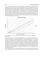
Fig.5(a) shows the I-V characteristics of the TJE-MOSFET vs. other devices (i.e., MOSFETs
and IGBTs) with the same n- drift thickness and doping level. The major advantages of the
TJE-MOSFET are its superior conduction characteristics compared with those of the existing
power devices. Normally, power MOSFETs are used in low-voltage and low current density
applications while IGBTs are used in high-voltage and high current density applications.
The TJE-MOSFET is very competitive in both applications.
As shown in Fig.5(a), the proposed the device (with p++/n++ doping levels of 8 x 10
19
) can
carry much higher current density than conventional power MOSFETs. For instance, at a
forward voltage drop of 1V, the TJE-MOSFET can carry 25x higher current density. At
higher voltage drops, the current density can be significantly higher. It also performs better
than a SJ MOSFET with a 2.5m pillar width at a forward voltage drop higher than 0.9V. As
described in the Introduction section, the SJ MOSFET requires accurately doped alternating
p and n pillars, the on-resistance of an SJ MOSFET can be reduced by orders of magnitude
compared to the conventional power MOSFET. However, higher voltage SJ MOSFETs are
not particularly easy to fabricate. For a 1000V-rated Super-junction device, a pillar height of
60m is needed. Creating such narrow and deep pillars which have exactly opposite doping
concentrations is very difficult using current semiconductor processing technology. The TJE-
MOSFET provides an alternative to create high performance power switches. The TJE-
MOSFET can share most of the processing techniques with conventional power MOSFETs or
IGBTs. However, additional steps are required to create the sharp and heavily-doped
p++/n++ metallurgical junction, which is challenging. The high thermal budgets of
conventional epitaxy methods for creating the n-drift layer and subsequent steps would
definitely alter the earlier created p++ and n++ layers; therefore, novel processing
techniques will be needed to address this challenge. For instance, a lightly-doped thin wafer
might be used as the voltage blocking layer instead of an epitaxially created n- drift layer.
Low-temperature epitaxial processes such as MBE might be required to create the p++ and
n++ layers.
Compared to IGBTs, the TJE-MOSFETs have superior forward conduction characteristics. At
the same current density, the forward voltage drop of the TJE-MOSFET is much smaller
than that of an IGBT. Furthermore, the TJE-MOSFET has no heel voltage as seen in an IGBT.
Fig.5(a) clearly shows that the TJE-MOSFET can carry 50A/cm
2
of current density at a
forward voltage drop of 0.7V while the current density of an IGBT is negligible at this
voltage. This means that the TJE-MOSFET can carry current right after a bias is applied
much like a MOSFET. Therefore, the TJE-MOSFET is more suitable than IGBTs in lower
current density applications. This also enables the parallelization of the TJE-MOSFET in
order to further improve the conduction characteristics. A trade-off between the forward
voltage drop and turn-off time is considered when designing an IGBT. Since the TJE-
MOSFET has a much lower forward voltage drop than an IGBT at the same current density,
there should be more flexibility to optimize between conduction loss and switching loss.
Furthermore, the simulations also suggest that the current density of the TJE-MOSFET can
be further improved by increasing the doping levels in the p++/n++ junction as shown in
Fig.5(b). This is due to the fact that band-to-band tunneling current is exponentially
proportional to the inverse of tunneling distance at a reverse-biased junction. The
improvement should only be restricted by the highest doping levels that can be reached in
these junctions.
Forward voltage drop (V)
0.0 0.2 0.4 0.6 0.8 1.0 1.2
Current density (A/cm
2
)
0
50
100
150
200
Proposed device
IGBT
Conventional MOSFET
Future SJ MOSFET (2.5m pillar)
(a)
Forward voltage drop (V)
0.0 0.2 0.4 0.6 0.8 1.0 1.2
Current density (A/cm
2
)
0
200
400
600
800
1000
Device #1 (8e19)
Device #2 (1e20)
Device #3 (2e20)
(b)
Reverse bias voltage (V)
0 100 200 300 400 500
Drain current (A/cm
2
)
0.00
0.01
0.02
0.03
0.04
0.05
TJE-MOSFET
IGBT
(c)
Fig.5 (a) I-V characteristics of the TJE-MOSFET vs. other power devices with same geometry
(b) I-V Characteristics comparison between the TJE-MOSFETs with various doping
concentrations at the p++/n++ junctions (c) Reverse characteristics comparison between the
THE-MOSFET and IGBT
This indicates that the TJE-MOSFET has the potential to outperform SJ MOSFETs at very
low current density levels in terms of conduction characteristics. Fig.5(c) shows the
breakdown characteristics of the TJE-MOSFET, which is very similar to the IGBT with
similar geometry and n- drift layer doping levels. It should be noted that the drift layer
doping levels in neither the TJE-MOSFET nor the IGBT were optimized and is taken a value
of 2 x 10
14
cm
-3
.
ConceptsofOptimizingPowerSemiconductor
DevicesUsingNovelNano-StructureforLowLosses 215
(a) (b)
Fig. 4 (a) Band energy diagram near the p++/n++ junction at equilibrium (b) Carrier
concentration during conduction
Fig.5(a) shows the I-V characteristics of the TJE-MOSFET vs. other devices (i.e., MOSFETs
and IGBTs) with the same n- drift thickness and doping level. The major advantages of the
TJE-MOSFET are its superior conduction characteristics compared with those of the existing
power devices. Normally, power MOSFETs are used in low-voltage and low current density
applications while IGBTs are used in high-voltage and high current density applications.
The TJE-MOSFET is very competitive in both applications.
As shown in Fig.5(a), the proposed the device (with p++/n++ doping levels of 8 x 10
19
) can
carry much higher current density than conventional power MOSFETs. For instance, at a
forward voltage drop of 1V, the TJE-MOSFET can carry 25x higher current density. At
higher voltage drops, the current density can be significantly higher. It also performs better
than a SJ MOSFET with a 2.5m pillar width at a forward voltage drop higher than 0.9V. As
described in the Introduction section, the SJ MOSFET requires accurately doped alternating
p and n pillars, the on-resistance of an SJ MOSFET can be reduced by orders of magnitude
compared to the conventional power MOSFET. However, higher voltage SJ MOSFETs are
not particularly easy to fabricate. For a 1000V-rated Super-junction device, a pillar height of
60m is needed. Creating such narrow and deep pillars which have exactly opposite doping
concentrations is very difficult using current semiconductor processing technology. The TJE-
MOSFET provides an alternative to create high performance power switches. The TJE-
MOSFET can share most of the processing techniques with conventional power MOSFETs or
IGBTs. However, additional steps are required to create the sharp and heavily-doped
p++/n++ metallurgical junction, which is challenging. The high thermal budgets of
conventional epitaxy methods for creating the n-drift layer and subsequent steps would
definitely alter the earlier created p++ and n++ layers; therefore, novel processing
techniques will be needed to address this challenge. For instance, a lightly-doped thin wafer
might be used as the voltage blocking layer instead of an epitaxially created n- drift layer.
Low-temperature epitaxial processes such as MBE might be required to create the p++ and
n++ layers.
Compared to IGBTs, the TJE-MOSFETs have superior forward conduction characteristics. At
the same current density, the forward voltage drop of the TJE-MOSFET is much smaller
than that of an IGBT. Furthermore, the TJE-MOSFET has no heel voltage as seen in an IGBT.
Fig.5(a) clearly shows that the TJE-MOSFET can carry 50A/cm
2
of current density at a
forward voltage drop of 0.7V while the current density of an IGBT is negligible at this
voltage. This means that the TJE-MOSFET can carry current right after a bias is applied
much like a MOSFET. Therefore, the TJE-MOSFET is more suitable than IGBTs in lower
current density applications. This also enables the parallelization of the TJE-MOSFET in
order to further improve the conduction characteristics. A trade-off between the forward
voltage drop and turn-off time is considered when designing an IGBT. Since the TJE-
MOSFET has a much lower forward voltage drop than an IGBT at the same current density,
there should be more flexibility to optimize between conduction loss and switching loss.
Furthermore, the simulations also suggest that the current density of the TJE-MOSFET can
be further improved by increasing the doping levels in the p++/n++ junction as shown in
Fig.5(b). This is due to the fact that band-to-band tunneling current is exponentially
proportional to the inverse of tunneling distance at a reverse-biased junction. The
improvement should only be restricted by the highest doping levels that can be reached in
these junctions.
Forward voltage drop (V)
0.0 0.2 0.4 0.6 0.8 1.0 1.2
Current density (A/cm
2
)
0
50
100
150
200
Proposed device
IGBT
Conventional MOSFET
Future SJ MOSFET (2.5m pillar)
(a)
Forward voltage drop (V)
0.0 0.2 0.4 0.6 0.8 1.0 1.2
Current density (A/cm
2
)
0
200
400
600
800
1000
Device #1 (8e19)
Device #2 (1e20)
Device #3 (2e20)
(b)
Reverse bias voltage (V)
0 100 200 300 400 500
Drain current (A/cm
2
)
0.00
0.01
0.02
0.03
0.04
0.05
TJE-MOSFET
IGBT
(c)
Fig.5 (a) I-V characteristics of the TJE-MOSFET vs. other power devices with same geometry
(b) I-V Characteristics comparison between the TJE-MOSFETs with various doping
concentrations at the p++/n++ junctions (c) Reverse characteristics comparison between the
THE-MOSFET and IGBT
This indicates that the TJE-MOSFET has the potential to outperform SJ MOSFETs at very
low current density levels in terms of conduction characteristics. Fig.5(c) shows the
breakdown characteristics of the TJE-MOSFET, which is very similar to the IGBT with
similar geometry and n- drift layer doping levels. It should be noted that the drift layer
doping levels in neither the TJE-MOSFET nor the IGBT were optimized and is taken a value
of 2 x 10
14
cm
-3
.
SemiconductorTechnologies216
3. Novel High Voltage SJ MOSFET Based on Porous Silicon Formation
3.1 Device Structure and Fabrication Process
A schematic of the trench gate type SJ MOSFET half unit cell based on porous silicon
formation is shown in Figure 6(a). A lightly doped (10
15
-10
16
cm
-3
depending on the targeted
pore size and pitch) n-type thin wafer (120-200 micron thick depending on voltage ratings)
is electrochemically etched to form deep macro-pores with small pore size and pitch though
most of the wafer thickness, leaving only a thin layer un-etched at the back side of the wafer.
Photo-assisted electro-chemical etching of silicon to form high-aspect-ratio microstructures
has been under development since the 1970s and has advanced to reach the level of
submicron precision (Coe, 1988; Chen, 1993).
n++ (by ion implantation or diffusion)
n- column
Drain electrode
p base
Gate electrode
oxide/dielectric
n++
Source electrode
p+
Polysilicon
source electrode
connected to
p polysilicon column
(created by filling the
etched macropores)
(a)
A1
A2
n- drift
p-
polySi
oxide
(b)
Fig. 6. (a) Schematic of the half unit-cell of the porous silicon based SJ; (b) Schematic of the
circular cell in hexagonal array topological design
This technique has been widely used in fabricating silicon-based photonic devices and
electronic devices, as well as micro-electro-mechanical systems (MEMS) (Theunissen, 1972;
Kleimann, et al., 2005; Charlton & Parker, 1997; Lehmann, et al., 1996; Wang, et al., 2003).
The pattern of the macro-pores is controlled by photolithography based on the cell
topological design (such as the simple linear trench design or the circular cell in hexagonal
array design as shown in Figure 6(b)). The pore size is controlled by the applied current
density and illumination intensity during etching. An n++ layer on the back side can then be
created by ion implantation or other standard doping method for the drain electrode. The
macro-pores are deposited with a thin conformal coating of oxide/dielectric layer using
standard microelectronic processes such as thermal oxidation or oxide-nitride-oxide (ONO)
deposition. The oxide/dielectric on the bottom of the macro-pores is then anisotropically
etched, leaving the oxide/dielectric layer only on the side walls of the macro-pores. Doped
p-type poly-silicon is deposited in the macro-pores to form the p region with the doping
level matching their sizes and pitches as well as the doping of the wafer. The poly-silicon
doping can be in situ doping or use a sequence of conformal poly deposition, tilted
implantation, poly refill and drive-in. These processes are sufficient for an aspect ratio as
large as 100. The p-type poly-silicon and the reminder of the n-type silicon between the
pores form the alternating p and n columns with a thin layer of oxide/dielectric layer on the
side walls. This oxide/dielectric layer prevents interdiffusion during the subsequent
processing steps. After the formation of the SJ structure and possibly a chemical-mechanical
polishing step, conventional ways of creating the power MOSFET structures including the
gate and source electrodes can be employed. This process can fabricate SJ structures with a
column size of a couple of microns and depth up to a couple of hundred microns, with the
potential to create SJ devices at voltages above 2000V.
3.2 Device Simulation Description
We have used physically-based device simulation software Synopsys Sentaurus Device to
perform the simulations. Fermi-Dirac statistics is employed in the carrier density
calculation. For low field bulk mobility, Klaassen’s unified mobility model (Klaassen, 1992;
Klaassen, 1992) is used, which considers the effects of lattice scattering, impurity scattering,
carrier-carrier scattering, and impurity clustering effects at high concentration. The mobility
degradation within the inversion layers is considered by employing Lombardi’s model
(Lombardi, et al., 1988) that accounts for the effects of surface acoustic phonon scattering
and surface roughness scattering. Canali’s model (Canali, et al., 1975) is used to account for
the carrier velocity saturation in high electric fields. Doping-dependent Shockley-Read-Hall
recombination and Auger recombination are considered. The breakdown of the device is
simulated by employing Lackner’s avalanche generation model (Lackner, 1991).
The device under consideration has a cell structure as shown in Figure 6(a) and uses the
topological design of a circular cell in a hexagonal array (Figure 6(b)). In order to satisfy the
charge compensation requirement, the size of the poly-silicon p columns and pitch of the p
columns are designed by
21
AnAp
, (1)
where p is the doping density in the p-type poly-silicon column and n is the wafer doping
density; A
1
and A
2
are the areas of the p-type poly-silicon and area of n-type silicon
surrounding the p-poly, respectively, as shown in Figure 6(b). The depths of the p and n
columns are taken as 160
m; p-base depth is 2.7
m and n+ source depth of 0.8
m, giving a
channel length of 1.9
m. The gate oxide thickness is 50nm. Gaussian profiles are assumed
for p-base and n+ source with the peak concentrations of 310
17
cm
-3
and 10
19
cm
-3
,
respectively. The thickness of the n-layer underneath the p and n columns is 5µm, and the
n+ drain doping is 10
19
cm
-3
. In the baseline half unit-cell, the width of the p-poly-silicon is
1
m, which is equivalent to a p-column diameter of 2
m. The thickness of the oxide layer
(between the p and n columns) and n-column width are 0.1
m and 0.692
m, respectively.
This makes the p-column center-to-center distance to be 3.6
m. The area ratio between the
poly-silicon p-column and the n-type silicon surround it, A
1
/A
2
, is then ½. The doping level
of the wafer is 910
15
cm
-3
and the doping level of the p-poly-silicon column is 1.810
16
cm
-3
. In
order to account for the cell topology of a circular cell in a hexagonal array, cylindrical
symmetry is assumed in the two-dimensional device simulations for the half unit cell.
3.3 Simulation Results and Discussion
Figure 7 shows the simulated breakdown and I-V characteristics of the baseline device. The
device has a breakdown voltage of 2490V and a specific on-resistance of 20m·cm
2
. The
specific on-resistance is calculated at the drain voltage of 0.5V by first evaluating the total
current within a 1 cm
2
device area. At this voltage, the silicon limit for conventional power
MOSFETs is 2600m·cm
2
by way of comparison.
ConceptsofOptimizingPowerSemiconductor
DevicesUsingNovelNano-StructureforLowLosses 217
3. Novel High Voltage SJ MOSFET Based on Porous Silicon Formation
3.1 Device Structure and Fabrication Process
A schematic of the trench gate type SJ MOSFET half unit cell based on porous silicon
formation is shown in Figure 6(a). A lightly doped (10
15
-10
16
cm
-3
depending on the targeted
pore size and pitch) n-type thin wafer (120-200 micron thick depending on voltage ratings)
is electrochemically etched to form deep macro-pores with small pore size and pitch though
most of the wafer thickness, leaving only a thin layer un-etched at the back side of the wafer.
Photo-assisted electro-chemical etching of silicon to form high-aspect-ratio microstructures
has been under development since the 1970s and has advanced to reach the level of
submicron precision (Coe, 1988; Chen, 1993).
n++ (by ion implantation or diffusion)
n- column
Drain electrode
p base
Gate electrode
oxide/dielectric
n++
Source electrode
p+
Polysilicon
source electrode
connected to
p polysilicon column
(created by filling the
etched macropores)
(a)
A1
A2
n- drift
p-
polySi
oxide
(b)
Fig. 6. (a) Schematic of the half unit-cell of the porous silicon based SJ; (b) Schematic of the
circular cell in hexagonal array topological design
This technique has been widely used in fabricating silicon-based photonic devices and
electronic devices, as well as micro-electro-mechanical systems (MEMS) (Theunissen, 1972;
Kleimann, et al., 2005; Charlton & Parker, 1997; Lehmann, et al., 1996; Wang, et al., 2003).
The pattern of the macro-pores is controlled by photolithography based on the cell
topological design (such as the simple linear trench design or the circular cell in hexagonal
array design as shown in Figure 6(b)). The pore size is controlled by the applied current
density and illumination intensity during etching. An n++ layer on the back side can then be
created by ion implantation or other standard doping method for the drain electrode. The
macro-pores are deposited with a thin conformal coating of oxide/dielectric layer using
standard microelectronic processes such as thermal oxidation or oxide-nitride-oxide (ONO)
deposition. The oxide/dielectric on the bottom of the macro-pores is then anisotropically
etched, leaving the oxide/dielectric layer only on the side walls of the macro-pores. Doped
p-type poly-silicon is deposited in the macro-pores to form the p region with the doping
level matching their sizes and pitches as well as the doping of the wafer. The poly-silicon
doping can be in situ doping or use a sequence of conformal poly deposition, tilted
implantation, poly refill and drive-in. These processes are sufficient for an aspect ratio as
large as 100. The p-type poly-silicon and the reminder of the n-type silicon between the
pores form the alternating p and n columns with a thin layer of oxide/dielectric layer on the
side walls. This oxide/dielectric layer prevents interdiffusion during the subsequent
processing steps. After the formation of the SJ structure and possibly a chemical-mechanical
polishing step, conventional ways of creating the power MOSFET structures including the
gate and source electrodes can be employed. This process can fabricate SJ structures with a
column size of a couple of microns and depth up to a couple of hundred microns, with the
potential to create SJ devices at voltages above 2000V.
3.2 Device Simulation Description
We have used physically-based device simulation software Synopsys Sentaurus Device to
perform the simulations. Fermi-Dirac statistics is employed in the carrier density
calculation. For low field bulk mobility, Klaassen’s unified mobility model (Klaassen, 1992;
Klaassen, 1992) is used, which considers the effects of lattice scattering, impurity scattering,
carrier-carrier scattering, and impurity clustering effects at high concentration. The mobility
degradation within the inversion layers is considered by employing Lombardi’s model
(Lombardi, et al., 1988) that accounts for the effects of surface acoustic phonon scattering
and surface roughness scattering. Canali’s model (Canali, et al., 1975) is used to account for
the carrier velocity saturation in high electric fields. Doping-dependent Shockley-Read-Hall
recombination and Auger recombination are considered. The breakdown of the device is
simulated by employing Lackner’s avalanche generation model (Lackner, 1991).
The device under consideration has a cell structure as shown in Figure 6(a) and uses the
topological design of a circular cell in a hexagonal array (Figure 6(b)). In order to satisfy the
charge compensation requirement, the size of the poly-silicon p columns and pitch of the p
columns are designed by
21
AnAp
, (1)
where p is the doping density in the p-type poly-silicon column and n is the wafer doping
density; A
1
and A
2
are the areas of the p-type poly-silicon and area of n-type silicon
surrounding the p-poly, respectively, as shown in Figure 6(b). The depths of the p and n
columns are taken as 160
m; p-base depth is 2.7
m and n+ source depth of 0.8
m, giving a
channel length of 1.9
m. The gate oxide thickness is 50nm. Gaussian profiles are assumed
for p-base and n+ source with the peak concentrations of 310
17
cm
-3
and 10
19
cm
-3
,
respectively. The thickness of the n-layer underneath the p and n columns is 5µm, and the
n+ drain doping is 10
19
cm
-3
. In the baseline half unit-cell, the width of the p-poly-silicon is
1
m, which is equivalent to a p-column diameter of 2
m. The thickness of the oxide layer
(between the p and n columns) and n-column width are 0.1
m and 0.692
m, respectively.
This makes the p-column center-to-center distance to be 3.6
m. The area ratio between the
poly-silicon p-column and the n-type silicon surround it, A
1
/A
2
, is then ½. The doping level
of the wafer is 910
15
cm
-3
and the doping level of the p-poly-silicon column is 1.810
16
cm
-3
. In
order to account for the cell topology of a circular cell in a hexagonal array, cylindrical
symmetry is assumed in the two-dimensional device simulations for the half unit cell.
3.3 Simulation Results and Discussion
Figure 7 shows the simulated breakdown and I-V characteristics of the baseline device. The
device has a breakdown voltage of 2490V and a specific on-resistance of 20m·cm
2
. The
specific on-resistance is calculated at the drain voltage of 0.5V by first evaluating the total
current within a 1 cm
2
device area. At this voltage, the silicon limit for conventional power
MOSFETs is 2600m·cm
2
by way of comparison.
SemiconductorTechnologies218
Drain
V
oltage (
V
)
Drain Current (A)
0 500 1000 1500 2000 2500
10
-13
10
-12
10
-11
10
-10
(a)
Drain
V
olta
g
e
(
V
)
Drain Current (A/cell)
0 1 2 3 4 5
0
5E-06
1E-05
1.5E-05
(b)
Fig. 7. Simulation results for baseline cell: (a) Breakdown characteristics; (b) I-V
characteristic at Vg=15V.
As aforementioned, the charges in the p and n columns need to be perfectly matched in
order to reach the highest breakdown voltage at certain n- and p-column doping levels. By
introducing an oxide layer between the p and n columns, interdiffusion between the two
regions during deposition and subsequent processing steps can be eliminated. Even so,
controlling the doping in the p-poly-silicon to exactly satisfy the charge balancing is very
challenging. It is useful to see how the charge imbalance in the p-poly-silicon would affect
the cell breakdown voltage. Simulations were first conducted to evaluate the breakdown
voltage variations with respect to the doping levels in the n-type silicon wafer while the
doping in the p-poly-silicon column is perfectly matched. The charge imbalance scenarios,
where the doping concentrations in the poly-silicon are taken as 5% or 10% above or below
the perfect matching levels, are then simulated. It can be seen in Figure 8(a), when a perfect
doping match is assumed, variations of doping in the wafer contribute little to the values of
the breakdown voltage (around 2500V for a column depth of 160
m) until a critical level is
reached. Above this level, the breakdown voltage decreases drastically due to the fact that
the p and n columns can no longer be fully depleted during reverse biasing. On the other
hand, if the doping level in the p-poly-silicon does not match the wafer, the breakdown
voltage decreases drastically as the doping in the wafer increases. A 10% imbalance leads to
a bigger reduction in breakdown voltage than a 5% imbalance at the same wafer doping
level. This result indicates process control for doping the p-poly-silicon is critical in creating
an ultra-high voltage MOSFET with ultra-low on-resistance. The doping imbalance is more
tolerable (less reduction in breakdown voltage) as the doping concentration in the wafer
gets lower.
However, lowering the doping concentration in the wafer leads to higher on-resistance (as
shown in Figure 8(b)). Consequently, if a certain level of charge imbalance in the p-poly-
silicon is inevitable, the doping concentration in the wafer has to be chosen such that a
trade-off between the breakdown voltage and the specific on-resistance can be reached.
Even with a small amount of charge imbalance, a properly designed device can still have far
better performance than a conventional one. For instance, starting from a wafer with a
doping level of 10
15
cm
-3
and assuming a 5% charge imbalance in the p poly-silicon, a
MOSFET with a breakdown voltage of 2100V and specific on-resistance of 410 m·cm
2
can
be produced. This is much better than the silicon limit of 1700 m·cm
2
at this voltage for a
conventional power MOSFET. Figure 3(c) shows the figures of merit (V
b
2
/R
on
A) for these
scenarios.
Doping in n silicon wafer (cm
-3
)
1e+15 1e+16
Breakdown Voltage (V)
0
500
1000
1500
2000
2500
Perfect match
90% match
95% match
105% match
110% match
(a)
Doping in n silicon wafer (cm
-3
)
0 5e+15 1e+16 2e+16 2e+16
Specific On-resistance (Ohm/cm
2
)
0.1
0.2
0.3
0.4
0.5
Perfect match
90% match
95% match
105% match
110% match
(b)
Doping in n silicon wafer (cm
-3
)
1e+15 1e+16
Figure of Merit (MW/cm
2
)
1
10
100
1000
Perfect match
90% match
95% match
105% match
110% match
(c)
Fig.3. (8) Breakdown voltage, (b) specific on-resistance, and (c) figure of merit vs. doping
concentration of silicon wafer for various charge imbalance conditions
It shows that a figure of merit of more than 500 MW/cm
2
is possible if perfect control of the
p-poly-doping can be achieved. A small amount of charge imbalance greatly reduces the
figure of merit. However, with a 5% charge imbalance, figures of merit between 10 and 30
MW/cm
2
are achievable for wafer doping levels between 10
15
to 10
16
cm
-3
, which covers
breakdown voltages between 2100 and 1000 V. This is still much better than the figures of
merit of silicon limits for conventional power MOSFETs, which are between 2.5 and 4
MW/cm
2
at these voltage ratings.
(a) (b)
Fig. 4 Comparison of the electron density distributions at 0.5V forward bias in the unit cell
and along the vertical axis through the center of n column between (a) wafer doping of
10
15
cm
-3
and (b) wafer doping of 910
15
cm
-3
. The oxide thickness between p and n column is
0.1
m.
ConceptsofOptimizingPowerSemiconductor
DevicesUsingNovelNano-StructureforLowLosses 219
Drain
V
oltage (
V
)
Drain Current (A)
0 500 1000 1500 2000 2500
10
-13
10
-12
10
-11
10
-10
(a)
Drain
V
olta
g
e
(
V
)
Drain Current (A/cell)
0 1 2 3 4 5
0
5E-06
1E-05
1.5E-05
(b)
Fig. 7. Simulation results for baseline cell: (a) Breakdown characteristics; (b) I-V
characteristic at Vg=15V.
As aforementioned, the charges in the p and n columns need to be perfectly matched in
order to reach the highest breakdown voltage at certain n- and p-column doping levels. By
introducing an oxide layer between the p and n columns, interdiffusion between the two
regions during deposition and subsequent processing steps can be eliminated. Even so,
controlling the doping in the p-poly-silicon to exactly satisfy the charge balancing is very
challenging. It is useful to see how the charge imbalance in the p-poly-silicon would affect
the cell breakdown voltage. Simulations were first conducted to evaluate the breakdown
voltage variations with respect to the doping levels in the n-type silicon wafer while the
doping in the p-poly-silicon column is perfectly matched. The charge imbalance scenarios,
where the doping concentrations in the poly-silicon are taken as 5% or 10% above or below
the perfect matching levels, are then simulated. It can be seen in Figure 8(a), when a perfect
doping match is assumed, variations of doping in the wafer contribute little to the values of
the breakdown voltage (around 2500V for a column depth of 160
m) until a critical level is
reached. Above this level, the breakdown voltage decreases drastically due to the fact that
the p and n columns can no longer be fully depleted during reverse biasing. On the other
hand, if the doping level in the p-poly-silicon does not match the wafer, the breakdown
voltage decreases drastically as the doping in the wafer increases. A 10% imbalance leads to
a bigger reduction in breakdown voltage than a 5% imbalance at the same wafer doping
level. This result indicates process control for doping the p-poly-silicon is critical in creating
an ultra-high voltage MOSFET with ultra-low on-resistance. The doping imbalance is more
tolerable (less reduction in breakdown voltage) as the doping concentration in the wafer
gets lower.
However, lowering the doping concentration in the wafer leads to higher on-resistance (as
shown in Figure 8(b)). Consequently, if a certain level of charge imbalance in the p-poly-
silicon is inevitable, the doping concentration in the wafer has to be chosen such that a
trade-off between the breakdown voltage and the specific on-resistance can be reached.
Even with a small amount of charge imbalance, a properly designed device can still have far
better performance than a conventional one. For instance, starting from a wafer with a
doping level of 10
15
cm
-3
and assuming a 5% charge imbalance in the p poly-silicon, a
MOSFET with a breakdown voltage of 2100V and specific on-resistance of 410 m·cm
2
can
be produced. This is much better than the silicon limit of 1700 m·cm
2
at this voltage for a
conventional power MOSFET. Figure 3(c) shows the figures of merit (V
b
2
/R
on
A) for these
scenarios.
Doping in n silicon wafer (cm
-3
)
1e+15 1e+16
Breakdown Voltage (V)
0
500
1000
1500
2000
2500
Perfect match
90% match
95% match
105% match
110% match
(a)
Doping in n silicon wafer (cm
-3
)
0 5e+15 1e+16 2e+16 2e+16
Specific On-resistance (Ohm/cm
2
)
0.1
0.2
0.3
0.4
0.5
Perfect match
90% match
95% match
105% match
110% match
(b)
Doping in n silicon wafer (cm
-3
)
1e+15 1e+16
Figure of Merit (MW/cm
2
)
1
10
100
1000
Perfect match
90% match
95% match
105% match
110% match
(c)
Fig.3. (8) Breakdown voltage, (b) specific on-resistance, and (c) figure of merit vs. doping
concentration of silicon wafer for various charge imbalance conditions
It shows that a figure of merit of more than 500 MW/cm
2
is possible if perfect control of the
p-poly-doping can be achieved. A small amount of charge imbalance greatly reduces the
figure of merit. However, with a 5% charge imbalance, figures of merit between 10 and 30
MW/cm
2
are achievable for wafer doping levels between 10
15
to 10
16
cm
-3
, which covers
breakdown voltages between 2100 and 1000 V. This is still much better than the figures of
merit of silicon limits for conventional power MOSFETs, which are between 2.5 and 4
MW/cm
2
at these voltage ratings.
(a) (b)
Fig. 4 Comparison of the electron density distributions at 0.5V forward bias in the unit cell
and along the vertical axis through the center of n column between (a) wafer doping of
10
15
cm
-3
and (b) wafer doping of 910
15
cm
-3
. The oxide thickness between p and n column is
0.1
m.
SemiconductorTechnologies220
It is shown in Figure 3(b) that the specific on-resistance increases with decreasing wafer
doping levels and it does not follow a linear relationship. Examination of the electron
density under forward-bias condition reveals that the nonlinear increase of the specific on-
resistance at lower wafer doping levels is due to the much more severe depletion in the n-
column, or JFET (Junction Field-Effect Transistor) effect. For instance, Figure 4(a) and (b)
show the comparison of the electron density distributions at a forward-bias of 0.5V for the
device with the wafer doping levels of 10
15
cm
-3
and 910
15
cm
-3
(baseline device), respectively.
The figure on the left shows the electron distribution over the half-unit cell. The white line
denotes the boundary of the depletion region. It can be seen that there is a depletion region
in the n-column along the oxide interface in both cases. The width of the depletion region
for a wafer doping of 10
15
cm
-3
is much larger than that for a wafer doping of 910
15
cm
-3
. The
figure on the right shows both the electron density and doping concentration distributions
along the center line of the n-column. It is clearly shown that the electron density in the n-
column is significantly lower than the doping concentration for the case of low wafer
doping of 10
15
cm
-3
; on the other hand, the electron density is kept at the doping level for the
case of high wafer doping of 910
15
cm
-3
. This explains why the on-resistance of the device
with a wafer doping of 10
15
cm
-3
is 21 times larger than the one with a wafer doping of
910
15
cm
-3
, while the doping level in the n-column is only 9 times smaller.
(a)
(b)
Fig. 5. Electron density distributions at 0.5V forward bias in the unit cell and along the
vertical axis through the center of n column for: (a) the case where the oxide thickness
between p and n column is 0.3
µm, and (b) the case of conventional SJ structure (no oxide
between p and n columns). The wafer doping level is 10
15
cm
-3
.
It can be said that the JFET effect is not a concern if high enough doping concentration is
used in the n and p columns. However, as aforementioned, if a small amount of charge
imbalance is inevitable, we have to reduce the wafer doping level in order to retain the high
breakdown voltage. In this case, the JFET effect greatly reduces the on-resistance of the
device. One way to partially alleviate this problem is to increase the thickness of the oxide
layer between the p and n columns. As the oxide thickness increases, the electrical field near
the oxide interface becomes smaller so that the depletion of the carriers in the nearby
regions becomes smaller. For example, Figure 5(a) shows the electron density distribution
for the device with a wafer doping level of 10
15
cm
-3
and an oxide thickness of 0.3 µm.
Compared to Figure 4(a), it is clearly shown that by increasing the oxide thickness from 0.l
µm to 0.3 µm, the depletion width is reduced and the electron density during forward-bias is
increased. This leads to lower specific on-resistance from 422 to 289 m
Ω·cm
2
, a 30%
reduction. We have also simulated the case of a conventional SJ MOSFET, where the oxide
layer is nonexistent. It turns out that, at the same wafer doping level of 10
15
cm
-3
, the JFET
effect is much more severe as shown in Figure 5(b); the specific on-resistance turns out to be
1084 mΩ·cm
2
, almost 4 times that of the device with a 0.3 µm oxide layer. Further
simulations on device breakdown have shown that adding an oxide layer between the p and
n columns has almost no effect on the breakdown voltage. This clearly shows that putting
an oxide layer between the p and n columns not only helps to prevent interdiffusion
between the columns during processing but increases the performance of the device as well
by reducing the JFET effect at lower wafer doping levels. This is important when charge
imbalance is expected and wafer doping is purposely reduced to maintain the device
breakdown voltage.
Oxide thickness (m)
0.0 0.1 0.2 0.3 0.4
Specific on-resistance (
cm
2
)
0.01
0.1
1
10
100
5e14
1e15
2e15
3e15
4e15
6e15
9e15
Fig. 6 On-resistance vs. oxide thickness for various wafer doping levels
Although a thicker oxide layer helps to reduce JFET effect, it does not carry any current like
the p-column; therefore, it creates a “dead” region in the device unit cell. This means the
oxide thickness needs to be optimized for each wafer doping level so that the lowest on-
resistance can be achieved. Figure 6 shows how the oxide thickness affects the specific on-
resistance of the device at various wafer doping levels. If a lower wafer doping level is to be
used, a larger width of oxide thickness would be needed. As the wafer doping level
increases toward its superjunction limit, the JFET effect becomes less of a concern and a
thinner oxide layer gives better on-resistance.
4. Conclusions and Future Directions
This chapter describes a novel concept for a mid-to-high voltage power semiconductor
switch that utilizes band-to-band tunneling and an avalanche injection mechanism.
Numerical simulations suggest the TJE-MOSFET has better forward conduction
characteristics than both IGBTs and power MOSFETs. The TJE-MOSFET can be very
competitive to MOSFETs and IGBTs in mid power range applications.
A promising method of making high-voltage SJ MOSFETs without costly epitaxial growth is
also described in this chapter. The charge compensating structures are created by etching
the structured macro-pores, followed by passivating the walls and filling the pores with
oppositely-charged poly-silicon. The effects of charge imbalance and the thickness of the
passivation layer are studied by physically-based numerical device simulations. It is found
ConceptsofOptimizingPowerSemiconductor
DevicesUsingNovelNano-StructureforLowLosses 221
It is shown in Figure 3(b) that the specific on-resistance increases with decreasing wafer
doping levels and it does not follow a linear relationship. Examination of the electron
density under forward-bias condition reveals that the nonlinear increase of the specific on-
resistance at lower wafer doping levels is due to the much more severe depletion in the n-
column, or JFET (Junction Field-Effect Transistor) effect. For instance, Figure 4(a) and (b)
show the comparison of the electron density distributions at a forward-bias of 0.5V for the
device with the wafer doping levels of 10
15
cm
-3
and 910
15
cm
-3
(baseline device), respectively.
The figure on the left shows the electron distribution over the half-unit cell. The white line
denotes the boundary of the depletion region. It can be seen that there is a depletion region
in the n-column along the oxide interface in both cases. The width of the depletion region
for a wafer doping of 10
15
cm
-3
is much larger than that for a wafer doping of 910
15
cm
-3
. The
figure on the right shows both the electron density and doping concentration distributions
along the center line of the n-column. It is clearly shown that the electron density in the n-
column is significantly lower than the doping concentration for the case of low wafer
doping of 10
15
cm
-3
; on the other hand, the electron density is kept at the doping level for the
case of high wafer doping of 910
15
cm
-3
. This explains why the on-resistance of the device
with a wafer doping of 10
15
cm
-3
is 21 times larger than the one with a wafer doping of
910
15
cm
-3
, while the doping level in the n-column is only 9 times smaller.
(a)
(b)
Fig. 5. Electron density distributions at 0.5V forward bias in the unit cell and along the
vertical axis through the center of n column for: (a) the case where the oxide thickness
between p and n column is 0.3
µm, and (b) the case of conventional SJ structure (no oxide
between p and n columns). The wafer doping level is 10
15
cm
-3
.
It can be said that the JFET effect is not a concern if high enough doping concentration is
used in the n and p columns. However, as aforementioned, if a small amount of charge
imbalance is inevitable, we have to reduce the wafer doping level in order to retain the high
breakdown voltage. In this case, the JFET effect greatly reduces the on-resistance of the
device. One way to partially alleviate this problem is to increase the thickness of the oxide
layer between the p and n columns. As the oxide thickness increases, the electrical field near
the oxide interface becomes smaller so that the depletion of the carriers in the nearby
regions becomes smaller. For example, Figure 5(a) shows the electron density distribution
for the device with a wafer doping level of 10
15
cm
-3
and an oxide thickness of 0.3 µm.
Compared to Figure 4(a), it is clearly shown that by increasing the oxide thickness from 0.l
µm to 0.3 µm, the depletion width is reduced and the electron density during forward-bias is
increased. This leads to lower specific on-resistance from 422 to 289 m
Ω·cm
2
, a 30%
reduction. We have also simulated the case of a conventional SJ MOSFET, where the oxide
layer is nonexistent. It turns out that, at the same wafer doping level of 10
15
cm
-3
, the JFET
effect is much more severe as shown in Figure 5(b); the specific on-resistance turns out to be
1084 mΩ·cm
2
, almost 4 times that of the device with a 0.3 µm oxide layer. Further
simulations on device breakdown have shown that adding an oxide layer between the p and
n columns has almost no effect on the breakdown voltage. This clearly shows that putting
an oxide layer between the p and n columns not only helps to prevent interdiffusion
between the columns during processing but increases the performance of the device as well
by reducing the JFET effect at lower wafer doping levels. This is important when charge
imbalance is expected and wafer doping is purposely reduced to maintain the device
breakdown voltage.
Oxide thickness (m)
0.0 0.1 0.2 0.3 0.4
Specific on-resistance (
cm
2
)
0.01
0.1
1
10
100
5e14
1e15
2e15
3e15
4e15
6e15
9e15
Fig. 6 On-resistance vs. oxide thickness for various wafer doping levels
Although a thicker oxide layer helps to reduce JFET effect, it does not carry any current like
the p-column; therefore, it creates a “dead” region in the device unit cell. This means the
oxide thickness needs to be optimized for each wafer doping level so that the lowest on-
resistance can be achieved. Figure 6 shows how the oxide thickness affects the specific on-
resistance of the device at various wafer doping levels. If a lower wafer doping level is to be
used, a larger width of oxide thickness would be needed. As the wafer doping level
increases toward its superjunction limit, the JFET effect becomes less of a concern and a
thinner oxide layer gives better on-resistance.
4. Conclusions and Future Directions
This chapter describes a novel concept for a mid-to-high voltage power semiconductor
switch that utilizes band-to-band tunneling and an avalanche injection mechanism.
Numerical simulations suggest the TJE-MOSFET has better forward conduction
characteristics than both IGBTs and power MOSFETs. The TJE-MOSFET can be very
competitive to MOSFETs and IGBTs in mid power range applications.
A promising method of making high-voltage SJ MOSFETs without costly epitaxial growth is
also described in this chapter. The charge compensating structures are created by etching
the structured macro-pores, followed by passivating the walls and filling the pores with
oppositely-charged poly-silicon. The effects of charge imbalance and the thickness of the
passivation layer are studied by physically-based numerical device simulations. It is found
SemiconductorTechnologies222
that even with a small amount of charge imbalance, the proposed method can still produce
high-voltage MOSFETs with much better performance than existing technology. A thick
oxide layer between the p and n columns is found to be helpful of alleviating the JFET
effects when the doping concentrations in the p and n columns are low. In comparison with
a conventional superjunction structure, the inclusion of an oxide layer between p and n
columns is found to help increase the device efficiency in addition to its ability to prevent
dopant interdiffusion.
5. References
Aydin, C., Zaslavsky, A., Luryi, S., Cristoloveanu, S., Mariolle, D., Fraboulet, D., and
Deleonibus, S. (2004). Lateral interband tunneling transistor in silicon-on-insulator.
Applied Physics Letters. vol. 84, no. 10, pp. 1780-1782.
Canali, C., Majni, G., Minder, R., and Ottaviani, G. (1975). Electron and Hole Drift Velocity
Measurements in Silicon and Their Empirical Relation to Electric Field and
Temperature. IEEE Transactions on Electron Devices. vol. 22, no. 11, pp. 1045-1047.
Charlton, M.D.B. and Parker, G.J. (1997). Fabrication of High Aspect Ratio Silicon
Microstructures by Anodic Etching. Journal of Micromechanics and Microengineering.
vol. 7, pp.155-158.
Chen, X. (1993)Semiconductor power devices with alternating conductivity type high-
voltage breakdown regions. US Patent 5216275.
Chen, Y., and Liang, Y. C. (2007). Design of Gradient Oxide-Bypassed Superjunction Power
MOSFETE Devices. IEEE Transactions on Power Electronics, vol. 22, no. 4, pp. 1303-
1310.
Coe, D. J. (1998). High voltage semiconductor device. US Patent 4754310.
Deboy, G., März, M., Stengle, J P., Strack, H., Tihanyi, J., and Weber, H. (1998). A new
generation of high voltage MOSFETs breaks the limit line of silicon. Technical Digest
of IEDM 98, Dec. 1998, pp. 683-685.
Fujihira, T. (1997). Theory of Semiconductor Superjunction Devices. Japan Journal of Applied
Physcis, vol. 36, no.10, pp. 6254-6262.
Gan, K. P., Liang, Y. C., Samudra, G. S., and Yong, L. (2001). A Simple Technology for
Superjunction Device Fabrication: Polyflanked VDMOSFET. IEEE Electron Device
Letters, vol. 22, no. 8, pp. 407-409.
Hu, C. (1979). Optimum doping profile for minimum ohmic resistance and high-breakdown
voltage. IEEE Transactions on Electron Devices, vol. 26, no. 3, pp. 243-244.
Klaassen, D. B. M. (1992). A unified mobility model for device simulation I. Model
equations and concentration dependence. Solid-State Electron. vol. 35, no. 7, pp. 953-
959.
Klaassen, D. B. M. (1992). A unified mobility model for device simulation II. Temperature
dependence of carrier mobility and lifetime. Solid-State Electron. vol. 35, no. 7, pp.
961-967.
Kleimann, P., Badel, X., and Linnros, J. (2005). Toward the Formation of Three-Dimensional
Nanostructures by Electrochemical Etching of Silicon. Applied Physics Letters. vol.
86, pp.183108.
Lackner, T. (1991). Avalanche Multiplication in Semiconductors: A Modification of
Chynoweth's Law. Solid-State Electron. vol. 34, no. 1, pp. 33-42.
Lehmann, V., Honlein, W., Reisinger, H., Spitzer, A., Wendt, H., and Willer, J. (1996). A
Novel Capacitor Technology Based on Porous Silicon. Thin Solid Films. vol.276,
pp.138-142.
Liang, Y. C., Gan, K. P., and Samudra, G. S. (2001). Oxide-bypassed VDMOS (OBVDMOS):
An alternative to superjunction high voltage MOS power devices. IEEE Electron
Device Letters. vol. 22, no. 8, pp. 407-409.
Lombardi, C., Manzini, S., Saporito, A., and Vanzi, M. (1988). A physically based mobility
model for numerical simulation of nonplanar devices. Computer-Aided Design of
Integrated Circuits and Systems, IEEE Transactions on. vol. 7, no. 11, pp. 1164-1171.
Minato, T., Nitta, T., Uenisi, A., Yano, M., Harada, M., and Hine, S. (2000). Which is cooler,
Trench or Multi-Epitaxy. in Proc.of the 12th International Symposium on Power
Semiconductor Devices and ICs, Toulous, France: pp. 73-76, 2000.
Miura, Y., Ninomiya, H., and Kobayashi, K. (2005). High Performance Superjunction
UMOSFETs with Split P-Colums Fabricated by Multi-Ion-Implantations. in Proc.of
the 17th International Symposium on Power Semiconductor Devices & IC's, Santa
Barbara, CA: pp. 1-4.
Onishi, Y., Iwamoto, S., Sato, T., Nagaoka, T., Ueno, K., and Fujihira, T. (2002). 24 m�cm2
680 V silicon superjunction MOSFET. in Proc.of the 14th International Symposium on
Power Semiconductor Devices and ICs, pp. 241-244.
Rochefort, C., van Dalen, R., Duhayon, N., and Vandervorst, W. (2002). Manufacturing of
high aspect-ratio p-n junctions using vapor phase doping for application in multi-
Resurf devices. in Proc.of the 14th International Symposium on Power Semiconductor
Devices and ICs, pp. 237-240, 2002.
Rub, M., Bar, M., Deboy, G., Niedernostheide, F. J., Schmitt, M., Schulze, H. J., and
Willmeroth, A. (2004). 550V Superjunction 3.9mm2 Transistor Formed by 25 MeV
Masked Boron Implantation. in Proc.of the 16th International Symposium on Power
Semiconductor Devices & IC's, Kitakyushu, Japan: pp. 445-458.
Shenoy, P.M., Bhalla, A., and Dolny, G.M. (1999). Analysis of the Effect of Charge Imbalance
on the Static and Dynamic Characteristics of the Super Junction MOSFET.
Proceedings of ISPSD’99, May 1999, pp. 99-102.
Solomon, P. M., Frank, D. J., D'Emic, C., Dokumaci, O., Ronsheim, P., and Haensch, W. E.,
Universal tunneling behavior in technologically relevant P/N junction diodes.
Journal of Applied Physics. vol. 95, no. 10, pp. 5800-5812.
Theunissen, M.J.J. (1972). Etch Channel Formation during Anodic Dissolution of N-Type
Silicon in Aqueous Hydrofluoric Acid. Solid-State Science and Technology. vol.119,
no. 3, pp.351-360.
von Borany, J., Friedrich, M., Rüb, M., Deboy, G., Butschke, J., and Letzkus, F. (2004).
Application of Ultra-High Energy Boron Implantation for Superjunction Power
(CoolMOS TM) Devices. Nuclear Inst. and Methods in Physics Research, B, vol. 237, no.
1-2, pp. 62-67.
W. Saito, I. Omura, S. Aida, S. Koduki, M. Izumisawa, H. Yoshioka, and T. Ogura, "Over
1000V Semi-Superjunction MOSFET with Ultra-Low On-Resistance Blow the Si-
Limit," in Proc.of 17th International Symposium on Power Semiconductor Device &
IC's, Santa Barbara, CA: 2005.
ConceptsofOptimizingPowerSemiconductor
DevicesUsingNovelNano-StructureforLowLosses 223
that even with a small amount of charge imbalance, the proposed method can still produce
high-voltage MOSFETs with much better performance than existing technology. A thick
oxide layer between the p and n columns is found to be helpful of alleviating the JFET
effects when the doping concentrations in the p and n columns are low. In comparison with
a conventional superjunction structure, the inclusion of an oxide layer between p and n
columns is found to help increase the device efficiency in addition to its ability to prevent
dopant interdiffusion.
5. References
Aydin, C., Zaslavsky, A., Luryi, S., Cristoloveanu, S., Mariolle, D., Fraboulet, D., and
Deleonibus, S. (2004). Lateral interband tunneling transistor in silicon-on-insulator.
Applied Physics Letters. vol. 84, no. 10, pp. 1780-1782.
Canali, C., Majni, G., Minder, R., and Ottaviani, G. (1975). Electron and Hole Drift Velocity
Measurements in Silicon and Their Empirical Relation to Electric Field and
Temperature. IEEE Transactions on Electron Devices. vol. 22, no. 11, pp. 1045-1047.
Charlton, M.D.B. and Parker, G.J. (1997). Fabrication of High Aspect Ratio Silicon
Microstructures by Anodic Etching. Journal of Micromechanics and Microengineering.
vol. 7, pp.155-158.
Chen, X. (1993)Semiconductor power devices with alternating conductivity type high-
voltage breakdown regions. US Patent 5216275.
Chen, Y., and Liang, Y. C. (2007). Design of Gradient Oxide-Bypassed Superjunction Power
MOSFETE Devices. IEEE Transactions on Power Electronics, vol. 22, no. 4, pp. 1303-
1310.
Coe, D. J. (1998). High voltage semiconductor device. US Patent 4754310.
Deboy, G., März, M., Stengle, J P., Strack, H., Tihanyi, J., and Weber, H. (1998). A new
generation of high voltage MOSFETs breaks the limit line of silicon. Technical Digest
of IEDM 98, Dec. 1998, pp. 683-685.
Fujihira, T. (1997). Theory of Semiconductor Superjunction Devices. Japan Journal of Applied
Physcis, vol. 36, no.10, pp. 6254-6262.
Gan, K. P., Liang, Y. C., Samudra, G. S., and Yong, L. (2001). A Simple Technology for
Superjunction Device Fabrication: Polyflanked VDMOSFET. IEEE Electron Device
Letters, vol. 22, no. 8, pp. 407-409.
Hu, C. (1979). Optimum doping profile for minimum ohmic resistance and high-breakdown
voltage. IEEE Transactions on Electron Devices, vol. 26, no. 3, pp. 243-244.
Klaassen, D. B. M. (1992). A unified mobility model for device simulation I. Model
equations and concentration dependence. Solid-State Electron. vol. 35, no. 7, pp. 953-
959.
Klaassen, D. B. M. (1992). A unified mobility model for device simulation II. Temperature
dependence of carrier mobility and lifetime. Solid-State Electron. vol. 35, no. 7, pp.
961-967.
Kleimann, P., Badel, X., and Linnros, J. (2005). Toward the Formation of Three-Dimensional
Nanostructures by Electrochemical Etching of Silicon. Applied Physics Letters. vol.
86, pp.183108.
Lackner, T. (1991). Avalanche Multiplication in Semiconductors: A Modification of
Chynoweth's Law. Solid-State Electron. vol. 34, no. 1, pp. 33-42.
Lehmann, V., Honlein, W., Reisinger, H., Spitzer, A., Wendt, H., and Willer, J. (1996). A
Novel Capacitor Technology Based on Porous Silicon. Thin Solid Films. vol.276,
pp.138-142.
Liang, Y. C., Gan, K. P., and Samudra, G. S. (2001). Oxide-bypassed VDMOS (OBVDMOS):
An alternative to superjunction high voltage MOS power devices. IEEE Electron
Device Letters. vol. 22, no. 8, pp. 407-409.
Lombardi, C., Manzini, S., Saporito, A., and Vanzi, M. (1988). A physically based mobility
model for numerical simulation of nonplanar devices. Computer-Aided Design of
Integrated Circuits and Systems, IEEE Transactions on. vol. 7, no. 11, pp. 1164-1171.
Minato, T., Nitta, T., Uenisi, A., Yano, M., Harada, M., and Hine, S. (2000). Which is cooler,
Trench or Multi-Epitaxy. in Proc.of the 12th International Symposium on Power
Semiconductor Devices and ICs, Toulous, France: pp. 73-76, 2000.
Miura, Y., Ninomiya, H., and Kobayashi, K. (2005). High Performance Superjunction
UMOSFETs with Split P-Colums Fabricated by Multi-Ion-Implantations. in Proc.of
the 17th International Symposium on Power Semiconductor Devices & IC's, Santa
Barbara, CA: pp. 1-4.
Onishi, Y., Iwamoto, S., Sato, T., Nagaoka, T., Ueno, K., and Fujihira, T. (2002). 24 m�cm2
680 V silicon superjunction MOSFET. in Proc.of the 14th International Symposium on
Power Semiconductor Devices and ICs, pp. 241-244.
Rochefort, C., van Dalen, R., Duhayon, N., and Vandervorst, W. (2002). Manufacturing of
high aspect-ratio p-n junctions using vapor phase doping for application in multi-
Resurf devices. in Proc.of the 14th International Symposium on Power Semiconductor
Devices and ICs, pp. 237-240, 2002.
Rub, M., Bar, M., Deboy, G., Niedernostheide, F. J., Schmitt, M., Schulze, H. J., and
Willmeroth, A. (2004). 550V Superjunction 3.9mm2 Transistor Formed by 25 MeV
Masked Boron Implantation. in Proc.of the 16th International Symposium on Power
Semiconductor Devices & IC's, Kitakyushu, Japan: pp. 445-458.
Shenoy, P.M., Bhalla, A., and Dolny, G.M. (1999). Analysis of the Effect of Charge Imbalance
on the Static and Dynamic Characteristics of the Super Junction MOSFET.
Proceedings of ISPSD’99, May 1999, pp. 99-102.
Solomon, P. M., Frank, D. J., D'Emic, C., Dokumaci, O., Ronsheim, P., and Haensch, W. E.,
Universal tunneling behavior in technologically relevant P/N junction diodes.
Journal of Applied Physics. vol. 95, no. 10, pp. 5800-5812.
Theunissen, M.J.J. (1972). Etch Channel Formation during Anodic Dissolution of N-Type
Silicon in Aqueous Hydrofluoric Acid. Solid-State Science and Technology. vol.119,
no. 3, pp.351-360.
von Borany, J., Friedrich, M., Rüb, M., Deboy, G., Butschke, J., and Letzkus, F. (2004).
Application of Ultra-High Energy Boron Implantation for Superjunction Power
(CoolMOS TM) Devices. Nuclear Inst. and Methods in Physics Research, B, vol. 237, no.
1-2, pp. 62-67.
W. Saito, I. Omura, S. Aida, S. Koduki, M. Izumisawa, H. Yoshioka, and T. Ogura, "Over
1000V Semi-Superjunction MOSFET with Ultra-Low On-Resistance Blow the Si-
Limit," in Proc.of 17th International Symposium on Power Semiconductor Device &
IC's, Santa Barbara, CA: 2005.
SemiconductorTechnologies224
Wang, L., Nichelatti, A., Schellevis, H., de Boer, C., Visser, C., Nguyen, T.N., and Sarro, P.M.
(2003). High Aspect Ratio Through-Wafer Interconnections for 3D-Microsystems.
Proc. of IEEE MEMS-03 Kyoto, pp.634-637.
Ye, H. and Haldar, P., (2008). A MOS Gated Power Semiconductor Switch Using Band-to-
Band Tunneling and Avalanche Injection Mechanism. IEEE Trans. On Electron
Devices. Vol.55, No.6, pp.1524-1528.
Ye, H. and Haldar, P. (2008). Optimization of the Porous Silicon Based Superjunction Power
MOSFET. IEEE Trans. On Electron Devices. Vol.55, No.8, pp.2246-2251.
TheCriticalFeedbackLevelinNanostructure-BasedSemiconductorLasers 225
The Critical Feedback Level in Nanostructure-Based Semiconductor
Lasers
F.Grillot,N.A.Naderi,M.Pochet,C Y.LinandL.F.Lester
x
The Critical Feedback Level in Nanostructure-
Based Semiconductor Lasers
F. Grillot
(1)(2)
, N. A. Naderi
(2)
, M. Pochet
(2)
, C Y. Lin
(2)
and L. F. Lester
(2)
(1) Université Européenne de Bretagne, CNRS, Laboratoire Foton, INSA de Rennes, 20
Avenue des Buttes de Coësmes, 35708 Rennes, Cedex 7, France
(2) Center for High Technology Materials, The University of New Mexico, 1313 Goddard
SE, Albuquerque, United States
1. Introduction
The extension of optical networks to local residential subscribers requires the development
of extremely low-cost laser transmitter sources (Tohmori et al., 1997). While wafer
fabrication allows for large-scale production, which drastically reduces the cost per laser,
packaging remains a cost bottleneck, as it is not supported by parallel processing. Cost
reduction must therefore be based on packaging simplification, such as flip-chip bonding
and direct coupling of the laser into the fiber (Fernier et al., 1998). One of the characteristic
problems of semiconductor lasers that complicates packaging is their sensitivity to external
optical feedback. Fiber optic communication systems can be limited by unwanted optical
feedback arising at fiber facets and junctions (Clarke, 1991), (Kitaoka et al., 1996). Although
Faraday isolators are used extensively to reduce back reflections by as much as 60-dB, the
elimination of the optical isolator remains a big challenge and is desirable because it leads to
simplified packaging and will greatly reduce cost (Grillot et al., 2002). To understand the
conditions under which the isolator can be eliminated, it is instructive to briefly review the
physics of feedback in semiconductor lasers. This investigation naturally leads to
highlighting the particular advantages of nanostructures in altering or improving the
feedback resistance of the device.
The performance of a semiconductor laser can be strongly altered by external optical
feedback. During early research, the importance of the distance between the laser facet and
an external mirror reflector was pointed out in determining the nature of the semiconductor
laser’s response to optical feedback (Hirota & Suematsu, 1979). Even small reflections in the
percent range were found to affect the laser stability dramatically. Although external optical
feedback can be considered as a source of instability in many situations, it also can produce
several beneficial effects that can improve laser performance. At the extremes of very weak
and very strong optical feedback, linewidth narrowing and noise suppression can occur.
This advantage, along with the large gain bandwidth of the semiconductor laser, can
produce a highly tunable, narrow linewidth source that attracts many applications in
spectroscopy, metrology and telecommunications (Kane & Shore, 2005).
10
SemiconductorTechnologies226
Five distinct regimes based on spectral observation were reported for 1.55-µm distributed
feedback (DFB) semiconductor lasers (Tkach & Chraplyvy, 1986). At the lowest feedback
level, regime I, the laser operates on a single external cavity mode that emerges from the
solitary laser mode. Depending on the phase of the feedback, the laser linewidth can be
narrowed or broadened. Within regime II, the mode appears to split into two modes arising
from rapid mode hopping. Noise-induced hopping between two external cavity modes is
the underlying reason for this behavior. The transition to regime II has been shown to
correspond to multiple solutions to the steady state equation that determines the frequency
of the laser. This condition is satisfied when the parameter X
F
is equal to unity in the
following expression:
X
F
K
F
e
1
H
2
(1)
where
e
is the external cavity roundtrip time while
K
F
2C
i
R
p
is denoted as the
feedback parameter. R
P
is the feedback ratio and is defined as
R
P
P
1
P
0
(with P
1
the power
returned to the facet and P
0
the emitted power), C is the coupling coefficient from the laser
facet to the external cavity, and
i
is the internal roundtrip time within the laser cavity. The
so-called linewidth enhancement factor (
H
-factor) corresponding to the coupling between
the phase and the amplitude of the electric field is usually defined as follows:
H
4
dn dN
dg dN
4
dn dN
dG
ne
t
dN
(2)
where g is the material gain. The α
H
-factor depends on the ratio of the evolution of the
refractive index n with the carrier density N to that of the differential gain dg/dn. Γ is the
optical confinement factor and G
net
=Γg-α
i
is the net modal gain where α
i
is the internal loss
coefficient. The
H
-factor is used to distinguish the behavior of semiconductor lasers with
respect to other types of lasers (Henry, 1982), and influences several fundamental aspects of
semiconductor lasers, such as the linewidth (Su et al., 2004) and the laser behavior under
optical feedback (Su et al., 2003). In regime III the laser re-stabilizes in a single external
cavity mode (the lowest linewidth mode) with constant power. As the feedback level is
further increased, the impact of optical feedback becomes independent of the external cavity
length and the laser undergoes a transition to a chaotic state characterized by coherence
collapse (CC) and denoted as regime IV (Lenstra et al., 1985). Coherence collapse or critical
feedback is the common name given to describe the irregular dynamics occurring when the
laser is operated above threshold, and has been greatly studied over the last twenty years.
This regime has been described as co-existing chaotic attractors (Mork et al., 1988) and as an
important source of noise (Mork et al., 1988), (Tromborg & Mork, 1990). The main
consequence of the coherence collapse regime consists of a drastic collapse of the laser’s
coherence time leading to an enhancement of the laser’s linewidth up to several gigahertz.
For lasers used as an optical transmitter, the coherence collapse has been experimentally
(Grillot et al., 2002) and theoretically (Clarke, 1991) demonstrated to cause a strong
degradation in the bit error rate (BER). As the feedback level is further increased, the laser
enters regime V, which is characterized by single-mode, constant intensity and narrow
linewidth operation. This regime can only be reached when laser diodes with antireflection
coated facets are used.
The purpose of this chapter is to show both theoretically and experimentally that the
variations of the above-threshold
H
-factor negatively impact the feedback level for which
the coherence collapse regime occurs. The coherence collapse threshold is explored in
nanostructure based semiconductor lasers, which in the context of this work encompasses
quantum dot (QD), quantum dash (QDash), and quantum well (QW) structures. It is
particularly well-known that QD and QDash based semiconductor lasers have attracted a lot
of interest in the last decade owing to their expected remarkable properties arising from
charge carrier confinement in the three space dimensions (Arakawa & Sakaki, 1982). Indeed,
low threshold current densities and high material gain (Bimberg et al., 1997), (Liu et al.,
1999), temperature insensitivity (Deppe et al., 2002), and reduced
H
-factor at the lasing
wavelength (Saito et al., 2000), (Martinez et al., 2005) have been reported. This latter
property combined with a high damping factor (O’Brien et al., 2003), (Erneux et al., 2008)
was found to be of utmost importance because it should increase the tolerance to optical
feedback in these devices (Azouigui et al., 2007), (Su et al., 2003) and may also offer potential
advantages for direct modulation without transmission dispersion penalty.
However, in some cases, the above-threshold
H
-factor was experimentally found to be
much larger as compared to traditional QW lasers (
a
Grillot et al., 2008), (Dagens et al., 2005).
Such an enhancement is naturally not beneficial in practice for many reasons (Henry, 1982)
and it provokes a rapid collapse of the laser’s coherence time. Thus, considering the energy
level contributions such as the ground state (GS) and the excited state (ES), this chapter
shows that the analytical relation giving the onset of the critical feedback level can be
rewritten. The carrier filling from the ES is found to produce an additional term, which
accelerates the route to chaos. Also depending on how the above-threshold
H
-factor
behaves, the critical feedback level can exhibit two different trends with output power.
Thus, the influence of the ES coupled to the emphasized non-linear effects makes such
devices more sensitive to optical feedback causing larger variations in the onset of the
coherence collapse. These results highlight that the control of the
H
-factor has to be
considered as a significant input for the realization of feedback-resistant lasers. It is also
pointed out that the prediction of the onset of the coherence collapse remains an important
feature for all applications requiring a low noise level or a proper control of the laser
coherence.
2. Predicting the onset of the critical feedback regime
Different analytical models giving the onset of the coherence collapse have been derived
over the last twenty years. This section aims to provide an overview of the most relevant
relations estimating this critical feedback level.
2.1 Optical Power Transfer Function Analysis
This model was derived from the microwave modulation characteristics of laser diodes
(Helms & Petermann, 1989). Starting from the conventional rate equations for a single-
mode laser diode with optical feedback evaluated through small-signal analysis, it was
shown that the modulation transfer function of a feedback laser can be expressed as:
TheCriticalFeedbackLevelinNanostructure-BasedSemiconductorLasers 227
Five distinct regimes based on spectral observation were reported for 1.55-µm distributed
feedback (DFB) semiconductor lasers (Tkach & Chraplyvy, 1986). At the lowest feedback
level, regime I, the laser operates on a single external cavity mode that emerges from the
solitary laser mode. Depending on the phase of the feedback, the laser linewidth can be
narrowed or broadened. Within regime II, the mode appears to split into two modes arising
from rapid mode hopping. Noise-induced hopping between two external cavity modes is
the underlying reason for this behavior. The transition to regime II has been shown to
correspond to multiple solutions to the steady state equation that determines the frequency
of the laser. This condition is satisfied when the parameter X
F
is equal to unity in the
following expression:
X
F
K
F
e
1
H
2
(1)
where
e
is the external cavity roundtrip time while
K
F
2C
i
R
p
is denoted as the
feedback parameter. R
P
is the feedback ratio and is defined as
R
P
P
1
P
0
(with P
1
the power
returned to the facet and P
0
the emitted power), C is the coupling coefficient from the laser
facet to the external cavity, and
i
is the internal roundtrip time within the laser cavity. The
so-called linewidth enhancement factor (
H
-factor) corresponding to the coupling between
the phase and the amplitude of the electric field is usually defined as follows:
H
4
dn dN
dg dN
4
dn dN
dG
ne
t
dN
(2)
where g is the material gain. The α
H
-factor depends on the ratio of the evolution of the
refractive index n with the carrier density N to that of the differential gain dg/dn. Γ is the
optical confinement factor and G
net
=Γg-α
i
is the net modal gain where α
i
is the internal loss
coefficient. The
H
-factor is used to distinguish the behavior of semiconductor lasers with
respect to other types of lasers (Henry, 1982), and influences several fundamental aspects of
semiconductor lasers, such as the linewidth (Su et al., 2004) and the laser behavior under
optical feedback (Su et al., 2003). In regime III the laser re-stabilizes in a single external
cavity mode (the lowest linewidth mode) with constant power. As the feedback level is
further increased, the impact of optical feedback becomes independent of the external cavity
length and the laser undergoes a transition to a chaotic state characterized by coherence
collapse (CC) and denoted as regime IV (Lenstra et al., 1985). Coherence collapse or critical
feedback is the common name given to describe the irregular dynamics occurring when the
laser is operated above threshold, and has been greatly studied over the last twenty years.
This regime has been described as co-existing chaotic attractors (Mork et al., 1988) and as an
important source of noise (Mork et al., 1988), (Tromborg & Mork, 1990). The main
consequence of the coherence collapse regime consists of a drastic collapse of the laser’s
coherence time leading to an enhancement of the laser’s linewidth up to several gigahertz.
For lasers used as an optical transmitter, the coherence collapse has been experimentally
(Grillot et al., 2002) and theoretically (Clarke, 1991) demonstrated to cause a strong
degradation in the bit error rate (BER). As the feedback level is further increased, the laser
enters regime V, which is characterized by single-mode, constant intensity and narrow
linewidth operation. This regime can only be reached when laser diodes with antireflection
coated facets are used.
The purpose of this chapter is to show both theoretically and experimentally that the
variations of the above-threshold
H
-factor negatively impact the feedback level for which
the coherence collapse regime occurs. The coherence collapse threshold is explored in
nanostructure based semiconductor lasers, which in the context of this work encompasses
quantum dot (QD), quantum dash (QDash), and quantum well (QW) structures. It is
particularly well-known that QD and QDash based semiconductor lasers have attracted a lot
of interest in the last decade owing to their expected remarkable properties arising from
charge carrier confinement in the three space dimensions (Arakawa & Sakaki, 1982). Indeed,
low threshold current densities and high material gain (Bimberg et al., 1997), (Liu et al.,
1999), temperature insensitivity (Deppe et al., 2002), and reduced
H
-factor at the lasing
wavelength (Saito et al., 2000), (Martinez et al., 2005) have been reported. This latter
property combined with a high damping factor (O’Brien et al., 2003), (Erneux et al., 2008)
was found to be of utmost importance because it should increase the tolerance to optical
feedback in these devices (Azouigui et al., 2007), (Su et al., 2003) and may also offer potential
advantages for direct modulation without transmission dispersion penalty.
However, in some cases, the above-threshold
H
-factor was experimentally found to be
much larger as compared to traditional QW lasers (
a
Grillot et al., 2008), (Dagens et al., 2005).
Such an enhancement is naturally not beneficial in practice for many reasons (Henry, 1982)
and it provokes a rapid collapse of the laser’s coherence time. Thus, considering the energy
level contributions such as the ground state (GS) and the excited state (ES), this chapter
shows that the analytical relation giving the onset of the critical feedback level can be
rewritten. The carrier filling from the ES is found to produce an additional term, which
accelerates the route to chaos. Also depending on how the above-threshold
H
-factor
behaves, the critical feedback level can exhibit two different trends with output power.
Thus, the influence of the ES coupled to the emphasized non-linear effects makes such
devices more sensitive to optical feedback causing larger variations in the onset of the
coherence collapse. These results highlight that the control of the
H
-factor has to be
considered as a significant input for the realization of feedback-resistant lasers. It is also
pointed out that the prediction of the onset of the coherence collapse remains an important
feature for all applications requiring a low noise level or a proper control of the laser
coherence.
2. Predicting the onset of the critical feedback regime
Different analytical models giving the onset of the coherence collapse have been derived
over the last twenty years. This section aims to provide an overview of the most relevant
relations estimating this critical feedback level.
2.1 Optical Power Transfer Function Analysis
This model was derived from the microwave modulation characteristics of laser diodes
(Helms & Petermann, 1989). Starting from the conventional rate equations for a single-
mode laser diode with optical feedback evaluated through small-signal analysis, it was
shown that the modulation transfer function of a feedback laser can be expressed as: