Advances in Analog Circuits Part 12 doc
Bạn đang xem bản rút gọn của tài liệu. Xem và tải ngay bản đầy đủ của tài liệu tại đây (2.07 MB, 30 trang )
Analog Circuit for Motion Detection Applied to Target Tracking System
319
L
1
Time t
Motion
signal
P
1
P
2
EMD
V
E
L
1
L
2
D
C
D
Time t
C
(
V
E
)
Time t
P : Photoreceptor
L : Large monopolar cell
D : Delay neuron
C : Correlator
v
Targ et
P
1
Time t
L
2
Time t
P
2
Time t
(a)
(b)
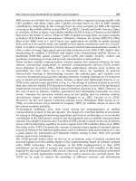
Fig. 1. Unit model for motion detection. (a) Model. (b) Transient response of each cell.
and V
D
and I
D
are decreased by MN
2
. The current I
C
is 0 since the nMOS transistor MN
4
turns off when the target is not projected on PD
2
.
The target moves toward the right side, and the target projected on PD
2
. Then, the voltage
V
L2
becomes about V
DD
and I
C
is equal to I
D
since MN
4
turns on. I
C
is converted to the output
voltage V
E
by the integration circuit constructed with the capacitor C
O
and the nMOS
transistor MN
5
where the voltage V
G2
is set to the constant value. V
E
is proportional to the
velocity of the target.
In the case that the circuit is applied to the target tracking system, the voltage V
center
described in section 4 is generated by the PD located on the center of the array. When the
target locates on the center of the input part, V
E
shows about 0 by the nMOS transistor MN
6
.
Advances in Analog Circuits
320
V
DD
C
L
PD
1
V
th
PD
2
V
th
C
D
C
O
V
L1
V
L2
V
LD
I
L1
V
D
V
G1
V
G2
V
center
V
E
I
D
I
C
Delay neuron D
Correlator C
Photoreceptor P
1
and
Large monopolar cell L
1
Photoreceptor P
2
and L
2
MP
1
MN
1
MN
2
MN
3
MN
4
MN
5
MN
6
Fig. 2. Unit analog motion detection circuit.
4. Target tracking model based on the biological vision system
Figure 3 shows the model for tracking the target based on the biological vision system. The
unit model EMD in Fig. 1 are arrayed in one-dimensionally. By using this model, it is able to
track the target and capture the target in the center of the input parts. In this section, I will
describe the details of the model.
The input part of the model is the photoreceptor P array. P generates the signal which is
proportional to light intensity. The signal of P is input to each EMD. EMD
R
generates the
signal V
ER
when the target moves toward the right side. EMD
L
generates the signal V
EL
when the target moves toward the left side.
I describe about the model in Fig. 3 in the case that the target moves toward the right side.
When the target moves toward the right side, V
EL1
and V
EL2
are not generated, and V
ER1
and
V
ER2
are sequentially generated. The signal V
right
is generated by summing V
ER1
and V
ER2
. V
right
and V
left
are signals for controlling the motor M. Since V
left
is generated by summing V
EL1
and
V
EL2
, V
left
is not generated in this case. Table 1 shows the method for controlling the motor. In
this table, V
DD
means that the signal is generated and 0 means that the signal is not generated.
When the target moves toward the right side, V
right
is V
DD
and V
left
is 0. Then, the motor
normally rotates for tracking the target. The visual area (P array) turns to the target by the
rotation of the motor. When the target is captured on the center of the input array, P
C
located
on the center of the array generates the signal V
center
. V
right
and V
left
are decreased by V
center
.
Then, V
right
and V
left
become 0 and the motor stops. The model repeats the tracking toward the
right (rotation of the motor) and the capture of the target (stop of the motor). When the target
moves toward the right side, the model can track the target well.
When the target moves toward the left side, V
ER1
and V
ER2
are not generated, and V
EL1
and
V
EL2
are sequentially generated. Then, V
left
is V
DD
and V
right
is 0, and the motor rotates
inversely for tracking the target. When the target is captured on the center of the input
array, V
PC
is generated. V
right
and V
left
become 0 and the motor stops. The model repeats the
tracking toward the left (rotation of the motor) and the capture of the target (stop of the
motor). When the target moves toward the left side, the model can track the target well.
Analog Circuit for Motion Detection Applied to Target Tracking System
321
P
C
P
R1
M
v
Targ et
P
R2
P
R3
P
R4
P
L1
P
L2
P
L3
P
L4
EMD
R1
EMD
R2
EMD
L1
EMD
L2
V
EL1
V
EL2
V
ER2
V
ER1
V
center
V
left
V
right
M : Motor
Fig. 3. Model for tracking the target based on the biological vision system.
Normal rotation (track toward the right side)
Reverse rotation (track toward the left side)
Stop
Stop
0
V
DD
0
0
0
MotorV
left
V
right
V
DD
V
DD
V
DD
Table 1. Method for controlling the motor.
5. Test system for tracking the target using analog motion detection circuit
The test system for tracking the target was fabricated based on the model in Fig. 3. Figure 4
shows the photograph of the fabricated test system for tracking the target. It is able to track the
target by arranging the unit circuits in Fig. 2 in one-dimensionally. The PD array fabricated on
the printed board was placed on the rotating table which rotates with 360 degrees.
I describe the test system for tracking the target in this section. In the subsection 5.1, the
measured results of the test circuit for motion detection are described. The operation
principle of the circuit for controlling the motor is also described in the subsection 5.2. The
measured results of the test system are shown in subsection 5.3.
5.1 Motion detection circuit
The test circuits of Fig. 2 were fabricated on the printed board by using discrete MOS
transistors (nMOS:2SK1398, pMOS:2SJ184, NEC). I measured the test circuit based on EMD
applied to the tracking system. The supply voltage V
DD
was set to 5 V. V
th
, V
G1
and V
G2
were
set to 1 V, 0.8 V and 2 V, respectively.
Advances in Analog Circuits
322
The relationship between PD and the target (light) is shown in Fig. 5(a). The light is provided
as the object. The light was moved toward the right side, i.e., the light moved on PD
1
and PD
2
sequentially. The output voltage V
E
was monitored by the oscilloscope. The measured result
of the output voltage of the motion detection circuit is shown in Fig. 5(b). When the light
moved on PD
2
, V
E
showed about 4.3 V. The test circuit could generate the motion signal. Thus,
it is clarified from the results that the proposed circuit can operate normally.
Analog CMOS circuit
based on EMD
Motor driver
(H bridge circuit)
Inpu t part
(PD array)
Motor
Power supply equipment
Rotatin g table
Fig. 4. Photograph of the fabricated test system for tracking the target.
(a)
PD
1
PD
2Target
(Light)
v
4.3 V
500 ms
Motion signal
(b)
Fig. 5. Measured result of the test circuit for motion detection. (a) Relationship between PD
and the target. (b) Result.
Analog Circuit for Motion Detection Applied to Target Tracking System
323
5.2 Motor driver
The motor driver (TA7257P, TOSHIBA) was used as the H bridge circuit, which was
connected with the DC motor, as shown in Fig. 4. The H bridge circuit is used to control the
motor by the voltages V
left
and V
right
genenrated by the tracking system in Fig. 3. Figure 6
shows the H bridge circuit. This circuit can control the normal rotation, inverse rotation and
stop of the motor.
The motor rotates normally when the switches SW
1
and SW
4
turn on and SW
2
and SW
3
turn
off, as shown in Fig. 6(a). When the SW
1
and SW
4
turn off and SW
2
and SW
3
turn on, as
shown in Fig. 6(b), the motor rotates inversely. The motor stops when all switches turn off
or turn on, as shown in Figs. 6(c) and (d).
To realize the condition table 1, V
right
controls SW
1
and SW
4
. And V
left
controls SW
2
and SW
3
.
When V
right
is about V
DD
and V
left
is 0, SW
1
and SW
4
turn on and the motor rotates normally.
When V
left
is about V
DD
and V
right
is 0, SW
2
and SW
3
turn on the motor rotates inversely.
V
DD
M
SW1
(OFF)
SW2
(OFF)
SW3
(OFF)
SW4
(OFF)
V
DD
Stop
(b)
(c)
V
DD
M
SW1
(ON)
SW2
(OFF)
SW3
(OFF)
SW4
(ON)
V
DD
V
DD
M
SW1
(OFF)
SW2
(ON)
SW3
(ON)
SW4
(OFF)
V
DD
(a )
(d)
V
DD
M
SW1
(ON)
SW2
(ON)
SW3
(ON)
SW4
(ON)
V
DD
Stop
Fig. 6. H bridge circuit. (a) Normal rotation. (b) Inverse rotation. (c) Stop. (d) Stop.
Advances in Analog Circuits
324
5.3 Measured results of the test system
The fabricated test system for tracking the target in Fig. 4 was measured. Bias voltages set in
subsection 5.1 were provided to the circuits based on EMD. As the target, the light was
projected on PD array.
The measured results of the test system, when the target moves toward the left side, are shown
in Fig. 7. The light was moved toward the left side until t=5 s from t=0 s. At t=5 s, the light was
stopped. The system tracked the light, as shown in images at t=4 and 5 s. At t=6 s, the motor of
the system stopped, and the system could capture the target on the center of the PD array.
PD array Target (Light)
t = 0 s t = 2 s
t = 3 s t = 4 s
t = 5 s t = 6 s
Ta r g e t (S to p ) Motor (Stop)
Fig. 7. Measured results of the test system when the target moves toward the left side.
Analog Circuit for Motion Detection Applied to Target Tracking System
325
The measured results of the test system, when the target moves toward the right side, are
shown in Fig. 8. The light was moved toward the right side until about 3 s. The light was
stopped at about 3 s. The system tracked the light toward the right side, as shown in images
between t=0.5 s and t=3 s. As shown in the image at t=4 s, the motor stopped and the system
could capture the target. Thus, it was clarified from the results that the fabricated system
can track the target and capture the target on the center of the PD array.
t = 0 s t = 0.5 s
t = 1 s t = 2 s
t = 3 s t = 4 s
Target (Stop) Motor (Stop)
Fig. 8. Measured results of the test system when the target moves toward the right side.
Advances in Analog Circuits
326
6. Conclusion
In this study, the simple analog CMOS motion detection circuit was proposed based on the
biological vision system. The simple circuits for motion detection were applied to the first
stage of the target tracking system. The test circuit for motion detection was fabricated on
the printed board by using discrete MOS transistors. The test system for tracking the target
was fabricated by using the test circuit. The test circuit could generate the motion signal for
controlling the motor of the system. The test system could track the target and capture the
target on the center of the input part. By using proposed basic circuits and system for
tracking the target, we can expect to realize the novel visual sensor for robotics system,
monitoring system and others.
7. References
Asai, T.; Ohtani, M.; Yonezu, H. & Ohshima, N. (1999a). Analog MOS Circuit Systems
Performing the Visual Tracking with Bio-Inspired Simple Networks, Proc. of the 7th
International Conf. on Microelectronics for Neural Networks, Evolutionary & Fuzzy
Systems, pp. 240-246
Asai, T.; Ohtani, M. & Yonezu, H. (1999b). Analog MOS Circuits for Motion Detection Based
on Correlation Neural Networks, Jpn. J. Appl. Phys., Vol.38, pp.2256-2261
Liu, S. (2000). A Neuromorphic a VLSI Model of Global Motion Processing in the Fly, IEEE
Trans. Circuits and Systems II, Vol. 47, pp. 1458-146
Liu, S. & Viretta, A. (2001). Fly-Like Visuomotor Responses of a Robot Using a VLSI Motion-
Sensitive Chips, Biological Cybernetics, Vol. 85, pp. 449-457
Mead, C. (1989) Analog VLSI and neural systems, Addison Wesley, New York
Moini, A. (1999) Vision Chips, Kluwer Academic, Norwell, MA
Nishio, K.; Yonezu, H.; Ohtani, M.; Yamada, H.; & Furukawa, Y. (2003). Analog Metal-
Oxide-Semiconductor Integrated Circuits Implementation of Approach Detection
with Simple-Shape Recognition Based on Visual Systems of Lower Animals, Optical
Review, Vol. 10, pp. 96-105
Nishio, K.; Matsuzaka, K. & Irie, N. (2004). Analog CMOS Circuit Implementation of Motion
Detection with Wide Dynamic Range Based on Vertebrate Retina, Proc. of 2004 IEEE
Conf. on Cybernetics and Intelligent Systems, 2004
Nishio, K.; Matsuzaka, K. & Yonezu, H. (2007). Simple Analog Complementary Metal Oxide
Semiconductor Circuit for Generating Motion Signal, Optical Review, Vol. 14, pp.
282-289
Reichardt, W. (1961) Principles of Sensory Communication, Wiley, New York
Yamada, H.; Miyashita, T.; Ohtani, M.; Nishio, K.; Yonezu, H.; & Furukawa, Y. (2001). Signal
Formation of Image-Edge Motion Based on Biological Retinal Networks and
Implementation into an Analog Metal-Oxide-Silicon Circuit, Optical Review, Vol. 8,
pp. 336-342
Gessyca M., Tovar Nunez
Hokkaido University
Japan
1. Introduction
Temperature is the most often-measured environmental quality. This might be expected since
temperature control is fundamental to the operation of electronic and other systems. In the
present, there are several passive and active sensors for measuring system temperatures,
including thermocouples, resistive-temperature detectors (RTDs), thermistors, and silicon
temperature sensors (Gopel et al., 1990) (Wang et al., 1998). Among present temperature
sensors, thermistors with a positive temperature coefficient (PTC) are widely used because
they exhibit a sharp increase of resistance at a specific temperature. Therefore, PTC
thermistors are suitable for implementation in temperature-control systems that make
decisions, like shutting down equipments above a certain threshold temperature or to turning
cooling fans on and off, general purpose temperature monitors.
Here I propose a sub-threshold CMOS circuit that changes its dynamical behavior; i.e.,
oscillatory or stationary behaviors, around a given threshold temperature, aiming to the
development of low-power and compact temperature switch on monolithic ICs. The
threshold temperature can be set to a desired value by adjusting an external bias voltage.
The circuit consists of two pMOS differential pairs, small capacitors, current reference
circuits, and off-chip resistors with low temperature dependence. The circuit operation was
fully investigated through theoretical analysis, extensive numerical simulations and circuit
simulations using the Simulation Program of Integrated Circuit Emphasis (SPICE). Moreover,
I experimentally demonstrate the operation of the proposed circuit using discrete MOS
devices.
2. The model
The temperature sensor operation model is shown in Fig. 1. The model consists of a
nonlinear neural oscillator that changes its state between oscillatory and stationary when it
receives an external perturbation (temperature). The key idea is the use of excitable circuits
that are strongly inspired by the operation of biological neurons. A temperature increase
causes a regular and reproducible increase in the frequency of the generation of pacemaker
potential in most Aplysia and Helix excitable neurons (Fletcher & Ram, 1990). Generation
of the activity pattern of the Br-type neuron located in the right parietal ganglion of Helix
pomatia is a temperature-dependent process. The Br neuron shows its characteristic bursting
Analog Circuits Implementing a Critical
Temperature Sensor Based on Excitable Neuron
Models
15
Frequency
Temperature
f
T = Critical Temperature
Oscillatory Stationary
c
c
T
Fig. 1. Critical temperature sensor operation model.
activity only between 12 and 30
◦
C. Outside this range, the burst pattern disappears and the
action potentials become regular. This means that excitable neurons can be used as sensors to
determine temperature ranges in a natural environment.
There are many models of excitable neurons, but only a few of them have been implemented
on CMOS LSIs, e.g., silicon neurons that emulate cortical pyramidal neurons (Douglas et
al., 1995), FitzHugh-Nagumo neurons with negative resistive circuits (Barranco et al., 1991),
artificial neuron circuits based on by-products of conventional digital circuits (Ryckebusch et
al., 1989) - (Meador & Cole, 1989), and ultralow-power sub-threshold neuron circuits (Asai et
al., 2003). Our model is based on the Wilson-Cowan system (Wilson & Cowan, 1972) because
it is easy to both analyze theoretically and implement in sub-threshold CMOS circuits.
The dynamics of the temperature sensor can be expressed as:
τ
˙
u
= −u +
exp (u/A)
exp (u/A)+exp (v /A )
, (1)
˙
v
= −v +
exp (u/A)
exp (u/A)+exp (θ/A)
, (2)
where τ represents the time constant, θ is an external input, and A is a constant proportional
to temperature. The second term of the r.h.s. of Eq.(1) represents the sigmoid function, a
mathematical function that produces an S-shaped (sigmoid) curve. The sigmoid function can
be implemented in VLSIs by using differential-pair circuits, making this model suitable for
implementation in analog VLSIs.
To analyze the system operation, it is necessary to calculate its nullclines. Nullclines are curves
in the phase space where the differentials
˙
u and
˙
v are equal to zero. The nullclines divide the
phase space into four regions. In each region the vector field follows a specific direction.
Along the curves the vector field is either completely horizontal or vertical; on the u nullcline
the direction of the vector is vertical; and on the v nullcline, it is horizontal. The u and v
nullclines indicating the direction of vector field in each region are shown in Fig. 2.
The trajectory of the system depends on the time constant τ, which modifies the velocity field
of u. In Eq. (1), if τ is large, the value of u decreases, and for small τ, u increases. Figures 3(a)
and (b) show trajectories when τ
= 1 and τ << 1. In the case where τ << 1, the trajectory on
the u direction is much faster than that in the v, so only close to the u nullcline movements of
vectors in vertical direction are possible.
328
Advances in Analog Circuitsi
0
0.2
0.4
0.6
0.8
1
0 0.2 0.4 0.6 0.8 1
nullcline v
nullcline u
u(V)
v(V)
0
0
<
<
v
u
&
&
0
0
>
<
v
u
&
&
0
0
<
>
v
u
&
&
0
0
>
>
v
u
&
&
Trajectory
Fig. 2. u and v nullclines with vector field direction.
0
0.1
0.2
0.3
0.4
0.5
0.6
0.7
0.8
0.9
1
0 0.2 0.4 0.6 0.8 1
Trajectory
nullcline v
nullcline u
u (V)
v (V)
(a)
0 0.2 0.4 0.
6
0.8 1
Trajectory
nullcline v
nullcline u
u(V)
(b)
Fig. 3. Trajectory when a) τ = 1 and b) τ << 1.
Let us suppose that θ is set at a certain value where the critical temperature (T
c
), which is
proportional to A is 27
◦
C. The critical temperature represents the threshold temperature we
desire to measure. When θ changes, the v nullcline changes to a point where the system will be
stable as long as the external temperature is higher than T
c
. This is true because the system is
unstable only when the fixed point exists in a negative resistive region of the u nullcline. The
fixed point, defined by
˙
u
=
˙
v
= 0 is represented in the phase space by the intersection of the u
nullcline with the v nullcline. At this point the trajectory stops because the vector field is zero,
and the system is thus stable. On the other hand, when the external temperature is below T
c
,
the nullclines move, and this will correspond to a periodic solution to the system. In the phase
space we can observe that the trajectory does not pass through the fixed point but describes a
closed orbit or limit cycle, indicating that the system is oscillatory. Figure 4 shows examples
when the system is stable (a) and oscillatory (b). In (a) the external temperature is greater
than the critical temperature, hence, the trajectory stops when it reaches the fixed point, and
the system is stable. In (b), where the temperature changes below the critical temperature, the
trajectory avoids the fixed point, and the system becomes oscillatory.
Deriving the nullclines equation (
˙
u
= 0) and equaling to zero, I calculated the local minimum
(u
−
, v
−
) and local maximum (u
+
, v
+
), representing the intersection point of the nullclines
329
Analog Circuits Implementing a Critical
Temperature Sensor Based on Excitable Neuron Models
0
0.1
0.2
0.3
0.4
0.5
0.6
0.7
0.8
0.9
1
0 0.2 0.4 0.6 0.8 1
u(V)
v(V)
0 0.2 0.4 0.6 0.8 1
u(V)
Trajectory
nullcline v
nullcline u
Trajectory
nullcline v
nullcline u
(a)
(b)
T<Tc
T>Tc
Fixed Point
Fig. 4. Nullclines showing the fixed point and the trajectory when a) system is stable b)
system is oscillatory.
given by:
u
±
=
1 ±
√
1 − 4A
2
, (3)
v
±
= u
±
+ A ln (
1
u
±
−1), (4)
The nullclines giving the local minimum and local maximum (u
±
, v
±
) are shown in Fig. 5(a).
From the local minimum and maximum equations (Eq. (3) and Eq. (4)), the nullcline equation
(
˙
v
= 0) and remembering that A is proportional to temperature, I determined the relationship
between θ and the temperature, to be given by:
θ
±
= u
±
+ A ln (
1
v
±
−1). (5)
When τ
<< 1 the trajectory jumps from one side to the other side of the u nullcline, so
only along the u nullcline movement in the v direction are possible as shown in Fig. 3(b).
It is necessary to emphasis this fact because this characteristic is necessary for the system
operation; thus, I assume τ
<< 1.
2.1 Stability of the Wilson-Cowan system
Wilson and Cowan (Wilson & Cowan, 1972) studied the properties of a nervous tissue
modeled by populations of oscillating cells composed of two types of interacting neurons:
excitatory and inhibitory ones. The Wilson-Cowan system has two types of temporal
behaviors, i.e. steady state and limit cycle. According with the stability analysis in (Wilson
& Cowan, 1972), the stability of the system can be controlled by the magnitude of the all the
parameters. Equations (1) and (2) are a simplified set representing the Wilson-Cowan system
330
Advances in Analog Circuitsi
0
0.1
0.2
0.3
0.4
0.5
0.6
0.7
0.8
0.9
1
0 0.2 0.4 0.6 0.8 1
u(V)
v(V)
nullcline u
u , v
- -
u , v
+ +
nullcline v
+
nullcline v
-
0 0.2 0.4 0.6 0.8 1
Limit cycle area
θ = x
θ = y
u nullcline
u (V)
a) b)
Fig. 5. a) u and v local maximum and local minimum. b) Threshold values x and y showing
the area where the system is oscillatory.
0
0.2
0.4
0.6
0.8
1
0 0.2 0.4 0.6 0.8 1
θ = 0.09
u nullcline
u (V)
v (V)
v nullcline
trajectory
0
0.2
0.4
0.6
0.8
1
0 0.2 0.4 0.6 0.8 1
θ = 0.1
u nullcline
u (V)
v (V)
v nullcline
trajectory
(a) (b)
Fixed point
Fig. 6. Nulclines and trajectories when a) θ = 0.1 and b) θ = 0.09.
equations with and excitatory node u and an inhibitory node v. The nullclines of this system,
which are pictured in Fig. 2, are given by:
v
= u + A ln(
1
u
−1) (6)
for the u nullcline ((Eq. 1) = 0), and
v
=
e
u/a
e
u/a
+ e
θ/A
(7)
for the v nullcline ((Eq. 2) = 0).
For an easy analysis, let us suppose that A is a constant. In this case, there are some important
observations for the stability of the system.
• There is a low threshold value of θ bellow which the limit cycle activity can not occurs.
• There is a high threshold value of θ above which the system saturates and the limit cycle
activity is extinguished.
• Between these two values (x for the lower threshold and y for the higher threshold), the
system exhibit limit cycle oscillation.
331
Analog Circuits Implementing a Critical
Temperature Sensor Based on Excitable Neuron Models
0
0.2
0.4
0.6
0.8
1
0 0.2 0.4 0.6 0.8 1
θ = 0.09
u nullcline
u (V)
v (V)
v nullcline
θ = 0.1
θ = 0.09
θ = 0.1
Fig. 7. v nullcline when θ = 0.1 and θ = 0.09.
0
0.2
0.4
0.6
0.8
1
0 0.2 0.4 0.6 0.8 1
θ = 0.91
u nullcline
u (V)
v (V)
v nullcline
trajectory
0
0.2
0.4
0.6
0.8
1
0 0.2 0.4 0.6 0.8 1
θ = 0.9
u nullcline
u (V)
v (V)
v nullcline
trajectory
(a) (b)
Fig. 8. Nulclines and trajectories when a) θ = 0.9 and b) θ = 0.91.
Let us suppose that the value of A is fixed to 0.03, in this cases, depending on the magnitude
of the parameter θ (that is the external input of the system) the Wilson-Cowan oscillator will
show different behaviors. Figure 5(b) shows the area inside which the system exhibits a limit
cycle. The threshold values x and y are shown in the figure.
The nullclines and trajectories for different values of θ are shown in Figs. 6 and 8. In Figure 6
(a), θ was set to 0.1, we can observe that the system is exhibiting limit cycle oscillations. Thus,
for this case the system is unstable. When the value of θ is reduce to 0.09, as show in Fig. 6
(b). It can be observed that the trajectory stops at the fixed point. The fixed point in this area is
332
Advances in Analog Circuitsi
Sensor
1
I
2
I
b
I
Vdd
Vdd Vdd
1
C
2
C
g
g
u
u
v
θ
1
M
2
M
3
M
4
M
a
I
a
I
Fig. 9. Critical temperature sensor circuit.
0.11
0
10
20
30
40
50
60
70
80
90
100
0.085 0.09 0.095 0.1 0.105
0.89 0.895 0.9 0.905 0.91 0.915
θ(V)
c
c
TT<
c
TT≥
T
c
c
TT<
c
TT≥
c
TT<
c
TT≥
c
TT<
c
TT≥
Oscillatory
Oscillatory
Stable
Stable
T (
C)
R
c
T
c
Fig. 10. Relation between θ
±
and T
c
.
an attractor, i.e. a stable fixed point. Thus, the system is stable. Figure 7 show the position of
the v nullclines when θ
= 0.09 and θ = 0.1. The other case (for a high threshold), is shown is
Fig. 8. In figure 8 (a) θ is set to 0.9, at this point the system is oscillatory. When θ is increased,
(θ
= 0.91) the system is stable.
We could observed that depending on the parameter θ (external input) the stability of the
system can be controlled. It is important to note that the stability also depends on the
magnitude of A, and that A is proportional to the temperature. These observations are the
basis of the operation of the temperature sensor system.for example, by setting the value of
the input θ, when the external temperature changes the system behavior also changes i.e.
stable and oscillatory.
3. CMOS circuit
The critical temperature sensor circuit is shown in Fig. 9. The sensor section consists of two
pMOS differential pairs (M
1
− M
2
and M
3
− M
4
) operating in their sub-threshold region.
333
Analog Circuits Implementing a Critical
Temperature Sensor Based on Excitable Neuron Models
External components are required for the operation of the circuit. These components consist
of two capacitors (C
1
and C
2
) and two temperature-insensitive off-chip metal-film resistors (g).
In addition, for the experimental purpose, two current mirrors were used as the bias current
of differential pairs. Note that for the final implementation of our critical temperature sensor
a current reference circuit with low-temperature dependence (Hirose et al., 2005) should be
used.
Differential-pairs sub-threshold currents, I
1
and I
2
, are given by (Liu et al., 2002):
I
1
= I
a
exp (κu /v
T
)
exp (κu /v
T
)+exp (κv/v
T
)
, (8)
I
2
= I
a
exp (κu /v
T
)
exp (κu /v
T
)+exp (κθ/v
T
)
, (9)
where I
a
represents the differential pairs bias current, v
T
is the thermal voltage (v
T
= kT /q),
k is the Boltzmann’s constant, T is the temperature, and q is the elementary charge.
The circuit dynamics can be determined by applying Kirchhoff’s current law to both
differential pairs, which is represented as follows:
C
1
˙
u
= −gu +
I
a
exp (κu /v
T
)
exp (κu /v
T
)+exp (κv/v
T
)
, (10)
C
2
˙
v
= −gv +
I
a
exp (κu /v
T
)
exp (κu /v
T
)+exp (κθ/v
T
)
, (11)
where κ is the sub-threshold slope, C
1
and C
2
are the capacitances representing the time
constants, and θ is bias voltage.
Note that Eqs. (10) and (11) correspond to the system dynamics (Eqs. (1) and (2)) previously
explained. Therefore, applying the same analysis, I calculated the local minimum (u
−
, v
−
)
and local maximum (u
+
, v
+
) for the circuit equations, expressed by:
u
±
=
I
a
/g ±
(I
a
/g)
2
−4v
T
I
a
/(κg)
2
, (12)
v
±
= u
±
+
v
T
κ
ln
(
I
a
gu
±
−1), (13)
and the relationship between the external bias voltage (θ) and the external temperature (T):
θ
±
= u
±
+
v
T
κ
ln
(
I
a
gv
±
−1). (14)
where the relation with the temperature is given by the thermal voltage defined by v
T
= kT /q.
At this point the system temperature is equal to the critical temperature which can be obtained
from:
T
c
=
qκ(θ
±
−u
±
)
k ln (
I
a
gv
±
−1)
. (15)
The threshold temperature T
c
can be set to a desired value by adjusting the external bias
voltage (θ). The circuit changes its dynamic behavior, i.e., oscillatory or stationary behaviors,
depending on its operation temperature and bias voltage conditions. At temperatures lower
than T
c
the circuit oscillates, but the circuit is stable (does not oscillate) at temperatures higher
than T
c
. Figure 10 shows the relation between the bias voltage θ
±
and the critical temperature
334
Advances in Analog Circuitsi
0
0.2
0.4
0.6
0.8
1
1.2
-0.2 0 0.2 0.4 0.6 0.8 1 1.2
Trajectory
nullcline v
nullcline u
u(V)
v(V)
-0.2 0 0.2 0.4 0.6 0.8 1 1. 2
u(V)
Trajectory
nullcline v
nullcline u
a) b)
Fig. 11. Trajectory and nullclines obtained through simulation results when a) the system is
oscillatory. b) the system is stationary
T
c
with κ = 0.75; θ
−
for u and v local minimums and θ
+
for u and v local maximums. When
θ
−
is used to set T
c
, the system is stable at external temperatures higher than T
c
; while when
θ
+
is used, the system is stable when the external temperature is lower than T
c
and oscillatory
when it is higher than T
c
.
4. Simulations and experimental results
Circuit simulations were conducted by setting C
1
and C
2
to 0.1 pF and 10 pF, respectively, g
to 1 nS, and reference current (I
b
) to 1 nA. Note that for the numerical and circuit simulations,
two current sources were used instead of the current mirrors. The parameter sets I used for
the transistors were obtained from MOSIS AMIS 1.5-μm CMOS process. Transistor sizes were
fixed at L
= 40 μm and W = 16 μm. The supply voltage was set at 5 V. Figure 11(a) shows
the nullclines and trajectory of the circuit with the bias voltage (θ) set at 200 mV and the
external temperature (T) set at 27
◦
C; the system was in oscillatory state. Figure. 11(b) shows
the nullclines when the system is stationary with the bias voltage (θ) set at 90 mV.
The output waveform of u for different temperatures is shown in Fig. 12. The bias voltage
θ was set to 120 mV, when the external temperature was 20
◦
C the circuit was oscillating,
but when the temperature increases up to 40
◦
C the circuit becomes stable. Figure 13 shows
the simulated oscillation frequencies of the circuit as a function of the temperature, the bias
voltage set to 120 mV. The frequency was zero when the temperature was above the critical
temperature T
c
= 36
◦
C, and for temperatures lower than T
c
the frequency increased, as shown
in the figure.
Through circuit simulations, by setting the values for the critical temperature (T
c
) and
changing the bias voltage (θ) until the system changed its state, I established a numerical
relation between T
c
and θ. When comparing this relationship between θ and T
c
obtained
through different methods, I found a mismatch between the numerical simulations and
the circuit simulations. This difference might be due to the parameters that are included
in the SPICE simulation but omitted in the numerical simulation and theoretical analysis.
Many of these parameters might be temperature dependent; thus, their value changes with
temperature, and as a result of this change, the T
c
characteristic changes. The difference
between the two simulations is shown in Fig. 14
335
Analog Circuits Implementing a Critical
Temperature Sensor Based on Excitable Neuron Models
-0.2
0
0.2
0.4
0.6
0.8
1
u (V)
-0.2
0
0.2
0.4
0.6
0.8
1
u (V)
-0.2
0
0.2
0.4
0.6
0.8
1
0 1 2 3 4 5
u (V)
time (ms)
T=20 (ºC)
T=30 (ºC)
T=40 (ºC)
Fig. 12. Waveform of u at different temperatures (from T = 20
◦
CtoT = 40
◦
C).
336
Advances in Analog Circuitsi
0
2.5
5
7.5
10
12.5
15
17.5
20
-20 0 20 40 60 80 100
0
0.1
0.2
0.3
0.4
0.5
0.6
0.7
0.8
0.9
1
frequency (kHz)
Amplitud (V)
Temperature (ºC)
T 36 ºC
c
T
c
Fig. 13. Oscillation frequencies of the circuit. (T
c
= 36
◦
C).
-20
0
20
40
60
80
100
0.085 0.09 0.095 0.1 0.105 0.11 0.115 0.12 0.125
T
θ(V)
numerical
SPICE
Fig. 14. Relation between θ
±
and T
c
obtained through numerical and circuit simulations.
I successfully demonstrated the critical temperature sensor’s operation using discrete MOS
circuits. Parasitic capacitances and a capacitance of 0.033 μF were used for C
1
and C
2
respectively, and the resistances (g) were set to 10 MΩ. The input current (I
b
) for the current
mirrors was set to 100 nA and I obtained an output current (I
a
)of78nA.
Measurements were performed at room temperature (T =23
◦
C). With the bias voltage (θ) set
to 500 mV the voltages of u and v were measured. Under these conditions, the circuit was
oscillating. The voltages of u and v for different values of θ were also measured. The results
showed that for values of θ lower than 170 mV, the circuit did not oscillate (was stable), but
that for values higher than 170 mV, the circuit became oscillatory. Figures 15 and 16 shows the
oscillatory and stable states of u and v with θ set to 170 and 150 mV, respectively.
In addition, I also measured the nullclines (steady state voltage of the differential pairs). The
v nullcline (steady state voltage v of differential pair M
3
− M
4
) was measured by applying a
variable DC voltage (from 0 to 1 V) on u and measuring the voltage on v. For the measurement
337
Analog Circuits Implementing a Critical
Temperature Sensor Based on Excitable Neuron Models
-0.1
0
0.1
0.2
0.3
0.4
0.5
0.6
0.7
0.8
-0.1 -0.05 0 0.05 0.1
u,v (V)
t (s)
u
v
Fig. 15. Experimental results: θ =170 mV at T=23
◦
C (oscillatory state).
0
0.2
0.4
0.6
0.8
1
-0.1 -0.05 0 0.05 0.1
u,v(V)
t(s)
u
v
Fig. 16. Experimental results: θ =150 mV at T=23
◦
C (stationary state).
of the u nullcline (steady state voltage u of differential pair M
1
− M
2
), a special configuration
of the first differential pair of the circuit was used. Figure 17 shows the circuit used for the u
nullcline measurement. I applied a variable DC voltage (from 0 to 1 V) on v. For each value of
v I changed the voltage on u
1
(from 0 to 1) and then measured the voltage on u
o
and u
1
. This
enabled us to obtain the u nullcline by plotting the points where u
o
and u
1
had almost the
same value. In this way, I obtained a series of points showing the shape of the u nullcline. The
series of points was divided into three sections, and the average was calculated to show the u
nullcline. Figure 18 shows the u nullcline divided into the three sections used for the average
calculation. The trajectory and nullclines of the circuit with θ set to 500 mV are shown in Fig.
19.
Notice that in the experimental results there is a difference in the amplitude of the potentials
u and v with respect to results obtained from the numerical and circuit simulations. This is
due to the difference in the bias current of the differential pairs. From Eqs. (12) and (13), we
can see that by making g and I
b
(used in numerical and circuit simulations) the same value,
they cancel each other out; however, the output currents of the current mirrors were in the
338
Advances in Analog Circuitsi
u
u
R
I
1
C
g
1
M
2
M
v
Fig. 17. Circuit used for calculation of the u nullcline.
0
0.2
0.4
0.6
0.8
1
-0.1 0 0.1 0.2 0.3 0.4 0.5 0.6 0.7 0.8
v(V)
u(V)
original
data
original
data
original
data
Average
Average
Average
Section 1 Section 3Section 2
Fig. 18. Sections used for the calculation of the u nullcline.
order of 78 nA, and g was set to 100 nS. This difference caused the decrease in the potentials
amplitudes, as shown in Figs.11 and 19.
Measurements performed at different temperatures were made. The bias voltage (θ) was set
to a fixed value and the external temperature was changed to find the value of the critical
temperature (T
c
) where the circuit changes from one state to the other. With the bias voltage
θ set to 170 mV at room temperature (T =23
◦
C), the circuit oscillated. When the external
temperature was increased to (T =26
◦
C), the circuit changed its state to stationary (did not
oscillate). Once again, when the external temperature was decreased one degree (T =25
◦
C),
the circuit started to oscillate; therefore, the critical temperature was T
c
=26
◦
C. Measures of
the critical temperature (T
c
) for different values of the bias voltage (θ) were made.
In order to compare experimental results with, SPICE results and theoretical ones, the actual κ
(subthreshold slope) of the HSPICE model was measured and found to be in the order of 0.61.
The critical temperature for each value of θ obtained experimentally compared with the critical
339
Analog Circuits Implementing a Critical
Temperature Sensor Based on Excitable Neuron Models
-0.2
0
0.2
0.4
0.6
0.8
1
-0.2 0 0.2 0.4 0.6 0.8 1
v(V)
u(V)
u nullcline
trajectory
v nullcline
original
u data
Fig. 19. Experimental nullclines and trajectory.
0
10
20
30
40
50
60
70
80
0.05 0.1 0.15 0.2 0.25 0. 3 0.35 0. 4
T ( °C)
θ (V)
Experimental
Results
Theoretical
Results
c
HSPICE
Results
Fig. 20. Bias voltage vs temperature, experimental results.
temperature obtained with theoretical analysis using Eq. (14) (with κ
= 0.61) is shown in Fig.
20. The curves have positive slopes in both cases. This is because the temperature difference
between one value of bias voltage and the other decreases as the bias voltage increases. For
θ= 140 and 150 mV the experimentally obtained critical temperatures (T
c
)are0
◦
C and 13
◦
C,
respectively, a difference of 13
◦
C. For θ= 240 and 250 mV the critical temperatures (T
c
)are
54
◦
C and 56
◦
C, respectively: a difference of only 2
◦
C.
The difference between the experimental, HSPICE, theoretical results is due to the leak current
caused by parasitic diodes between the source (drain) and the well or substrate of the discrete
MOS devices, and the mismatch between the MOS devices. In addition, because of the leak
current, when temperature increases, the stable voltages of u and v also increase. Figures 21(a)
and 21(b) shows the stationary state with θ set to 140 mV and temperature set to 23 and 75
◦
C,
respectively.
340
Advances in Analog Circuitsi
0
0.2
0.4
0.6
0.8
1
-0.1 -0.05 0 0.05 0.1
u,v(V)
t(s)
u
v
-0.1 -0.05 0 0.05 0.
1
t(s)
u
v
a) b)
Fig. 21. Stationary state with a) θ= 140 mV and T=23
◦
C. b) θ= 140 mV and T=75
◦
C
I
d
V
s
V
dd
V
g
n
n
+
+
p-type substrate
p
+
I
ds
V
u
V
dd
V
s
I
db
I
1
I =
d
I +
d
I
db
Fig. 22. nMOS transistor structure showing leak current
5. nMOS Transistor with temperature dependence
The structure of a nMOS transistor showing the temperature-sensitive drain to bulk leakage
current (I
db
) is shown in Fig. 22. The drain current of the transistor is thus given by the sum
of the drain-bulk current (I
db
) and the channel current (I
ds
).
I
d
= I
ds
+ I
db
(16)
and remembering that the saturated drain to source current when the transistor is operating
in the subthreshold region is given by
I
ds
= I
0
e
κ(V
g
−V
s
)/V
T
(17)
the drain current becomes
I
d
= I
0
e
κ(V
g
−V
s
)/V
T
+ I
db
(18)
where I
0
represents the fabrication parameter, and V
s
the common source nd bulk voltage.
The drain-bulk current (I
db
) is given by:
I
db
= G
db
(V
dd
−V
b
) (19)
341
Analog Circuits Implementing a Critical
Temperature Sensor Based on Excitable Neuron Models
0
2
4
6
8
10
12
14
16
-20 0 20 40 60 80 100 120 140
I (nA)
Temp(°C)
db
Fig. 23. Drain-bulk current I
db
vs Temperature.
where V
dd
is the supply voltage, V
b
the bulk potential, and G
db
the temperature-dependent
drain-bulk conductance expressed as:
G
db
= G
S
e
E
g
(T
nom
)
V
T
nom
−
E
g
(T)
V
T
(20)
where G
S
represents the bulk junction saturation conductance (1 ×10
−14
), E
g
(X) is the energy
gap, and T
nom
the nominal temperature (300.15 K). The temperature dependence of the energy
gap is modeled by
E
g
(T)=E
g
(0) −
αT
2
β + T
(21)
Si experimental results give E
g
(0)=1.16 eV, α = 7.02 ×10
−4
, and β = 1108.
Numerical simulations where carried out. Figure 23 shows the drain-bulk current of a single
transistor as the temperature changes. We can observe that when the temperature is less than
80
◦
C the drain-bulk (I
db
) current is in the order of pF (≈ 30 pF), but as temperature increases,
I
db
also increases in an exponential manner reaching values in the order of nA (≈ 16 nA for
T
= 140
◦
C).
The same analysis can be applied to pMOS transistors, but in addition the leak current from
the p-substrate to the n-Well is added to the drain current.
6. Differential pair with temperature dependence
Figure 24 shows a differential pair circuit consisting of two nMOS transistors (m
1
and m
2
),
and an ideal current source (I
b
). According with the analysis done in the previous section, the
drain currents (I
1
and I
2
)are
I
1
= I
0
e
κ(u−V
s
)/V
T
+ I
db
(22)
I
2
= I
0
e
κ(v−V
s
)/V
T
+ I
db
(23)
342
Advances in Analog Circuitsi
m
m
1
2
uv
II
12
I
b
V
s
r
Fig. 24. Differential pair.
Since I
b
= I
1
+ I
2
, we obtain
e
−κV
s
/V
T
=
I
b
−2I
db
I
0
(e
κu/V
T
+ e
κv/V
T
)
(24)
From Eqs. (22) and (23), the drain currents become
I
1
=
(
I
b
−2I
db
)e
κu/V
T
e
κu/V
T
+ e
κv/V
T
+ I
db
(25)
I
2
=
(
I
b
−2I
db
)e
κv/V
T
e
κu/V
T
+ e
κv/V
T
+ I
db
(26)
From Eq. (24) the common source voltage V
s
is
V
s
=
V
T
κ
ln I
0
+ ln (e
κu/V
T
+ e
κv/V
T
) −ln (I
b
−2I
db
)
(27)
Equations (25) and (26) were plotted and compared with the SPICE simulations results (see
figure 25). I used the MOSIS AMIS 1.5-μm CMOS parameters (LEVEL 3). Transistor sizes
were set to W/L
= 4 μm/1.6 μm. I
b
was set to 100 nA, and v was set to 0.5 V. From the SPICE
simulations, the measured κ 0.47, I
0
was 18.8 pA when T = 300.15
◦
K , and 62.6 pA when
T
= 350.15
◦
K . We can observe that the theoretical results agreed with the SPICE results.
7. Dynamics of the CTS circuit
The critical temperature sensor circuit is shown in Fig. 9. The circuit dynamics Eqs. (10) and
(11) with the temperature dependence analysis become
C
1
˙
u
= −gu +
(
I
a
−2I
db
−2I
ws
) exp (κu/v
T
)
exp (κu /v
T
)+exp (κv/v
T
)
+
I
db
+ I
ws
, (28)
C
2
˙
v
= −gv +
(
I
a
−2I
db
−2I
ws
) exp (κu/v
T
)
exp (κu /v
T
)+exp (κθ/v
T
)
+
I
db
+ I
ws
, (29)
To confirm the effect of the leak currents in the temperature sensor system, I conducted
a comparative analysis between HSPICE and the theoretical results without and with leak
current. The comparison between HSPICE results and theoretical results without leak currents
effect with the bias voltage θ set to 0.5 V and the external temperature set to T
= 127
◦
C,is
shown in Fig. 26(a). It can be seen that in this case the results between the theory and the
SPICE are very different, but in the same conditions when the effect of the leak current is
include in the theory the results are very similar, Fig. 26(b).
343
Analog Circuits Implementing a Critical
Temperature Sensor Based on Excitable Neuron Models