Advances in Analog Circuits Part 11 pptx
Bạn đang xem bản rút gọn của tài liệu. Xem và tải ngay bản đầy đủ của tài liệu tại đây (1.12 MB, 30 trang )
Analog-aware Schematic Synthesis
289
7.2 Rule extraction for new circuit
Rule extraction from new circuits accepts the schematic rules from companion circuits and
new circuit netlist, mainly goes through the five steps: pre-processing, tracing direct current
paths, tracing signal flow paths, exploring structural features, and exploring schematic rules
from structural feature analogy, and outputs the schematic rules for new circuits, as shown
in (c) of Fig 55.
Most of the steps are same as previous descriptions except exploring schematic rules from
structural feature analogy. Exploring schematic rules from structural feature analogy can be
done on device level, direct current path branch level, direct current path level, block level
and more high level, and in procedure the exploration should be started from low level
structural feature comparison to high level structure feature comparison.
If a group of devices in new circuit has the same structural feature as a group of devices in
companion circuits, the schematic rules for the group of devices in companion circuits will
be copied for the group of devices in the new circuit.
If a direct current path in new circuit has the same structural feature as a direct current path
in companion circuits, the schematic rules for the direct current path in companion circuits
will be copied for direct current path in the new circuit.
If a block in new circuit has the same structural feature as a block in companion circuits, the
schematic rules for the block in companion circuits will be copied for block in the new circuit.
If a new circuit has the same structural feature as a companion circuit, the schematic rules
for the companion circuit will be copied for the new circuit.
7.3 Rule application for new circuit schematic synthesis
Rule application for new circuit schematic synthesis accepts the net circuit netlist and the
schematic rules for new circuit, mainly goes through the five steps: constraint generation, merge
constraints with schematic rules, symbol generation, symbol placement, and interconnection
wiring, and outputs the schematic for new circuits, as shown in (d) of Fig 55.
Symbol generation includes the shape of symbols and the side location and side sequence
for each terminal pin-out, which should refer that of companion circuits if the identical
structural feature is found from the companion circuits, so the program needs to make a
comparison for checking out the functional matching relations for circuits and the
corresponding relation for terminal-to-terminal between new circuit and companion circuit.
The symbol placement includes the relative position, mirroring, rotating, symmetry, and
alignment rules, which should refer that of companion circuits if the identical structural
feature is found from the companion circuits, so the program needs to make a comparison
for checking out the functional matching relations for circuits and the corresponding
relation for device-to-device and block-to-block between new circuit and companion circuit.
The interconnection wiring includes the net self-symmetry, the net pair symmetry, and
quasi-bus wiring, which should refer that of companion circuits if the identical structural
feature is found from the companion circuits, so the program needs to make a comparison
for checking out the functional matching relations for circuits and the corresponding
relation for net-to-net between new circuit and companion circuit.
8. Experiments
We test the analog circuit schematic synthesis method with a flattened DAC circuit. After
the functionality analysis and partitioning, new hierarchy is re-constructed; the constraints
290
Advances in Analog Circuits
for schematic generation, circuit and layout optimization are generated; and also the
schematics are generated from the new hierarchy design, port types, and constraints. Part of
the hierarchical design schematic is shown as in Fig. 56 – Fig. 59; the analog structural
features can be got from the schematics intuitively.
The top circuit schematic is shown in Fig. 56, the top circuit is a digit-to-analog converter
circuit, which consists of two op-amp circuits, one band-gap circuit, one bias circuit, and one
DAC-core circuit. In this schematic, good layout symbols are generated, especially for opamp, and the symbol placement follows the signal flow clearly, which gives an intuitive
requirement on future floor-planning.
The DC-core circuit schematic is shown in Fig. 56, where the devices in a DC path are placed
from top to down; all the DC paths are aligned; T-ladder circuit can be captured intuitively;
the power down circuit (two inverters) are shown clearly; and mos-cap devices can be got
from the power line directly. All those give a better feeling for the requirements of device
placement in layout stage.
The op-amp circuit schematic is shown as Fig. 58, where the symmetry for differential pair
devices, load devices, and tail current devices (self-symmetry) is reflected correctly; DC
paths are also shown clearly and DC paths are placed with signal flow followed. All those
give a better feeling for the requirements on symmetry, dc connection wiring minimization,
signal wiring minimization, and necessary protections of the op-amp circuit in layout stage.
The band-gap circuit schematic is shown in Fig. 59, where the devices in a DC path are
placed from top to down; the quasi-symmetry between two band-gap branches is followed;
the power-down control logic circuits (two inverters) can be got from the schematic clearly;
and the power-connected mos-cap devices and the ground-connected mos-cap devices can
be got from the power line and ground line directly.
For clearness on circuit schematic, part of the constraints is not displayed, and due to the
page number limitation, the non-analog-aware circuit schematic generation results from
NLview and Cadence for this test case is not presented here, no any analog functionality are
reflected there correctly.
Fig. 56. Schematic of DAC
Analog-aware Schematic Synthesis
Fig. 57. Schematic of OPAMP
Fig. 58. Schematic of DAC-core
291
292
Advances in Analog Circuits
Fig. 59. Schematic of BANDGAP
9. Summary
Functionality analysis and partitioning technique can determine the functionality of analog
design accurately and partition it into functionality-based hierarchy; further template based
constraint generation can produce the constraints for schematic synthesis, circuit sizing,
floor-planning, and layout optimization. With leverage of them, a novel analog schematic
synthesis flow can produce analog-aware circuit schematics with functionality and
structural features highlighted, also analog constraints are identified on schematic for circuit
sizing, floor-planning, and layout optimization, which can be work as one of the base of
analog synthesis to bridge topology synthesis and synthesis of circuit, floor-planning, and
layout.
10. Reference
[1] Paul R. Gray, et al, “Analysis and design of analog integrated circuits”, 4th edition, 2001.
[2] Behzad Razavi, “Design of analog CMOS integrated circuits”, 2001.
[3] Phillip Allen, “CMOS analog circuit design”, 2nd edition, 2002.
[4] Bemardinis, F.; Sangiovanni Vincentelli, A.; "Efficient analog platform characterization
through analog constraint graphs", IEEE ICCAD-2005, pp415-421, Nov. 2005
[5] Malavasi, E.; Charbon, E.; Felt, E.; Sangiovanni-Vincentelli, A.; "Automation of IC layout
with analog constraints", IEEE Trans. On CAD, vol. 15, no. 8, pp923 - 942, Aug. 1996
[6] Yiu-Cheong Tam; Young, E.F.Y.; Chu, C.; "Analog Placement with Symmetry and Other
Placement Constraints", IEEE ICCAD-2006, pp349 - 354, Nov. 2006
[7] Jiayi Liu; Sheqin Dong; Xianlong Hong; Yibo Wang; Ou He; Goto, S.,"Symmetry
constraint based on mismatch analysis for analog layout in SOl technology", ASPDAC 2008, pp772 - 775, Mar. 2008
Analog-aware Schematic Synthesis
293
[8] Concept Engineering, "Nlview' Widgets: Customizable Schematic Generation Engines for
EDA Tools"
[9] Wei-Ting Chen, Wen-Tsong Shiue, "Circuit schematic generation and optimization in
VLSI circuits", The Proceedings of IEEE Asia-Pacific Conference on Circuits and Systems
2004, vol. 1, pp553 - 556, Dec. 2004
[10] Yuping Wu, "Research Reports on Analog Synthesis", unpublished.
[11] Graeb, H.; Zizala, S.; Eckmueller, J.; Antreich, K. “The sizing rules method for analog
integrated circuit design”, IEEE/ACM International Conference on ICCAD
2001,pp 343 – 349, 2001.
[12] Yuping Wu, “Novel method of analog circuit schematic synthesis”, IEEE 8th
International Conference on ASIC, pp1209-1212, 2009.
[13] Massier, T.; Graeb, H.; Schlichtmann, U.. “The Sizing Rules Method for CMOS and
Bipolar Analog Integrated Circuit Synthesis”, IEEE Transactions on ComputerAided Design of Integrated Circuits and Systems, Volume: 27, Issue: 12, pp2209 –
2222, 2008.
[14] Pengfei Zhang, Xisheng Zhang, and Yuping Wu, “Signal flow driven circuit analysis
and partitioning technique”, United States Patent 7448003.
[15] Balasa, F.; Maruvada, S.C.; Krishnamoorthy, K.; “On the exploration of the solution
space in analog placement with symmetry constraints”, Computer-Aided Design of
Integrated Circuits and Systems, IEEE Transactions on Volume 23, Issue 2, Feb.
2004 Page(s):177 - 191
[16] Koda, S.; Kodama, C.; Fujiyoshi, K.; “Linear Programming-Based Cell Placement With
Symmetry Constraints for Analog IC Layout”, Computer-Aided Design of
Integrated Circuits and Systems, IEEE Transactions on Volume 26, Issue 4, April
2007 Page(s):659 - 668
[17] Changxu Du; Yici Cai; Xianlong Hong; Qiang Zhou; “A shortest-path-search algorithm
with symmetric constraints for analog circuit routing”, ASIC, 2005. ASICON 2005.
6th International Conference On Volume 2, 24-0 Oct. 2005 Page(s):844 - 847
[18] Qiang Ma,; Young, Evangeline F. Y.; Pun, K. P.; “Analog placement with common
centroid constraints”, Computer-Aided Design, 2007. ICCAD 2007. IEEE/ACM
International Conference on 4-8 Nov. 2007 Page(s):579 - 585
[19] Koca, O.; Karl, H.; Weigel, R.; “A Novel Method Based Upon Nonlinear Optimization
for Analog Filter Design with Mask Constraints”; Signals, Systems and Electronics,
2007. ISSSE '07. International Symposium on July 30 2007-Aug. 2 2007 Page(s):9 - 12
[20] Koca, O.; Karl, H.; Weigel, R.; “A New Approach for Analog Filter Design with Mask
Constraints Utilizing Linear Programming”; Signals, Systems and Electronics, 2007.
ISSSE '07. International Symposium on July 30 2007-Aug. 2 2007 Page(s):5 - 8
[21] Dhanwada, N.R.; Nunez-Aldana, A.; Vemuri, R.; “Component characterization and
constraint transformation based on directed intervals for analog synthesis”, VLSI
Design, 1999. Proceedings. Twelfth International Conference On 7-10 Jan. 1999
Page(s):589 - 596
[22] Schwencker, R.; Eckmueller, J.; Graeb, H.; Antreich, K.; “Automating the sizing of
analog CMOS circuits by consideration of structural constraints”, Design,
Automation and Test in Europe Conference and Exhibition 1999. Proceedings 9-12
March 1999 Page(s):323 - 327
294
Advances in Analog Circuits
[23] Yiu-Cheong Tam; Young, E.F.Y.; Chu, C.; “Analog Placement with Symmetry and Other
Placement Constraints”, Computer-Aided Design, 2006. ICCAD '06. IEEE/ACM
International Conference on 5-9 Nov. 2006 Page(s):349 - 354
[24] Naiknaware, R.; Fiez, T.; “CMOS analog circuit stack generation with matching
constraints”, Computer-Aided Design, 1998. ICCAD 98. Digest of Technical Papers.
1998 IEEE/ACM International Conference on 8-12 Nov 1998 Page(s):371 - 375
[25] Mogaki, M.; Kato, N.; Shimada, N.; Yamada, Y.; “A layout improvement method based
on constraint propagation for analog LSI's”, Design Automation Conference, 1991.
28th ACM/IEEE June 17-21, 1991 Page(s):510 – 513.
[26] Donzelle, L.-O.; Dubois, P.-F.; Hennion, B.; Parissis, J.; Senn, P.; “A constraint based
approach to automatic design of analog cells”, Design Automation Conference,
1991. 28th ACM/IEEE June 17-21, 1991 Page(s):506 - 509
[27] Felt, E.; Charbon, E.; Malavasi, E.; Sangiovanni-Vincentelli, A.; “An efficient
methodology for symbolic compaction of analog ICs with multiple symmetry
constraints”, Design Automation Conference, 1992. EURO-VHDL '92, EURO-DAC
'92. European 7-10 Sept. 1992 Page(s):148 - 153
[28] Malavasi, E.; Charbon, E.; Felt, E.; Sangiovanni-Vincentelli, A., “Automation of IC
layout with analog constraints”, Computer-Aided Design of Integrated Circuits
and
Systems,
IEEE
Transactions
on
Volume 15, Issue 8, Aug. 1996 Page(s):923 - 942
[29] De Bernardinis, F.; Sangiovanni Vincentelli, A.; “Efficient analog platform
characterization through analog constraint graphs”, Computer-Aided Design, 2005.
ICCAD-2005. IEEE/ACM International Conference on 6-10 Nov. 2005 Page(s):415 421
[30] Fernanda Gusmão de Lima, Marcelo de O. Johann, José Luís Güntzel, Luigi Carro,
Ricardo Reis, “A tool for analysis of universal logic gates functionality”, Integrated
Circuits and Systems Design, 1999. Proceedings. XII Symposium on 29 Sept.-2 Oct.
1999 Page(s):184 – 187
[31] Choudhury, U.; Sangiovanni-Vincentelli, A.; “Automatic generation of parasitic
constraints for performance-constrained physical design of analog circuits”,
Computer-Aided Design of Integrated Circuits and Systems, IEEE Transactions on
Volume 12, Issue 2, Feb. 1993 Page(s):208 – 224.
[32] Zhe Zhou; Sheqin Dong; Xianlong Hong; Qingsheng Hao; Song Chen; “Analog
constraints extraction based on the signal flow analysis”; ASIC, 2005. ASICON
2005. 6th International Conference On Volume 2, 24-0 Oct. 2005 Page(s):825 - 828
[33] Jiayi Liu; Sheqin Dong; Fei Chen; Xianlong Hong; Yuchun Ma; Di Long; “Symmetry
Constraint for Analog Layout with CBL Representation”, Solid-State and Integrated
Circuit Technology, 2006. ICSICT '06. 8th International Conference on 23-26 Oct.
2006 Page(s):1760 - 1762
[34] Dhanwada, N.R.; Nunez-Aldana, A.; Vemuri, R.; “Hierarchical constraint
transformation using directed interval search for analog system synthesis”, Design,
Automation and Test in Europe Conference and Exhibition 1999. Proceedings 9-12
March 1999 Page(s):328 - 335
Analog-aware Schematic Synthesis
295
[35] Choudhury, U.; Sangiovanni-Vincentelli, A.; “Constraint generation for routing analog
circuits”, Design Automation Conference, 1990. Proceedings., 27th ACM/IEEE 2428 June 1990 Page(s):561 - 566
[36] Charbon, E.; Malavasi, E.; Sangiovanni-Vincentelli, A.; “Generalized constraint
generation for analog circuit design”, Computer-Aided Design, 1993. ICCAD-93.
Digest of Technical Papers., 1993 IEEE/ACM International Conference on 7-11
Nov. 1993 Page(s):408 - 414
[37] Zhe Zhou; Sheqin Dong; Xianlong Hong; Qingsheng Hao; Song Chen, “ Analog
constraints extraction based on the signal flow analysis”; ASIC, 2005. ASICON
2005.
6th
International
Conference
On
Volume 2, 24-0 Oct. 2005 Page(s):825 – 828
[38] Kumar Arya, Swaminathan Misra, “Automatic Generation of Digital System Schematic
Diagrams”, Design Automation 1985. 22nd Conference on 23-26 June 1985
Page(s):388 – 395.
[39] Kumar Arya, Swaminathan Misra, “Automatic Generation of Digital System Schematic
Diagrams”,Design & Test of Computers, IEEE Volume 3, Issue 1, Feb. 1986
Page(s):58 – 65.
[40] Swinkels, G.M.; Hafer, L,”Schematic generation with an expert system”, ComputerAided Design of Integrated Circuits and Systems, IEEE Transactions on Volume 9,
Issue 12, Dec. 1990 Page(s):1289 – 1306.
[41] Wei-Ting Chen, Wen-Tsong Shiue, “Circuit schematic generation and optimization in
VLSI circuits”, Circuits and Systems 2004 Proceedings. The 2004 IEEE Asia-Pacific
Conference on Volume 1, 6-9 Dec. 2004 Page(s):553 - 556 vol.1.
[42] Kim, C.B., “Multiple mixed-level HDL generation from schematics for ASIC design”,
ASIC Conference and Exhibit, 1991. Proceedings Fourth Annual IEEE International
23-27 Sept. 1991 Page(s):P8 - 2/1-4.
[43] Tzi-Cker Chiueh , “HERESY: a hybrid approach to automatic schematic generation [for
VLSI]”, Design Automation. EDAC. Proceedings of the European Conference on
25-28 Feb. 1991 Page(s):419 – 423.
[44] Lee T.D., McNamee, L.P, “Structure optimization in logic schematic generation”,
Computer-Aided Design, 1989. ICCAD-89. Digest of Technical Papers, 1989 IEEE
International Conference on 5-9 Nov. 1989 Page(s):330 – 333.
[45] Green Andersen, “Automated generation of analog schematic diagrams”, Circuits and
Systems, 1990, IEEE International Symposium on 1-3 May 1990 Page(s):3197 - 3200
vol.4.
[46] Zhan R., Feng H., Wu Q., Chen G., Guan X., Wang A.Z., “A new algorithm for ESD
protection device extraction based on subgraph isomorphism”, Circuits and
Systems, 2002. APCCAS '02, 2002 Asia-Pacific Conference on Volume 2, 28-31 Oct.
2002 Page(s):361 - 366 vol.2
[47] J.R. Ullmann, “An Algorithm for Subgraph Isomorphism,” J. Assoc. for Computing
Machinery, vol. 23, pp. 31-42, 1976.
[48] Luigi P. Cordella, Pasquale Foggia, Carlo Sansone, and Mario Vento, “A (Sub)Graph
Isomorphism Algorithm for Matching Large Graphs”, IEEE TRANSACTIONS ON
PATTERN ANALYSIS AND MACHINE INTELLIGENCE, VOL. 26, NO. 10,
OCTOBER 2004, Page(s):1367-1372.
296
Advances in Analog Circuits
[49] Bilal Radi A’Ggel Al-Zabi, Andriy Kernytskyy, Mykhaylo Lobur, Serhiy Tkatchenko,
“On Graph Isomorphism Determining Problem”, MEMSTECH’2008, May 21-24,
2008, Polyana, Page(s):84.
13
An SQP and Branch-and-Bound Based
Approach for Discrete Sizing of Analog Circuits
Michael Pehl and Helmut Graeb
Technische Universitaet Muenchen
Germany
1. Introduction
Analog circuits form an important part in integrated circuits and in particular in ASICs
(Application Specific Integrated Circuits). However, due to the high complexity, design of
this part has become a bottle-neck in the design flow (Gielen, 2007; Rutenbar et al., 2007). To
overcome this problem and to guaranty that the analog part can be designed in reasonable
time even for future technologies, methods supporting automatic design of analog circuits
must be advanced.
This chapter focuses on sizing of analog circuits. It starts from the point where a topology is
given. The task now is to choose design parameters, e.g., lengths and widths of transistors,
such that certain properties of the circuit are fulfilled.
Current tools to solve the sizing task mostly treat it as a continuous optimization problem
and use, e.g., certain gradient-based approaches to solve the problem in the continuous
domain (Graeb, 2007). However, many design parameters are discrete in reality, e.g.,
transistor multipliers (i.e., the number of transistors connected in parallel), or must be
discretized for some practical purposes, e.g., transistor lengths and widths which should
match to a manufacturing grid. Furthermore, for some future technologies as, e.g., FinFETs
(Knoblinger et al., 2005), the transistor parameters must fulfill certain geometrical properties,
and accordingly have to be discrete.
Considering discrete parameters, it is not sufficient to treat the sizing task as a continuous
optimization problem and rounding the result. This can be followed from mathematical
theory, where it is shown that continuous optimization with sub-sequent rounding might not
solve the original discrete optimization task (i.e., a optimization task that considers discrete
and continuous parameters) and leads to a suboptimal result (Li & Sun, 2006; Nemhauser &
Wolsey, 1988). This can be confirmed by experiments.
To solve discrete optimization problems, statistical and evolutionary approaches have been
proposed (Alpaydin et al., 2003; Cao et al., 2000; Gielen et al., 1990; Ochotta et al., 1996; Phelps
et al., 2000; Somani et al., 2007). However, for practical approaches these tools are usually
more slowly in comparison to deterministic gradient-based tools if a good initial solution
can be given for the task (what is normally true for analog sizing). Even if statistical and
evolutionary approaches might be the first choice if a global search is necessary, for many
cases deterministic gradient-based approaches are more suitable. Deterministic approaches
for discrete sizing of analog circuits have barely been published till today (Pehl & Graeb, 2009;
Pehl et al., 2008). In this chapter a new deterministic gradient-based approach is presented. It
298
Advances in Analog Circuitsi
consists of Sequential Quadratic Programming and Branch-and-Bound.
For the approach in this chapter, the problem is sub-divided into a non-linear program (NLP)
and a discrete program (DP). Afterward, a discrete program is modeled by a discrete quadratic
program (DQP) to speed up the algorithm.
Before the algorithm is presented, it is shown in Section 2 how the task of analog sizing can be
formulated as a discrete minimization program. The task is said to be solved if any parameter
set is found, where sizing constraints as well as performance specifications are fulfilled.
Introducing a relaxation of the parameters (i.e., all parameters are considered to be
continuously scalable), a non-linear, but continuous sub-problem can be defined, called the
relaxed program. To solve this NLP, in Section 3.1 of the chapter a sequential quadratic
programming (SQP) algorithm is introduced.
Obviously, the result of the relaxed program is a point in the relaxed - i.e., continuous domain. So, in Section 3.2 of the chapter a Branch-and-Bound approach is introduced to find
a discrete solution to the sizing task.
The algorithm based on SQP and Branch-and-Bound can be used to solve the discrete sizing
problem. However, to improve the run time of the approach, in Section 3.3 of the chapter a
modification to speed up the algorithm is described. In the modification, the quadratic model
of the objective function - which is computed in the SQP algorithm - is used to get a discrete
quadratic model of the original sizing task. By solving the discrete quadratic program a
discrete point can be found which gives an approximation for the obtainable discrete solution.
This approximation can be used to cut non-promising parts of the Branch-and-Bound tree and
to speed up the algorithm.
Experimental results in Section 4 show that in contrast to continuous optimization with
subsequent rounding the presented approach is able to find a discrete feasible solution in each
test case. Furthermore, it can be seen that the modification described in Section 3.3 decreases
the run time of the algorithm significantly without reducing the result quality.
Section 5 concludes and gives an outlook to future research.
2. Problem formulation
2.1 Sizing task
In the analog sizing step appropriate values for the design parameters d of a given topology
must be computed such that certain properties of the circuit are fulfilled. Typical design
parameters are, e.g., lengths and widths of transistors, which were normally considered
as continuous scalable in previous gradient-based approaches. However, in reality most
parameters in the circuit sizing step are discrete, e.g., due to manufacturing grids, due to
modern transistor types as FinFETs, or due to properties from the layout step.
For the approach presented in this chapter, the sizing task is formulated as a discrete
optimization task, i.e., a sizing task considering scalable discrete and continuous parameters.
For this purpose the vector of design parameters d can be subdivided into three parts
corresponding to different parameter classes:
1. Continuous parameters d c are used to model design parameters which do not require the
consideration of any grid and which lie in an Nc -dimensional domain D Nc that is bounded
by any upper bound d c,U and any lower bound d c,L
d c ∈ D Nc = {d | d c,L ≤ d ≤ d c,U }
(1)
An SQP and Branch-and-Bound Based Approach for Discrete Sizing of Analog Circuits
299
2. Scalable discrete parameters d d are used to model design parameters which can only lie
on a – not necessarily uniform – Nd -dimensional grid. These parameters d d are subset of a
domain D Nd :
d d ∈ D Nd =
Nd
×D
(2)
i
k=1
D i is a set corresponding to the i-th discrete parameter di . Furthermore, D i is ordered by a
relation < (Pehl & Graeb, 2009). Assuming n i discrete parameter values for parameter di ,
the ordered set can be formulated as:
di ∈ D i : = (D, <) = di,1 , ..., di,k , ..., di,ni
∀
1 ≤ k < ni
di,k < di,k+1
(3)
3. Non-scalable discrete parameters d x can be used to consider design options which can not
be expressed by a scalable parameter and must be enumerated instead, e.g., the exchange
of different technologies. This class of parameters is non-numerical in many cases. One
way to consider this class of parameters, which fits to the approach presented in this
chapter, is to define binary surrogate parameter for each design option. Assuming n i
discrete design options di,1 , ..., di,ni for a parameter di , i.e.,
di ∈ D i : = di,1 , ..., di,k , ..., di,ni
(4)
the values are collected in a vector d x,i:
d x,i = di,1 , ..., di,k , ..., di,ni
T
(5)
Additionally the vector d b,i of surrogate design parameters is defined as:
d b,i = db,1 , ..., db,k , ..., db,ni
db,k =
T
1; when option di should be chosen
0; otherwise
(6)
Thus, the vector of surrogate design parameters can be mapped to the value of the
corresponding non-scalable discrete parameter di by
T
di = d b,i d x,i
(7)
To avoid that different options are chosen for the same parameter, an additional constraint
must be added to the optimization task defined below for each non-scalable discrete
parameter:
T
(8)
db db = 1
The set of all binary variables corresponding to options for non-scalable parameters is
assigned as D Nb .
300
Advances in Analog Circuitsi
In this chapter only continuous and scalable discrete parameters are used. However, using
the binary surrogate parameters defined above, the approach in Section 3 can be applied
accordingly.
For continuous parameters d c , and scalable discrete parameters d d the domain D N of the
design parameters d can be defined as:
d ∈ D N = D Nc × D Nd
(9)
Thus, vector d is composed by a continuous part d c and a discrete part d d :
T T
d = dd dc
T
(10)
The task of choosing a parameter point, such that certain circuit properties are fulfilled, now
is formulated as:
(11)
min ϕ(d ) s.t. c(d ) ≥ 0
d ∈D N
wherein c(d ) are sizing constraints, which ensure a reasonable sizing of the circuit (Graeb
et al., 2001; Massier & Graeb, 2008). ϕ(d ) is the objective function, which maps a multi
objective optimization task to a scalar minimization problem.
The objective function for analog sizing should support improvement of any circuit property
when the specification for a certain performance is fulfilled as well as when the specification
is violated. To build up such a function, an error ε(d ) for each performance f i (d ) is defined,
which is the normalized distance from the current performance value to the specification
bound f B,i of the performance:
f i (d ) − f B,i
(12)
ε(d ) =
f N,i
f N,i is a normalization factor which ensures that the values for all performances are
comparable. Without loss of generality it can be assumed that f B,i is a lower bound for the
performance such that
ε(d ) ≥ 0 when specifications are fulfilled
ε(d ) < 0 when specifications are not fulfilled
(13)
This is illustrated in Figure 1. To support improvement of the performances when the
specifications are violated as well as when the specifications are fulfilled, in this approach
an exponential sum of the normalized errors for all N f performances is used:
Nf
ϕ(d ) =
∑ e−ε (d)
i
(14)
i =1
Although the given formulation leads to a Pareto-optimal point, i.e. a solution where one
performance can not be further improved without deteriorating another performance, we
choose to stop the optimization problem – and consider the sizing task solved – as soon as
a point is found which fulfills all specifications. Thus, the minimization is stopped as soon as
a point is found with:
∀
i = 1, ..., N f
ε(d ) ≥ 0
(15)
An SQP and Branch-and-Bound Based Approach for Discrete Sizing of Analog Circuits
dcont
301
specification
fulfilled
ε1 ≥ 0
ε1 < 0
dcont
d1 d2 d3 ddisc
performance 1
specifications
fulfilled
ϕ(d )
dcont
specification
fulfilled
ε2 < 0
d1 d2 d3 ddisc
scalar task
ε2 ≥ 0
d1 d2 d3 ddisc
performance 2
Fig. 1. Sizing task with two performances, one discrete parameter ddisc ∈ {d1 , d2 , d3 }, and one
continuous parameter dcont is mapped to a scalar optimization task by ϕ(d ).
2.2 Relaxation
To set up the relaxation of a discrete optimization task, the domain for each discrete parameter
is replaced by a continuous domain. As the domain for the discrete parameters in (3) can be a
ordered, the lower bound di,L and upper bound di,U for a discrete parameter di can be defined
as the first and the last element of the ordered set D i
di,L : = di,1 and di,U : = di,ni
(16)
For all discrete parameters, the lower bounds can be collected in a vector d d,L
T
d d,L = ...di,1...
(17)
and, respectively, the upper bounds can be collected in a vector d d,U
T
d d,U = ...di,ni ...
(18)
Thus, a vector of lower and upper bounds for discrete and continuous parameters can be built
up:
T
T
T
T
T
d T = d d,L d c,L ; dU = d d,U d c,U
L
(19)
For the relaxed optimization task all parameter points must be in the domain
N
Drel = {d | d L ≤ d ≤ dU }
(20)
and the relaxed program can now be defined as:
min ϕ(d ) s.t. c(d ) ≥ 0
N
d ∈D rel
The relaxation of a problem is illustrated in Figure 2.
N
Obviously, the discrete parameter set D N is a subset of its relaxation Drel and
(21)
302
Advances in Analog Circuitsi
dcont
dU
dcont
D2
specifications
fulfilled
dU
D2
rel
specifications
fulfilled
relaxation
dL
d1 d2
dL
d3 ddisc
d1
discrete program
d3 ddisc
relaxed program
Fig. 2. Relaxation of the parameter domain D2 (see Figure 1) into the domain D2
rel
N
D N = D N ∩ Drel
(22)
must be true.
The evaluation of the circuit performances in this approach is done by simulations. Thus, in
the rest of this chapter it is assumed, that – even if parameters are discrete – simulation of the
circuit is possible for each continuous point. In the future work the algorithm will be extended
to use exclusively simulation results from discrete points.
3. Discrete sizing approach
3.1 Sequential Quadratic Programming
In the approach, presented in this paper, the relaxed optimization problem in (21) is solved
by a Sequential Quadratic Programming (SQP) approach (e.g., (Nocedal & Wright, 1999)).
SQP converts a constrained nonlinear optimization problem in the continuous domain into a
sequence of unconstrained quadratic programming problems.
Using a vector of Lagrange multipliers λ, the Lagrangian function of the problem can be given
as
L(d, λ) = ϕ(d ) − λ T c(d )
(23)
and the optimization problem (21) can be reformulated as the unconstrained optimization
task:
(24)
min L(d, λ)
d,λ
From the first-order necessary optimality conditions for unconstrained optimization, it
follows that ∇d,λ L(d, λ) =0 must hold true in the optimum point. Thus, to find the optimum
of the Lagrangian function, Newtons method can be applied to the gradient ∇d,λ L(d, λ).
Using Δd and Δλ for the change in parameters and μ as a linearisation index, the equation
system which must be solved can be given as:
⎤
⎡
( μ +1)
∇2 ϕ(d ( μ)λ( μ) ) − ∑ λi,0 ci d ( μ) λ( μ)
−∇d c T
−∇d L(d ( μ) λ( μ) )
⎦ · Δd
⎣ dd
=
i
( μ +1)
Δλ
c(d ( μ) )
−∇ c
0
d
or with H = ∇2 ϕ(d ( μ) ), J = ∇d c(d ( μ) ), Ci = ∇2 ci (d ( μ) ), and g = ∇d ϕ(d ( μ) ).
dd
dd
H − ∑ λi,0 Ci
−JT
J
0
i
·
Δd
Δλ
=
−g
c ( d0 )
(25)
(26)
An SQP and Branch-and-Bound Based Approach for Discrete Sizing of Analog Circuits
303
ˆN
Algorithm 1: Branch and Bound(d inc ,D N , Drel )
ˆN
Input: incumbent d inc , parameter domain D N , relaxed domain Drel
//compute minimum for given relaxed domain
d ∗ = arg min ϕ(d ) s.t.: c(d ≥ 0)
ˆN
d ∈D rel
ˆN
if No feasible solution in Drel then
// pruning by infeasibility
return dinc
else if ϕ(d ∗ ) ≥ ϕ(d inc ) then
// pruning by value dominance
return dinc
else if d ∗ ∈ D N and ϕ(d ∗ ) < ϕ(d inc ) then
// pruning by optimality
return d∗
else
// branching
Choose parameter di for branching
ˆN
ˆN
D down = d ∈ Drel di ≤ d∗
i
N
ˆ up = d ∈ D N di ≥ d∗
ˆ
D
i
rel
ˆN
d inc =Branch and Bound(d inc , D N ,D down)
N , DN )
ˆ up
d inc =Branch and Bound(d inc , D
return dinc
end
1
2
3
4
5
6
7
8
9
10
11
12
13
14
15
If the second derivative of the Lagrangian function is convex, the optimization problem in
(24) can be solved by iteratively solving the equation system in (26). The result describes
the direction from the current point to the minimum of the quadratic model of the objective
function subject to the constraints. In the SQP approach a model of the matrix is usually
built up iteratively. This can be realized by different approaches, e.g., BFGS (Broyden Fletcher
Goldfarb Shanno) update formula, which is used in this approach.
After computing the direction by solving (24), a step size is computed at the original relaxed
program using line search. In this approach a Wolfe Powell step size algorithm is used.
The solution which is computed by SQP on the relaxed program is obviously no discrete
feasible point in general. In the next section of this chapter a Branch-and-Bound method is
described, which can be used to find a discrete solution for the original sizing task based on
the solution of the relaxed problem.
3.2 Branch and Bound
Branch and Bound (e.g., (Nemhauser & Wolsey, 1988)) is one of the most popular approaches
in discrete optimization. In the form which is used in this work, it decomposes the discrete
optimization task in a sequence of relaxed optimization tasks which are nonlinear but can be
solved in the continuous domain. A description of the recursive method is given in Algorithm
1 and in the following.
The algorithm is primarily based on two principles:
304
Advances in Analog Circuitsi
1. As the domain of discrete points is a subset of its continuous relaxation (22), the optimum
of the relaxed program is better than or equal to the continuous solution. For the
minimization in (11) and with (21):
min ϕ(d ) s.t. c(d ) ≥ 0
N
d ∈D rel
≤
min ϕ(d ) s.t. c(d ) ≥ 0
d ∈D N
(27)
Consequently, the minimum of the relaxed program is a lower bound for the discrete
minimum.
2. Each discrete point with objective function value better than the best discrete point so far,
is an upper bound for the discrete solution of the optimization task.
Initially in each recursion the relaxed optimization task is solved in the current relaxed domain
ˆN
Drel (Algorithm 1, line 1 and Figure 3(a)). In the approach presented in this chapter SQP is
used at this point (Section 3.1). Following the first principle, the objective function value at the
minimum of the relaxed task ϕ(d ∗ ) is smaller than or equal to the value at the best discrete
solution in the current sub-domain ϕ(d ∗ ) , i.e.,
disc
ϕ(d ∗ ) = min ϕ(d ) s.t. c(d ) ≥ 0
ˆN
d ∈D rel
≤
ϕ(d ∗ ) =
disc
min
ˆN
d ∈D N ∩D rel
ϕ(d ) s.t. c(d ) ≥ 0
(28)
Thus, even if d ∗ is not explicitly known at this point, the objective function value at the
disc
optimum of the relaxed sub-problem ϕ(d ∗ ) is a lower bound for the sub-domain.
The minimum d ∗ which is computed for the relaxed optimization task is not necessarily
discrete. Thus, one of the parameters di ∈ D i (3) which must be discretized is chosen, and a
constraint is set on it to be greater than the next higher or smaller than the next lower discrete
value (called branching). In Algorithm 1 (lines 10, 11) this is assigned by di ≥ d∗ and
i
di ≤ d∗ , with
i
d∗ = max s.t. d < di and d∗ = min s.t. d > di
(29)
i
i
d ∈D i
d ∈D i
Figure 3(b) shows that adding one pair of such constraints can be considered as building up
ˆN ˆN
two new relaxed sub-problems with reduced parameter domain (D up , D down in Algorithm
ˆ
ˆ 2 , D2 in the example in Figure 3(b)). Typically, this is represented by a branching
1 and D1
2
tree (Figure 4): If the parent node of this tree represents the current domain, branching is
ˆN
ˆN
equivalent to adding two child nodes which correspond to the subsets D up and D down . The
edges of the branching tree correspond to the constraints, which are added to define the
sub-problems.
For each sub-problem which is set up in the branching step, Algorithm 1 is executed
recursively (Algorithm 1, lines 12, 13). Following the heuristic order in Algorithm 1,
ˆN
ˆ
ˆN
always D down is explored before considering D up . Thus, in Figure 3 D2 is explored before
1
2 . In the example, after computing the continuous solution of sub-domain D 2
ˆ
ˆ
considering D2
1
the sub-problem is further branched, as the continuous solution of the sub-problem is not
element of the original discrete domain (Figure 3(c)).
If for each sub-problem branching constraints are added, until the solution of the relaxed
sub-problem is a discrete point and thus a leaf of the search tree is reached, the discrete
solution with the best objective function value is the optimum of the discrete optimization
task. However, without further modification, the computational effort of the method is
305
An SQP and Branch-and-Bound Based Approach for Discrete Sizing of Analog Circuits
Constraint 1
d1
d∗
disc
d1
Constraint 2
d∗
∗
d1 ≥ d1
ˆ
D2
2
d∗
better
∗
d1 ≤ d1
ˆ
D2
1
d2
ϕ(d)
d2
(a) The solution of the relaxed optimization
task d ∗ is a lower bound for the solution of
the discrete minimization d ∗ , which is not
disc
explicitly known at this point of time.
(b) Branching leads to two sub-sets e.g.,
ˆN
ˆ
ˆ
ˆN
D down = D2 and D u p = D2 , and
2
1
two corresponding sub-problems.
The
parameter which is chosen for branching, is
computed by equation (30).
d1
d1
d inc = d ∗
ˆ
D2
d∗
ˆ
D2
3
ˆ
D2
4
ˆ
D2
4
3
d2
d2
ˆ
ˆN
(d) Following Algorithm 1, D down = D2 is
3
ˆ
considered next. The solution of domain D2
3
is the discrete optimum d inc. The region can
be pruned by optimality.
(c) Following Algorithm 1, the lower
ˆ
sub-domain D2 is considered next. The
1
relaxed solution of the optimization task
ˆ
in sub-domain D2 is non-discrete in
1
parameter d2 . Thus branching constraints
are added for this parameter and the
ˆN
ˆ
ˆ
ˆN
sub-domains D down = D2 , D u p = D2 are
3
4
generated.
d1
d1
d∗
d inc
d inc
ˆ
D2
3
ˆ
D2
2
ˆ
D2
4
d2
ˆ
(e) Domain D2 is considered next. It does
4
not include any feasible point and can be
pruned by infeasibility.
d2
ˆ
(f) Finally sub-domain D2 is explored. The
2
continuous optimum in this region has a
higher value than d inc from Figure 3(d). It
can be pruned by value dominance
Fig. 3. Illustration of Branch and Bound for a two-dimensional optimization task
306
Advances in Analog Circuitsi
∗
d1 ≥ d1
∗
d1 ≤ d1
Solution of sub-problem
ˆ
in domain D2 is not
1
discrete. Further branching
∗
is necessary.
d2 ≤ d2
∗
d2 ≥ d2
Solution in sub-region
ˆ
D2 discrete. No further
3
branching necessary
(pruning by optimality).
Continuous solution in relaxed
domain D2 gives lower
rel
bound for discrete
minimum (Figure ??).
Continuous solution of sub-region
ˆ
D2 is worse than discrete upper
2
bound d inc. Node can be cut from
the search tree
(pruning by value dominance)
ˆ
Sub-region D2 does not
4
include any feasible point.
Node can be cut from search
tree (pruning by infeasibility).
Fig. 4. Illustration of Branch and Bound from Figure 3 as a branching tree.
extremely high, as many non promising sub-problems must be solved. Thus pruning rules
(e.g., (Nemhauser & Wolsey, 1988)) are introduced to reduce the run time of the algorithm.
The pruning step can be understood as cutting non promising nodes from the search tree.
Three pruning rules can be found:
1. If a relaxed sub-problem does not include any feasible solution, the corresponding node
can be cut from the search tree. For this rule (known as pruning by infeasibility) it is
considered that each discrete domain is subset of its relaxation ( Algorithm 1, line 2, 3, and
Figure 3(e)).
2. If a discrete solution d inc has been found which is smaller than the value of the current
relaxed sub-problem, the node corresponding to the relaxed sub-problem can be cut off.
This pruning by value dominance uses that – due to principle 1 from above – the relaxed
program can not include a discrete point which is better than d inc (Algorithm 1, line 4, 5,
and Figure 3(f)).
3. If the solution of the relaxed program is discrete and better than the best solution found
so far, it is a new best solution (d inc ) for the discrete sizing task. However, at the same
time it is a lower bound for the corresponding relaxed sub-problem which can not include
any better point. Thus, no further branching is necessary in the sub-region. This is called
pruning by optimality (Algorithm 1, line 6, 7, and Figure 3(d)).
The recursive approach described so far realizes a "Depth-First" search. For branching always
the most fractional parameter is used (most fractional or most infeasible branching, e.g.,
Achtenberg et al. (2005)), i.e., assuming an index i = 1, ..., Nd for the discrete parameters di
with value d∗ , the branching index i is chosen by
i
i = arg max
i =1,...,Nd
0.5 −
d∗ − d∗
i
i
d∗ − d∗
i
i
(30)
However, some problem specific properties can be used to speed up the algorithm in case of
analog sizing. This is described in the following sub-section.
An SQP and Branch-and-Bound Based Approach for Discrete Sizing of Analog Circuits
307
ˆN
Algorithm 2: Modified Branch and Bound(d inc ,D N , Drel )
ˆN
Input: incumbent d inc , parameter domain D N , relaxed domain Drel
if d inc solves the sizing task then
// stop due to pruning rule 2’
return dinc
end
Run SQP (Section 3.1) on optimization problem
1
2
3
4
min ϕ(d ) s.t.: c(d ≥ 0)
ˆN
d ∈D rel
until the sizing task is solved or an optimum is found.
Get solution d ∗ and quadratic model from SQP.
5
ˆN
if d ∗ does not solve the sizing task (i.e., no solution in Drel ) then
6
// pruning rule 1’
return dinc
7
else if d ∗ ∈ D N (i.e., d ∗ solves the problem) then
8
// pruning rule 2’
return d∗
9
else
10
// compute incumbent
Get d ∗
model by solving the discrete quadratic optimization task (31) using Algorithm 1 11
if d ∗
12
model solves the sizing task then
// stop
return d∗
13
model
end
14
// branching
Choose parameter di for branching
15
Compute d∗ and d∗ according to (34) and (35)
16
i
i
ˆN
ˆN
Set D down = d ∈ Drel di ≤ d∗
17
i
ˆN
ˆN
Set D up = d ∈ Drel di ≥ d∗
18
i
ˆN
d inc =Modified Branch and Bound(d inc , D N ,D down)
19
ˆN
d inc = Modified Branch and Bound(d inc , D N , D up )
20
return dinc
21
end
22
3.3 Modification of Branch and Bound
To reduce the computational effort of Branch and Bound, the most promising way is to
improve the pruning and the branching heuristic. Certain properties of the underlying
optimization problem can be used to speed up the process. The modified approach is shown
in Algorithm 2 and explained in the following.
3.3.1 Consideration of the quadratic model
As the continuous solution of the relaxed program is computed by an SQP approach, beside
the continuous solution a quadratic model of the objective function is computed during
308
Advances in Analog Circuitsi
d1
Constraint 1
d∗
better
ϕ(d)
Constraint 2
Quadratic model
of the program
d2
d1
Linearisation of
constraint 1
Linearisation of
constraint 2
d∗
d∗
model
quadratic model
d2
Fig. 5. The quadratic model (right) and the continuous solution of the optimization task d ∗
are computed for the original program (left) during SQP. Solving the quadratic model in the
discrete domain gives a discrete solution d ∗
model which is an upper bound for the original
is equal to the discrete optimum of the original task.
program. In this example, d ∗
model
solving the relaxed program. Furthermore, a linear model of the constraints is computed
(Algorithm 2, lines 4, 5). As these models are good local approximations for the relaxed
program, they are also a good local approximation for the discrete approach. Thus a quadratic
optimization task with linear constraints can be formulated as a surrogate optimization task
for (11):
1
min · d T · H · d + g T · d s.t. J · d + c(d0 ) ≥ 0
(31)
ˆ
d ∈D 2
wherein H and g are the Hessian matrix and the gradient for the objective function at the
solution point of the relaxed program, J is the Jacobian matrix for the constraints and c0 are
ˆ
the constraint values at this point. D N is the set of discrete points D in a relaxed sub-problem,
i.e.,
ˆN
ˆN
ˆ
ˆ
(32)
D N = D N ∩ D up or D N = D N ∩ D down
By solving the program in (31) using the discrete domain of the original task, the discrete
optimum d ∗
model for the approximation of the objective function can be found (Figure 5;
Algorithm 2, line 11). Due to the second principle from Section 3.2, the value of d ∗
model in
) – is an upper bound for the discrete optimum if
the original objective function – i.e., ϕ(d ∗
model
it is feasible for the original task. Consequently, sub-regions with a continuous solution worse
than the discrete optimum of the model can be cut from the search tree. Thus, early pruning
by pruning rule 2 is possible, as – in contrast to standard branch and bound – a discrete upper
bound exists in the first branching node and not after discretizing all parameters, i.e., in the
first leaf of the search tree. This fact is especially important if many discrete parameters exist.
Additionally, solving the quadratic surrogate problem is computational much less expensive,
as no circuit simulations are necessary, which cause the highest time consumption in solving
the sizing task. Thus, the Branch and Bound algorithm from Section 3.2 can be used to solve
the discrete quadratic program with linear constraints in (31).
3.3.2 Consideration of non-optimality
For analog sizing the SQP approach is stopped as soon as any point is found which fulfills
specifications and constraints. Thus, the solution which is found is in general non-optimal
in terms of the objective function. Taking into account that it is a binary decision if a certain
point solves the sizing task or not, the branching rules can be reformulated.
309
An SQP and Branch-and-Bound Based Approach for Discrete Sizing of Analog Circuits
Specifications
Constraint 1
d1 fulfilled
−g
d∗
model
Constraint 2
Quadratic model
of the program
d∗
d∗
ϕ(d)
Linearisation of
Specifications constraint 1
d1 fulfilled
Linearisation of
constraint 2
d2
quadratic model
d2
Fig. 6. SQP can be stopped as soon as a continuous point d ∗ is found which fulfills
constraints and specifications (left). At this point the quadratic model (right) is set up. In the
example, the objective function value at the discrete optimum of the quadratic model d ∗
model
is better than the value at d ∗ and specifications and constraints are fulfilled at d ∗
model .
Assuming that there is at least one discrete solution for the sizing task, obviously only these
sub-domains must be considered during Branch and Bound which include such a point. As
– due to (22) – the discrete solutions must be also in the relaxed domain, all sub-domains
can be cut which do not include a solution of the sizing task in their relaxation. This can be
considered by reformulating pruning rule 1 as:
1’. If a relaxed sub-problem does not include any solution for the sizing task, the
corresponding node can be cut from the search tree (Algorithm 2, lines 6, 7).
If pruning rule 1 is replaced by 1’ the discrete point d inc – which represents a solution
candidate – is only set up, if a discrete solution is found. The Branch and Bound algorithm
can be stopped in this case. Thus, pruning rule 2 (pruning by value dominance) becomes
redundant and can be left out. Pruning rule 1 is reformulated as a stop criterion, to set up
the discrete solution correctly and to avoid insufficient computational effort when the discrete
solution has been found:
3’. If any discrete solution for the sizing task has been found, no further branching is required
(Algorithm 2, lines 1, 2 and 8, 9).
The modifications of the pruning rules have an even stronger influence if the quadratic model
from Section 3.3.1 is considered. In this case, the quadratic model is set up once again in
the point d ∗ which is computed by SQP and solves the sizing task in the relaxed domain.
The point d ∗ can be non-optimal in terms of the objective function and thus in may cases the
solution of the quadratic optimization problem in the relaxed domain is also a better solution
for the underlying sizing task. The continuous solution of the quadratic model is of course
not evaluated by simulation. However, as the quadratic model is set up once again at d ∗ , it
is a locally better approximation of the objective function than the quadratic model used for
the last SQP step. Thus, even the discrete optimum d ∗
model of the quadratic problem in (31)
computed by use of the quadratic model at d ∗ is often a better solution for the sizing task than
d ∗ itself (Figure 6).
Hence, in many cases the discrete solution of the model solves the sizing task in the initial
node of Branch and Bound and Branch and Bound can be stopped after computing the discrete
solution of the quadratic model (Algorithm 2, lines 12, 13).
If the initial solution of the quadratic model does not fulfill the specifications, the
310
Advances in Analog Circuitsi
non-optimality of the SQP solution d ∗ can also be used to improve the branching heuristic
which has significant influence on the runtime of standard Branch and Bound. The gradient
at a non-optimal point d ∗ is not equal to zero. Thus, it can be assumed that discrete solution
candidates can be found in direction of degression of the objective function. The gradient g at
the solution of the SQP algorithm has been already computed to improve the quadratic model
and comes without additional cost. For the branching heuristic used in this approach, now the
parameter which should be discretized and which corresponds to the gradient component gi
with the strongest influence to the objective function is discretized first (Algorithm 2, line 15).
In the "Depth First" search, then the sub-region is chosen which lies in direction of greatest
improvement (Algorithm 2, line 16), i.e., assuming the next discrete values for the parameter
di in domain D i from (3) are d a and db , with
d a = max s.t. d < di and db = min s.t. d > di
d ∈D i
d ∈D i
(33)
the rounding operator • and • in Algorithm 1 is modified such that
di =
da
db
; if gi > 0
; if gi ≤ 0
(34)
di =
da
db
; if gi < 0
; if gi ≥ 0
(35)
and, respectively,
Thus, discrete points in gradient direction are considered first during branch and bound.
4. Experimental results
To show the effectiveness and efficacy of the algorithm, the sizing process of three different
circuits will be presented in this section. For each example, the results and the runtime of SQP
with sub-sequent rounding, of SQP and modified Branch and Bound (BaB) without quadratic
model, and of SQP and modified Branch and Bound considering the quadratic model (Section
3.3) is presented. The modified Branch and Bound algorithm considering the quadratic model
is presented in Section 3.3 Algorithm 2. The modified Branch and Bound algorithm without
the quadratic model is implemented identically, but the consideration of the quadratic model
(lines 11 - 14 in Algorithm 2) is switched off. I.e., both Branch and Bound approaches stop as
soon as a discrete solution for the sizing task is found. Branching in both Branch and Bound
algorithms is realized according to (34) and (35).
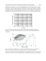
The circuit in the first example is the Miller amplifier in Figure 7. For the sizing tasks the
lengths, widths, and multipliers of the transistors are used as discrete parameters. The lengths
of all transistors shall be equal. Furthermore some multipliers and transistor widths (e.g.,
multipliers and widths of the differential pair) are set equal to avoid mismatch effects. For
transistor lengths and widths a 5nm manufacturing grid is assumed. The Miller capacitance is
represented by a continuous parameter. A 0.5pF load capacitance and a 2V supply voltage are
given for the circuit and the 45nm low power predictive technology (PTM; (Balijepalli et al.,
2007; Cao et al., 2000; Zhao & Cao, 2006)) from (Nanoscale Integration and Modelling Group,
Arizona State University, 2008) is used.
The simulated performance values of the amplifier before and after sizing are shown in Table
1. It can be seen from the results, that – as proposed in Section 1 – the continuous optimization
An SQP and Branch-and-Bound Based Approach for Discrete Sizing of Analog Circuits
311
VDD
w5 ,l1
m5
w6 ,l1
m6
bias
in −
w1 ,l1
m1
w2 ,l1
m2
w7 ,l1
m7
w1 ,l1
m1
w2 ,l1
m2
in +
Cc
out
w8 ,l1
m8
gnd
Fig. 7. Miller Amplifier
Fig. 8. Runtime for up to 8 times parallelized algorithm on a 16 core 2.67GHz computer for
sizing of the Miller amplifier
and subsequent rounding violates two specifications in this case. In contrast, the goal of the
discrete sizing task was achieved if Branch and Bound with or without quadratic model has
been used. The result quality of Branch and Bound with quadratic model is as good as the
result quality achieved without the modification. However, the runtime comparison in Figure
8 clearly shows that the additional runtime for Branch and Bound considering the quadratic
model presented in this paper, is significantly smaller, than without the modification and the
additional cost compared to the optimization with subsequent rounding is neglectable in this
case.
In the second example the sizing of the more complex amplifier in Figure 9, which is
proposed in (Martins, 1998), is shown. For this example the 45nm high performance
predictive technology model from (Nanoscale Integration and Modelling Group, Arizona
State University, 2008) is used and again a 5nm manufacturing grid is assumed. The lengths
of all transistors and the widths of transistors which are in the same current mirror or in the
same differential pair are set equal. Additionally, some multipliers are set equal considering
the symmetries of the circuit. Thus, 14 multipliers, 11 widths, and the length are considered
as discrete parameters. Additionally, the compensation capacitance Cc and the bias voltages
Vbias,1 and Vbias,2 are represented by continuous parameters. A 20pF load capacitance and a 2V
supply voltage are given for the circuit. Again the sizing rules from (Massier & Graeb, 2008)
are used which define 93 constraints in this case. Specifications and simulated performances
312
Advances in Analog Circuitsi
Performance
Specification
Initial
values
SQP
+
Rounding
SQP + BaB
w/o
quadratic
model
SQP + BaB
with
quadratic
model
PSRR
[dB ]
Gain
[dB ]
CMRR
[dB ]
f transit
[ MHz]
> 135
134
138
139
137
> 85
89
89
90
89
> 135
172
167
167
166
> 15
19
24
22
23
61
60
ϕ [◦ ]
> 60
50
59
(violates
spec)
SR (rising)
V
[ μs ]
|SR (falling)|
V
[ μs ]
Area
[( μm )2 ]
>15
10
18
16
17
>15
14
37
31
32
< 10
7
9
9
9
< 50
56
52
(violates
spec)
49
49
Power
[μW ]
Table 1. Specification and performance values for Miller amplifier using 45nm PTM, 2V
supply voltage, 1uA bias current
VDD
l0
w3
m3
l0
w3
m3
l0
w4
m4
l0
w4
m14
Vbias,1
l0
w8
m8
l0
w4
m14
l0
w2
m2
gnd
l0
w1
m1
l0
w5
m13
l0
w7
m7
l0
w10
m10
in −
in +
l0
w5
m5
l0
w4
m4
Vbias,2
l0
w6
m6
l0
w9
m9
l0
w6
m12
l0
w1
m1
Cc
out
l0
w11
m11
l0
w2
m2
l0
w5
m5
l0
w5
m13
l0
w7
m7
Fig. 9. Low-voltage low-power operational amplifier from (Martins, 1998)
An SQP and Branch-and-Bound Based Approach for Discrete Sizing of Analog Circuits
313
Fig. 10. Runtime for up to 8 times parallelized algorithm on a 16 core 2.67GHz computer for
sizing of amplifier in Figure 9
are presented in Tabular 2.
Also in this case specifications are violated when SQP and sub-sequent rounding is used and
also here Branch and Bound with and without quadratic model solves the sizing task. The
runtime comparison in this case shows that also here Branch and Bound using the quadratic
model is much faster than without consideration of the quadratic model. As the number of
discrete parameters is much higher in this case, also the runtime of Branch and Bound on the
quadratic model is relatively large. Thus potential for further improvement of the algorithm
can be seen: The runtime of the algorithm can be reduced if the Branch and Bound algorithm
presented in (3.2) is advanced, which is used to find the discrete optimum on the quadratic
model and needs approximately half of the computational time in this experiment.
The third example shows the sizing process for the sense amplifier from (Yeung & Mahmoodi,
2006) (see Figure 11). Considering the symmetry of the circuit, 5 multipliers, 5 transistor
widths, and the transistor length are used as parameters. For the sizing process a 16nm low
power PTM is used and a 2nm manufacturing grid is assumed. Specifications and results are
listed in Table 3. For the simulation of the delay it is assumed that the inputs (bit line BL and
negative bit line BLB) are preloaded to VDD = 1.5V and the input signal is a voltage reduction
by 10mV at one of them. “Delay +” in Table 3 is defined as the time between the change of the
input signal at the positive input BL and the point of time when the positive output reaches
0.95 · VDD . Accordingly, the value of “Delay −” is defined as the time between the change of
the signal at the negative input BLB and the point of time when the positive output reaches
0.05 · VDD .
The results for this experiment show that in this case continuous optimization with
subsequent rounding leads to a solution of the sizing task. This especially happens, if only
a few or week constraints and specifications are defined and if only a small number of
parameters is used. However, the additional runtime for the modified Branch and Bound
approach is only a few seconds. Further analysis of the results shows, that the additional