Wave Propagation Part 2 potx
Bạn đang xem bản rút gọn của tài liệu. Xem và tải ngay bản đầy đủ của tài liệu tại đây (2.14 MB, 35 trang )
Microwave Sensor Using Metamaterials
27
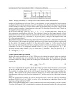
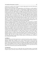
Fig. 16. Transmission coefficient (S21) versus frequency for different dielectric materials in
the detecting zone (Huang et al, 2009)
To quantify the sensitivity of the evanescent mode for dielectric sensing, the performance of
the metamaterial-assisted microwave sensor is compared with the traditional microwave
cavity. We closed both ends of a hollow waveguide with metallic plates, which forms a
conventional microwave cavity (
axbxl=15x7.5x12mm
3
), and computed the resonant
frequency of the cavity located with dielectric sample. Table 1 shows a comparison between
the relative frequency shift, i.e.,
NN1 Nr
ff()f()
Δ
=ε−εof the waveguide filled with coupled
metamaterial particles, and that of the conventional microwave cavity, i.e.,
CC1 Cr
ff()f()Δ= ε− ε. Where,
1
ε
and
r
ε
denotes the relative permittivity of the air and the
dielectric sample, respectively. It indicates that minium (respectively maximum) frequency
shift of the waveguide filled with -shape coupled metamaterial particles is 360 times
(respectively 450 times) that of the conventional microwave cavity. As a consequence, the
waveguide filled with -shape coupled metamaterial particles can be used as a novel
microwave sensor to obtain interesting quantities, such as biological quantities, or for
monitoring chemical process, etc. Sensitivity of the metamaterial-assisted microwave sensor
is much higher than the conventional microwave resonant sensor.
r
1.5 2 2.5 3 3.5 4 4.5 5
f
N
144 288 432 558 684 810 918 1026
f
C
0.4 0.7 1.1 1.3 1.6 1.8 2.2 2.5
f
N
/ f
C
360 411 393 429 428 450 417 410
Table 1. Comparison of the relative frequency shift (MHz) between the waveguide filled
with coupled metamaterial particles and the conventional cavity
In addition, the microwave sensor can also be constructed by filling the other type of
coupled metamaterial particles into the rectangular waveguide. For example, the meander
line and split ring resonator coupled metamaterial particle (Fig. 17(a)); the metallic wire and
split ring resonator (SRR) coupled metamaterial particle (Fig. 17(b)). The red regions shown
in Fig. 17 denote the dielectric substances. Fig. 17(c) and (d) are the front view and the
vertical view of (b).
Wave Propagation
28
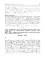
Fig. 17. (a) Configuration of the particle composed of meander line and SRR.
w = 0.15mm, g
= 0.2 mm, p = 2.92 mm, d=0.66mm, c=0.25mm, s=2.8mm, u=0.25mm, and v=0.25mm. (b)
Configuration of the particle composed of metallic wire and SRR. (c) and (d) are the front
view and the vertical view of (b).
l=1.302mm, h=0.114mm, w=0.15mm, d=0.124mm,
D=0.5mm, m=0.5mm
Transmission coefficient of the waveguide filled with any of the above two couple
metamaterial particles also possesses the characteristic of two resonant peaks. When it is
used in dielectric sensing, electromagnetic properties of sample can be obtained by
measuring the resonant frequency of the low-frequency peak, as shown in Fig. 18.
Fig. 18. Transmission coefficient (20log| S21|) versus frequency for a variation of sample
permittivity. (a) The wave guide is filled with coupled meander line and SRR. (b) The wave
guide is filled with coupled metallic wire and SRR. From right to the left, the curves are
corresponding to dielectric sample with permittivity of 1, 1.5, 2, 2.5, 3, 3.5, 4, 4.5, and 5,
respectively
From the above simulation results, we can conclude that the evanescent wave in the
waveguide filled with coupled metamaterial particles can be amplified. The evanescent
mode is red shifted with the increase of sample permittivity. Therefore, the waveguide filled
with couple metamaterial particles can be used as novel microwave sensor. Compared with
the conventional microwave resonant sensor, the metamaterial-assisted microwave sensor
allows for much higher sensitivity.
Microwave Sensor Using Metamaterials
29
5.3 Microwave sensor based on stacked SRRs
Simulation model of the microwave sensor based on stacked SRRs is shown in Fig. 19. The
size of the waveguide is axbxL=22.86x10.16x12.8mm, as shown in Fig. 19(a). Fig.19(b) is the
front view of the SRR with thickness of 0.03mm. It is designed onto a 0.127mm thick substrate
with relative permittivity of 4.6. The geometric parameters for the SRR are chosen as L=1.4mm,
g=s=w=0.3mm, P=2mm, so that the sensor works at the frequency between 8-10.5GHz. Fig.
19(c) is the layout of the stacked SRRs, the distance between two unit cell is U=0.75.
Fig. 19. (a) The microwave sensor based on stacked SRRs. (b) Front view of the SRR cell.
(c) Layout of the stacked SRRs
Firstly, the effective permeability of the stacked SRRs is simulated using the method
proposed by Smith et al (Smith et al, 2005). The simulation results are shown in Fig. 20. It is
seen that the peak value increases with the number of SRR layer, and a stabilization is
achieved when there are more than four SRR layers. Then, in what follows, the microwave
sensor based on stacked SRRs with four layers is discussed in detail.
Fig. 20. Effective permeability of the stacked SRRs. (a) Real part. (b) Imaginary part. From
right to left, the curves correspond to the simulation results of the stacked SRRs with one
layer, two, three, four and five layers
Fig. 21 shows the electric field distribution in the vicinity of the SRR cells. It is seen that the
strongest field amplitude is located in the upper slits of the SRRs, so that these areas become
very sensitive to changes in the dielectric environment. Since the electric field distributions
in the slits of the second and the third SRRs are much stronger than the others, to further
Wave Propagation
30
investigate the potential application of the stacked SRRs in dielectric sensing, thickness of
the SRRs is increased to 0.1mm, and testing samples are located in upper slits the second
and the third SRRs. Simulation results of transmission coefficients for a variation of sample
permittivity are shown in Fig. 22.
Fig. 21. Electric field distribuiton in the vicinity of the four SRRs. (a) The first SRR layer
(x=-0.734 mm). (b) The second SRR layer (x=0.515 mm). (c) The third SRR layer
(x=1.765 mm). (d) The fourth SRR layer (x=3.014 mm)
8.4 8.6 8.8 9
0.3
0.4
0.5
0.6
0.7
0.8
0.9
1
Frequency(GHz)
S21
Fig. 22. Transmission coefficient as a function of frequency for a variation of sample
permittivity. From right to the left, the curves are corresponding to dielectric sample with
permittivity of 1, 1.5, 2, 2.5, 3 and 3.5, respectively
In conclusion, when the stacked SRRs are located in the waveguide, sample permittivity
varies linearly with the frequency shift of the transmission coefficient. Although the periodic
structures of SRRs (Lee et al, 2006; Melik et al, 2009; Papasimakis et al, 2010) have been used
for biosensing and telemetric sensing of surface strains, etc. The above simulation results
demonstrate that the stacked SRRs can also be used in dielectric sensing.
Microwave Sensor Using Metamaterials
31
6. Open resonator using metamaterials
6.1 Open microwave resonator
For the model shown in Fig. 23, suppose the incident electric field is polarized
perpendicular to the plane of incidence, that is,
() ()
=
K
K
ii
y
E
Ee
, then the incident, reflected, and
refracted (transmitted) field can be obtained as
Fig. 23. Snell’s law for
1
0>n and
2
0>n (real line). The dashed line for
1
0>n and
2
0<n
()
0
111
() 2 2 2 1/2
1112 1 12 2
0
2cos /
cos / (1 sin / ) /
φμ
φ
μφμ
=
+−
t
i
E
n
En nn n
(25)
()
22 21/2
0
1112 1 12 2
() 2 2 2 1/2
1112 1 12 2
0
cos / (1 sin / ) /
cos / (1 sin / ) /
φ
μφμ
φ
μφμ
−−
=
+−
r
i
E
nnnn
En nn n
(26)
where
()
0
t
E ,
()
0
r
E and
()
0
i
E are the amplitudes of the transmitted, reflected, and the incident
electric fields, respectively. Provided that
22 2
12 1
(/)sin 1
φ
<
nn , the above formulas are valid for
positive as well as negative index midia. For
22 2
12 1
(/)sin 1
φ
>nn , the expression
22 21/2 22 2 1/2
112 112
(1 sin / ) ( sin / 1)
φφ
−=±−nnjnn. (27)
The
− sign is chosen because the transmitted field must not diverge at infinity for
2
0>n
.
The
+ sign is chosen for
2
0
<
n
. If
1
0>n
and
2
0
<
n
and if
21
ε
ε
=
−
and
21
μ
μ
=−
, then
0
0=
r
E . This means that there is no reflected field. Some interesting scenario shown in Fig.
24 can be envisioned. Fig. 24(a) illustrates the mirror-inverted imaging effect. Due to the
exist of many closed optical paths running across the four interfaces, an open cavity is
formed as shown in Fig. 24(b), although there is no reflecting wall surrounding the cavity.
Fig. 24. (a)Mirror-inverted imaging effect. (b) Formation of an open cavity
Wave Propagation
32
As shown in Fig. 25(a), the open microwave resonator consists of two homogenous
metamaterial squares in air. Its resonating modes are calculated using eigenfrequency
model of the software COMSOL. Fig.25 (b) shows the mode around the frequency of
260MHz. It is in agreement with the even mode reported by He et al. (He et al, 2005). In the
simulation, scattering boundary condition is added to the outer boundary to model the open
resonating cavity. From Fig. 25(b), it is seen that electric field distribution is confined to the
tip point of the two metamaterial squares. Therefore, it will be very sensitive in dielectric
environment. The dependence of resonant frequency on the permittivity of dielectric
environment is shown in Table 2. It is seen that when the permittivity changes from 1 to
1+10
-8
, the variation of resonate frequency is about 14KHz. The variation of resonant
frequency can be easily detected using traditional measuring technique. Therefore, the open
cavity based on metamaterials possesses high sensitivity, and it has potential application for
biosensors.
Fig. 25. (a) A subwavelength open resonator consisting of two homogenous metamaterial
squares in air. (b) The electric field (Ez) distribution for (a)
Frequency(MHz)
260.481 260.467 260.336 259.794 255.372 240.485
Permittivity
1 1+10
-8
1+10
-7
1+5x10
-7
1+10
-6
1+5x10
-6
Table 2. The relation between resonate frequency and environment permittivity
The open resonator using metamaterials was first suggested and analyzed by Notomi
(Notomi, 2000), which is based on the ray theory. Later, He et al. used the FDTD to calculate
resonating modes of the open cavity.
6.2 Microcavity resonator
Fig. 26(a) shows a typical geometry of a microcavity ring resonator (Hagness et al, 1997).
The two tangential straight waveguides serve as evanescent wave input and output
couplers. The coupling efficiency between the waveguides and the ring is controlled by the
size, g, of the air gap, the surrounding medium and the ring outer diameter, d, which affects
the coupling interaction length. The width of WG1, WG2 and microring waveguide is
0.3 m. The straight waveguide support only one symmetric and one antisymmetric mode at
1.5
λ
= m. Fig. 26(b) is the geometry of the microcavity ring when a layer of metamaterials
(the grey region) is added to the outside of the ring. The refractive index of the
metamaterials is n=-1.
Fig. 27 is the visualization of snapshots in time of the FDTD computed field as the pulse first
(t=10fs) couples into the microring cavity and completes one round trip(t=220fs). When
refractive index of the surounding medium varies from 1 to 1.3, the spectra are calculated,
Microwave Sensor Using Metamaterials
33
Fig. 26. (a) The schematic of a microcavity ring resonator coupled to two straight
waveguides. (b) A metamaterial ring (the grey region) is added to the out side of the
microring. d=5.0 m, g=0.23 m, r=0.3 m, the thickness of the metamaterials is r/3
Fig. 27. Visualization of the initial coupling and circulation of the exciting pulse around the
microring cavity resonators
Fig. 28. Spectra for the surrounding medium with different refractive index. (a) Results for
the microring cavity without metamaterial layer. (b)Results for the microring cavity with
metamaterial layer
Wave Propagation
34
as shown in Fig. 28. From Fig. 28(a), it is seen that the resonance peak of the microring cavity
without metamaterial layer is highly dependent on the refractive index of the surrounding
medium, and it is red shifted with the increase of refractive index. From Fig. 28(b) we can
clear observe that the resonance peaks are shifted to the high frequency side when
metamaterial layer is added to the outside of the microring ring resonator. Meanwhile, the
peak value increases with the increase of the refractive index of surrounding medium.
Due to its characteristics of high
Q factor, wide free spectral-range, microcavity can be used
in the field of identification and monitoring of proteins, DNA, peptides, toxin molecules,
and nanoparticle, etc. It has attracted extensive attention world wide, and more details
about microcavity can be found in the original work of Quan and Zhu et al (Quan et al, 2005;
Zhu et al, 2009).
7. Conclusion
It has been demonstrated that the evanescent wave can be amplified by the metamaterials.
This unique property is helpful for enhancing the sensitivity of sensor, and can realize
subwavelength resolution of image and detection beyond diffraction limit. Enhancement of
sensitivity in slab waveguide with TM mode is proved analytically. The phenomenon of
evanescent wave amplification is confirmed in slab waveguide and slab lens. The perfect
imaging properties of planar lens was proved by transmission optics. Microwave sensors
based on the waveguide filled with metamaterial particles are simulated, and their
sensitivity is much higher than traditional microwave sensor. The open microwave
resonator consists of two homogenous metamaterial squares is very sensitive to dielectric
environment. The microcavity ring resonator with metamaterial layer possesses some new
properties.
Metamaterials increases the designing flexibility of sensors, and dramatically improves their
performance. Sensors using metamaterials may hope to fuel the revolution of sensing
technology.
8. Acknowledgement
This work was supported by the National Natural Science Foundation of China (grant no.
60861002), the Research Foundation from Ministry of Education of China (grant no. 208133),
and the Natural Science Foundation of Yunnan Province (grant no.2007F005M).
9. References
Alù, A. & N. Engheta. (2008) Dielectric sensing in -near-zero narrow waveguide channels,”
Phys. Rev. B, Vol. 78, No. 4, 045102, ISSN: 1098-0121
Al-Naib, I. A. I.; Jansen, C. & Koch, M. (2008) Thin-film sensing with planar asymmetric
metamaterial resonators.
Appl. Phys. Lett., Vol. 93, No. 8, 083507, ISSN: 0031-9007
Fedotov, V.A.; Rose, M.; Prosvirnin, S.L.; Papasimakis, N. & Zheludev, N. I. (2007) Sharp
trapped-Mode resonances in planar metamaterials with a broken structural
symmetry.
Phys. Rev. Lett., Vol. 99, No. 14, 147401, ISSN: 1079-7114
Guru, B. S. & Hiziroglu, H. R. (1998). Plane wave propagation, In:
Electromagnetic Field
Theory Fundamentals
, Guru, B. S. & Hiziroglu, H. R. (Ed.), 305-360, Cambridge
University Press, ISBN: 7-111-10622-9, Cambridge, UK, New York
Microwave Sensor Using Metamaterials
35
Huang, M.; Yang, J. J.; Wang, J. Q. & Peng, J. H. (2007). Microwave sensor for measuring the
properties of a liquid drop.
Meas. Sci. Technol., Vol. 18, No. 7, 1934–1938, ISSN:
0957-0233
Huang, M., Yang, J.J., Sun, J., Shi, J.H. & Peng, J.H. (2009) Modelling and analysis of -
shaped double negative material-assisted microwave sensor.
J. Infrared Milli. Terahz.
Waves,
Vol. 30, No. 11, 1131-1138, ISSN: 1866-6892
He, S.; Jin Y.; Ruan, Z. C. & Kuang, J.G. (2005). On subwavelength and open resonators
involving metamaterials of negative refraction index.
New J. Phys., Vol. 7, No. 210,
ISSN: 1367-2630
Hagness, S. C.; Rafizadeh, D.; Ho, S. T. & Taflove, A.(1997). FDTD microcavity simulations:
design and experimental realization of waveguide-coupled single-mode ring and
whispering-gallery-mode disk resonators.
Journal of lightwave Technology, Vol. 15,
No. 11, 2154-2164, ISSN: 0733-8724
Kupfer, K. (2000). Microwave Moisture Sensor Systems and Their Applications, In:
Sensor
Update
, Kupfer, K.; Kraszewski, A. & Knöchel, R, (Ed.), 343-376, WILEY-VCH,
ISBN: 3-527-29821-5, Weinheim (Federal Republic of Germany)
Kraszewski, A. W. (1991). Microwave aquametry-needs and perspectives.
IEEE Trans.
Microwave Theory Tech.,
Vol. 39, No. 5, 828-835, ISSN: 0018-9480
Lee, H. J. & Yook, J. G. (2008). Biosensing using split-ring resonators at microwave regime.
Appl. Phys. Lett., Vol. 92, No. 25, 254103, ISSN: 0003-6951
Marqués, R.; Martel, J.; Mesa, F. & Medina, F. (2002). Left-Handed-Media simulation and
transmission of EM waves in subwavelength split-ring-resonator-loaded metallic
waveguides.
Phys. Rev. Lett., 89, No.18, 183901, ISSN: 0031-9007
Melik, R.; Unal, E.; Perkgoz, N. K.; Puttlitz, C. & Demir, H. V. (2009). Metamaterial-based
wireless strain sensors.
Appl. Phys. Lett., Vol. 95, No. 1, 011106, ISSN: 0003-6951
Notomi, M. (2000). Theory of light propagation in strongly modulated photonic crystals:
Refractionlike behavior in the vicinity of the photonic band gap.
Phys. Rev. B,
Vol.,62, No. 16, 10696-10705, ISSN: 1098-0121
Pendry, J. B. (2000). Negative Refraction Makes a Perfect Lens.
Phys. Rev. Lett., Vol. 85, No.
18, 3966-3969, ISSN: 0031-9007
Papasimakis, Ni.; Luo, Z.Q.; Shen, Z.X.; Angelis, F. D.; Fabrizio, E. D.; Nikolaenko, A. E.; &
Zheludev, N. I. (2010). Graphene in a photonic metamaterial.
Optics Express, Vol.
18, No. 8, 8353-8359, ISSN: 1094-4087
Qing, D. K. & Chen, G. (2004). Enhancement of evanescent waves in waveguides using
metamaterials of negative permittivity and permeability.
Appl. Phys. Lett., Vol. 84,
No. 5, 669-671, ISSN: 0003-6951
Quan, H.Y.; & Guo, Z.X. (2005). Simulation of whispering-gallery-mode resonance shifts for
optical miniature biosensors. Journal of Quantitative Spectroscopy & Radiative
Transfer, Vol. 93, No. 1-3, 231–243, ISSN: 0022-4073
Shelby, R. A.; Smith, D. R. & Schultz, S. (2001). Experimental verification of a negative index
of refraction.
Science, Vol. 292, No. 5514, 77-79, ISSN: 0036-8075
Service, R. F. (2010). Next wave of metamaterials hopes to fuel the revolution.
Science, Vol.
327, No. 5962, 138-139, ISSN: 0036-8075
Wave Propagation
36
Shreiber, D.; Gupta, M. & Cravey, R. (2008). Microwave nondestructive evaluation of
dielectric materials with a metamaterial lens.
Sensors and Actuators, Vol. 144, No.1,
48–55, ISSN
:0924-4247
Silveirinha, M. & Engheta, N. (2006). Tunneling of Electromagnetic Energy through
Subwavelength Channels and Bends using -Near-Zero Materials.
Phys. Rev. Lett.,
Vol. 97, No. 15, 157403, ISSN: 0031-9007
Smith, D. R.; Vier, D C; Koschny, Th. & Soukoulis, C. M. (2005). Electromagnetic parameter
retrieval from inhomogeneous metamaterials.
Phys. Rev. E, Vol. 71, No. 3, 036617,
ISSN: 1539-3755
Taya, S. A.; Shabat, M. M. & Khalil, H. M.(2009). Enhancement of sensitivity in optical
waveguide sensors using left-handed materials.
Optik, Vol. 120, No.10, 504-508,
ISSN: 0030-4026
Von Hippel A, (1995). Dielectric measuring techniques, In:
Dielectric Materials and
Applications,
Hippel A. V., (Ed.) 47-146, Wiley/The Technology Press of MIT, ISBN:
0-89006-805-4, New York
Veselago, V. G. (1968). The electrodynamics of substances with simultaneously negative
values of and .
Sov. Phys. Usp., Vol. 10, No. 4, (1968) 509-514, ISSN: 0038-5670
Wang,W.; Lin, L.; Yang, X. F. Cui, J. H.; Du, C. L. & Luo, X. G. (2008). Design of oblate
cylindrical perfect lens using coordinate transformation.
Optics Express, Vol. 16, No.
11, 8094-8105, ISSN: 1094-4087
Wu, Z.Y.; Huang, M.; Yang J. J.; Peng, J.H. & Zong, R. (2008). Electromagnetic wave
tunnelling and squeezing effects through 3D coaxial waveguide channel filled with
ENZ material,
Proceedings of ISAPE 2008, pp. 752-755, ISBN: 978-1-4244-2192-3,
Kunming, Yunnan, China, Nov. 2008, Institute of Electrical and Electronics
Engineers, Inc., Beijing
Yang J. J.; Huang, M.; Xiao, Z. & Peng, J. H.(2010). Simulation and analysis of asymmetric
metamaterial resonator-assisted microwave sensor.
Mod. Phys. Lett. B, Vol. 24, No.
12, 1207–1215, ISSN: 0217-9849
Zoran, J.; Jakši , O.; Djuric,Z. & Kment, C. (2007). A consideration of the use of
metamaterials for sensing applications:field fluctuations and ultimate performance,
J. Opt. A: Pure Appl., Vol. 9, No. 9, S377–S384, ISSN: 1464-4258
Zhu, J.G.; Ozdemir, S. K.; Xiao, Y. F.; Li, L.; He, L.N. Chen, D.R. & Yang, L.(2009). On-chip
single nanoparticle detection and sizing by mode splitting in an ultrahigh-Q
microresonator.
Nature Photonics, Vol. 4, No.1, 46-49, ISSN: 1749-4885
3
Electromagnetic Waves in
Crystals with Metallized Boundaries
V.I. Alshits
1,2
, V.N. Lyubimov
1
, and A. Radowicz
3
1
A.V. Shubnikov Institute of Crystallography, Russian Academy of Sciences,
Moscow, 119333
2
Polish-Japanese Institute of Information Technology, Warsaw, 02-008
3
Kielce University of Technology, Kielce, 25-314
1
Russia
2,3
Poland
1. Introduction
The metal coating deposited on the surface of a crystal is a screen that locks the
electromagnetic fields in the crystal. Even for a real metal when its complex dielectric
permittivity
ε
m
has large but finite absolute value, electromagnetic waves only slightly
penetrate into such coating. For example, for copper in the wavelength range λ = 10
–5
–10
–3
cm, from the ultraviolet to the infrared, the penetration depth d changes within one order of
magnitude: d ≈ 6 × (10
–8
–10
–7
) cm, remaining negligible compared to the wavelength, d << λ.
In the case of a perfect metallization related to the formal limit
ε
m
→ ∞ the wave penetration
into a coating completely vanishes, d = 0. The absence of accompanying fields in the
adjacent space simplifies considerably the theory of electromagnetic waves in such media. It
turned out that boundary metallization not only simplifies the description, but also changes
significantly wave properties in the medium. For example, it leads to fundamental
prohibition (Furs & Barkovsky, 1999) on the existence of surface electromagnetic waves in
crystals with a positively defined permittivity tensor
ˆ
ε . There is no such prohibition at the
crystal–dielectric boundary (Marchevskii et al., 1984; D’yakonov, 1988; Alshits & Lyubimov,
2002a, 2002b)). On the other hand, localized polaritons may propagate along even perfectly
metalized surface of the crystal when its dielectric tensor
ˆ
ε has strong frequency dispersion
near certain resonant states so that one of its components is negative (Agranovich, 1975;
Agranovich & Mills, 1982; Alshits et al., 2001; Alshits & Lyubimov, 2005). In particular, in
the latter paper clear criteria were established for the existence of polaritons at the metalized
boundary of a uniaxial crystal and compact exact expressions were derived for all their
characteristics, including polarization, localization parameters, and dispersion relations.
In this chapter, we return to the theory of electromagnetic waves in uniaxial crystals with
metallized surfaces. This time we will be concerned with the more common case of a crystal
with a positively defined tensor
ˆ
ε . Certainly, under a perfect metallization there is no
localized eigenmodes in such a medium, but the reflection problem in its various aspects
and such peculiar eigenmodes as the exceptional bulk (nonlocalized) polaritons that transfer
energy parallel to the surface and satisfy the conditions at the metallized boundary remain.
Wave Propagation
38
We will begin with the theory for the reflection of plane waves from an arbitrarily oriented
surface in the plane of incidence of the general position, where the reflection problem is
solved by a three-partial superposition of waves: one incident and two reflected components
belonging to different sheets of the refraction surface. However, one of the reflected waves
may turn out to be localized near the surface. Two-partial reflections, including mode
conversion and “pure” reflection, are also possible under certain conditions. The incident
and reflected waves belong to different sheets of the refraction surface in the former case
and to the same sheet of ordinary or extraordinary waves in the latter case. First, we will
study the existence conditions and properties of pure (simple) reflections. Among the
solutions for pure reflection, we will separate out a subclass in which the passage to the
limit of the eigenmode of exceptional bulk polaritons is possible. Analysis of the
corresponding dispersion equation will allow us to find all of the surface orientations and
propagation directions that permit the existence of ordinary or extraordinary exceptional
bulk waves. Subsequently, we will construct a theory of conversion reflections and find the
configurations of the corresponding pointing surface for optically positive and negative
crystals that specifies the refractive index of reflection for each orientation of the optical axis.
The mentioned theory is related to the idealized condition of perfect metallization and needs
an extension to the case of the metal with a finite electric permittivity
ε
m
. The transition to a
real metal may be considered as a small perturbation of boundary condition. As was
initially suggested by Leontovich (see Landau & Lifshitz, 1993), it may be done in terms of
the so called surface impedance
1
m
ζ / ε= of metal. New important wave features arise in
the medium with
ζ
≠ 0. In particular, a strongly localized wave in the metal (a so-called
plasmon) must now accompany a stationary wave field in the crystal. In a real metal such
plasmon should dissipate energy. Therefore the wave in a crystal even with purely real
tensor
ˆ
ε must also manifest damping. In addition, in this more general situation the
exceptional bulk waves transform to localized modes in some sectors of existence (the non-
existence theorem (Furs & Barkovsky, 1999) does not valid anymore).
We shall consider a reaction of the initial idealized physical picture of the two independent
wave solutions, the exceptional bulk wave and the pure reflection in the other branch, on a
“switching on” the impedance
ζ
combined with a small change of the wave geometry. It is
clear without calculations that generally they should loss their independency. The former
exceptional wave cannot anymore exist as a one-partial eigenmode and should be added by
a couple of partial waves from the other sheet of the refraction surface. But taking into
account that the supposed perturbation is small, this admixture should be expected with
small amplitudes. Thus we arise at the specific reflection when a weak incident wave
excites, apart from the reflected wave of comparable amplitude from the same branch, also a
strong reflected wave from the other polarization branch. The latter strong reflected wave
should propagate at a small angle to the surface being close in its parameters to the initial
exceptional wave in the unperturbed situation.
Below we shall concretize the above consideration to an optically uniaxial crystal with a
surface coated by a normal metal of the impedance
ζ
supposed to be small. The conditions
will be found when the wave reflection from the metallized surface of the crystal is of
resonance character being accompanied by the excitation of a strong polariton-plasmon. The
peak of excitation will be studied in details and the optimized conditions for its observation
will be established. Under certain angles of incidence, a conversion occurs in the resonance
Electromagnetic Waves in Crystals with Metallized Boundaries
39
area: a pumping wave is completely transformed into a surface polariton plasmon of much
higher intensity than the incident wave. In this case, no reflected wave arises: the normal
component of the incident energy flux is completely absorbed in the metal. The conversion
solution represents an eigenmode opposite in its physical sense to customary leaky surface
waves known in optics and acoustics. In contrast to a leaky eigenwave containing a weak
«reflected» partial wave providing a leakage of energy from the surface, here we meet a
pumped surface polariton-plasmon with the weak «incident» partial wave transporting
energy to the interface for the compensation of energy dissipation in the metal.
2. Formulation of the problem and basic relations
Consider a semi-bounded, transparent optically uniaxial crystal with a metallized boundary
and an arbitrarily oriented optical axis. Its dielectric tensor
ˆ
ε is conveniently expressed in
the invariant form (Fedorov, 2004) as
ˆ
ˆ
()
oeo
εεI εε
=
+− ⊗cc, (1)
where
ˆ
I
is the identity matrix, c is a unit vector along the optical axis of the crystal, ⊗ is the
symbol of dyadic product,
ε
o
and
ε
e
are positive components of the electric permittivity of
the crystal. For convenience, we will use the system of units in which these components are
dimensionless (in the SI system, they should be replaced by the ratios
ε
o
/
ε
0
and
ε
e
/
ε
0
, where
ε
0
is the permittivity of vacuum).
In uniaxial crystals, one distinguishes the branches of ordinary (with indices “o”) and
extraordinary (indices “e”) electromagnetic waves. Below, along with the wave vectors
k
α
(
α
= o, e), we shall use dimensionless refraction vectors n
α
= k
α
/k
0
where k
0
=
ω
/c,
ω
is the
wave frequency and c is the light speed. These vectors satisfy the equations (Fedorov, 2004)
ˆ
oo o e e oe
ε , εεε
⋅
=⋅=nn n n . (2)
For real vectors
n
o
and n
e
, the ray velocities (the velocities of energy propagation) of the
corresponding bulk waves are defined by
[]
ˆ
,()()
oe
oe oeeoe
ooeoe
ccε
c
εεε
εεεεε
===+−⋅
nn
uu nncc
. (3)
Formulas (3) show that, in the ordinary wave, energy is transported strictly along the
refraction vector, whereas, in the extraordinary wave, generally not.
For our purposes, it is convenient to carry out the description in a coordinate system
associated not with the crystal symmetry elements, but with the wave field parameters. Let
us choose the x axis in the propagation direction
m and the y axis along the inner normal n
to the surface. In this case, the xy plane is the plane of incidence where all wave vectors of
the incident and reflected waves lie, the xz plane coincides with the crystal boundary, and
the optical axis is specified by an arbitrarily directed unit vector
c (Fig. 1). The orientation of
vector
c = (c
1
, c
2
, c
3
) in the chosen coordinate system can be specified by two angles, θ and φ.
The angle θ defines the surface orientation and the angle φ on the surface defines the
propagation direction of a stationary wave field.
Wave Propagation
40
Metal
coating
y
n
c
m
x
z
θ
Interface
surface
Incidence
plane
Optical
axis
c
1
c
3
c
2
φ
Fig. 1. The system of xyz coordinates and the orientation
c of the crystal’s optical axis
The stationary wave field under study can be expressed in the form:
(,,) ()
exp[ )]
(,,) ()
xyt y
ik(x vt
xyt y
⎛⎞⎛⎞
=−
⎜⎟⎜⎟
⎝⎠⎝⎠
EE
HH
. (4)
The y dependence of this wave field is composed from a set of components. In the crystal (y
> 0) there are four partial waves subdivided into incident (i) and reflected (r) ones from two
branches, ordinary (o) and extraordinary (e):
() () () () ()
()
() () () ()
irir
ooee
irir
ooee
irir
ooee
yyyyy
CCCC
y
yyyy
⎛⎞⎛⎞⎛⎞⎛⎞
⎛⎞
⎜⎟⎜⎟⎜⎟⎜⎟
=+++
⎜⎟
⎜⎟⎜⎟⎜⎟⎜⎟
⎝⎠
⎝⎠⎝⎠⎝⎠⎝⎠
EE E E E
H
HHHH
. (5)
Here the vector amplitudes are defined by
()
exp( )
()
i,r i,r
oo
o
i,r i,r
oo
y
i
p
k
y
y
⎛⎞⎛⎞
⎜⎟⎜⎟
=
⎜⎟⎜⎟
⎝⎠⎝⎠
Ee
Hh
∓ , (6)
⎛⎞⎛⎞
⎜⎟⎜⎟
=
⎜⎟⎜⎟
⎝⎠⎝⎠
∓
()
exp[ ( ) ]
()
i,r i,r
ee
e
i,r i,r
ee
y
i
pp
k
y
y
Ee
Hh
. (7)
In Eqs. (4)–(7),
E, e and H, h are the electric and magnetic field strengths, k is the common x
component of the wave vectors for the ordinary and extraordinary partial waves: k =
i,r i,r
oe
⋅= ⋅kmkm, v = ω/k is the tracing phase velocity of the wave, and
i,r
o
C and
i,r
e
C are the
amplitude factors to be determined from the boundary conditions. The upper and lower
signs in the terms correspond to the incident and reflected waves, respectively.
In the isotropic metal coating (
y < 0) only two partial waves propagate differing from each
other by their
TM and TE polarizations:
exp
TM TE
mm
TM TE
mm m
TM TE
mm
(y)
CC (ikpy)
(y)
⎛⎞
⎛⎞ ⎛⎞
⎛⎞
⎜⎟
⎜⎟ ⎜⎟
=+ −
⎜⎟
⎜⎟ ⎜⎟
⎜⎟
⎝⎠
⎝⎠ ⎝⎠
⎝⎠
Eee
H
hh
. (8)
By definition, the above polarization vectors are chosen so that the
TM wave has the
magnetic component orthogonal to the sagittal plane and the electric field is polarized in
Electromagnetic Waves in Crystals with Metallized Boundaries
41
this plane, and for the TE wave, vice versa, the magnetic field is polarized in-plane and the
electric field – out-plane:
||(0, 0, 1)
TM
m
h , ||
TM TM
mmm
×enh, ||(0, 0, 1)
TE
m
e , ||
TE TE
mmm
×hne. 9)
The refraction vectors of the partial waves in the superpositions (5) and (8) are equal
(1, , 0)
i,r T
oo
np=n ∓ , (1, , 0)
i,r T
ee
npp=n ∓ , (1, , 0)
T
mm
np=−n . (10)
Here, the superscript T stands for transposition and n = k/k
0
= c/v is the dimensionless wave
slowness also called the refractive index. The parameters p
o
, p
e
, p and p
m
that determine the
dependences of the partial amplitudes on depth y can be represented as
1
o
ps
=
− ,
e
γ
B
ps
AA
⎛⎞
=−
⎜⎟
⎝⎠
,
12
(1 )
cc
p γ
A
=−
,
m
R
p
n
ζ
= , (11)
where we use the notation
2
o
s ε /n=
,
eo
γε/ ε
=
,
2
2
1(1)Acγ
=
+−
,
2
3
1(11/)Bc
γ
=− −
,
2
1-( )Rn
ζ
= . (12)
The orientation of the polarization vectors in (5), (6) is known from (Born & Wolf, 1986;
Landau & Lifshitz, 1993) and can be specified by the relations
,,,
i,r i,r i,r i,r i,r i,r i,r i,r
oo eee o
ααα
α o,e×⋅−=×=e ||n c e ||n (n c) ε chne . (13)
Substituting relations (10) into (9) and (13) one obtains
332 1
12 2 13
(, , )
[( ), ]
i,r T
ooo
i,r
o
i,r T
o
oo o
pc c c pc
N
-n
pp
cc c
p
c, cs±
⎛⎞⎛⎞
−±
⎜⎟⎜⎟
=
⎜⎟
⎜⎟
±
⎝⎠ ⎝ ⎠
e
h
∓
, (14)
11 2 21 2 3
332 1
{[()]/,[()]()/,}
[( ) , , ( ) ]
i,r T
eeee
i,r
e
i,r T
e
ee
c c ppc sc c ppc pp s c
N
np pc c c p pc
⎛⎞⎛⎞
−+ −+
⎜⎟⎜⎟
=
⎜⎟
⎜⎟
−−
⎝⎠ ⎝ ⎠
e
h
∓∓∓
∓∓
, (15)
(, , 0)
(0, 0, 1)
TM T
m
TM T
m
Rn
ζζ
⎛⎞⎛⎞
⎜⎟⎜⎟
=
⎜⎟
⎜⎟
⎝⎠⎝ ⎠
e
h
,
(0, 0 )
(, , 0)
TE T
m
TE T
m
, -
Rn
ζ
ζ
⎛⎞⎛⎞
⎜⎟⎜⎟
=
⎜⎟
⎜⎟
⎝⎠⎝ ⎠
e
h
. (16)
The normalization in (14)-(16) was done from the conditions
||1
o,e
i,r
=
h and | | 1
m
α
=h . It
already presents in (16) and the factors N
o,e
in (14), (15) are specified by the equations
22
21 3
1/ [( ) ]
i,r
oo o
N ε cc
p
cs=±+,
22
12
1/ 1 ( ) [ ( )]
i,r
ee e
Nn pp ccpp=+ −+∓∓. (17)
3. Boundary conditions and a reflection problem in general statement
The stationary wave field (4) at the interface should satisfy the standard continuity
conditions for the tangential components of the fields (Landau & Lifshitz, 1993):
Wave Propagation
42
00 0 0
||,| |
ty ty ty ty
=
+=− =+ =−
=
=EE HH. (18)
When the crystal is coated with perfectly conducting metal, the electric field in the metal
vanishes and the boundary conditions (18) reduces to
0
|0
ty=+
=
E . (19)
When the perfectly conducting coating is replaced by normal metal with sufficiently small
impedance
ζζ iζ
′
′′
=+
(
0ζ
′
>
,
0ζ
′
′
<
), it is convenient to apply more general (although also
approximate) Leontovich boundary condition (Landau & Lifshitz, 1993) instead of (19):
0
()0
tty
ζ
=+
+
×=EHn . (20)
Below in our considerations, the both approximations, (19) and (20), will be applied.
However we shall start from the exact boundary condition (18).
3.1 Generalization of the Leontovich approximation
The conditions (18) after substitution there equations (5)-(8) and (16) take the explicit form
0
0
0
10
rr r i i
ox ex o ox ex
rr r i i
oz ez e oz ez
ii
oe
rr TM i i
ox ex m ox ex
rr TE i i
oz ez m oz ez
ee R C e e
ee - C e e
CC
hh RC h h
hh C h h
ζ
ζ
⎛⎞⎛⎞⎛⎞⎛⎞
⎜⎟⎜⎟⎜⎟⎜⎟
⎜⎟⎜⎟⎜⎟⎜⎟
=− −
⎜⎟⎜⎟⎜⎟⎜⎟
⎜⎟⎜⎟⎜⎟⎜⎟
⎜⎟⎜⎟⎜⎟⎜⎟
⎝⎠⎝⎠⎝⎠⎝⎠
. (21)
Following to (Alshits & Lyubimov, 2009a) let us transform this system for obtaining an exact
alternative to the Leontovich approximation (20). We eliminate the amplitudes
TM
m
C and
TE
m
C
of the plasmon in metal from system (21) and reduce it to the system of two equations:
0
// //
rr r r r ii i i i
ox ex oz ez o ox ex oz ez o
rr r r r ii i i i
oz ez ox ex e oz ez ox ex e
e e -Rh -Rh C e e -Rh -Rh C
ee hRhRC ee hRhRC
ζζ
⎡⎤⎡⎤
⎛⎞⎛⎞⎛⎞⎛⎞⎛⎞⎛⎞
⎢⎥⎢⎥
⎜⎟⎜⎟⎜⎟⎜⎟⎜⎟⎜⎟
+++=
⎜⎟⎜⎟⎜⎟⎜⎟⎜⎟⎜⎟
⎢⎥⎢⎥
⎝⎠⎝⎠⎝⎠⎝⎠⎝⎠⎝⎠
⎣⎦⎣⎦
. (22)
Taking into account the matrix identities
(1 )
// //
i,r i,r i,r i,r i,r i,r
oz ez oz ez oz ez
i,r i,r i,r i,r i,r i,r
ox ex ox ex ox ex
-Rh -Rh -h -h h h
R
hRhR h h hRhR
⎛⎞⎛⎞⎛⎞
⎜⎟⎜⎟⎜⎟
=+−
⎜⎟⎜⎟⎜⎟
⎝⎠⎝⎠⎝⎠
(23)
and the explicit form of two-dimensional vectors
E
t
= (E
tx
, E
tz
)
T
and H
t
= (H
tx
, H
tz
)
T
residing
in the xz plane, namely
irir
ox ox ex ex
irir
to o e e
irir
oz oz ez ez
eeee
CCCC
eeee
⎛⎞ ⎛⎞ ⎛⎞ ⎛⎞
⎜⎟ ⎜⎟ ⎜⎟ ⎜⎟
=+++
⎜⎟ ⎜⎟ ⎜⎟ ⎜⎟
⎝⎠ ⎝⎠ ⎝⎠ ⎝⎠
E , (24)
irir
ox ox ex ex
irir
to o e e
irir
oz oz ez ez
hhhh
CCCC
hhhh
⎛⎞ ⎛⎞ ⎛⎞ ⎛⎞
⎜⎟ ⎜⎟ ⎜⎟ ⎜⎟
=+++
⎜⎟ ⎜⎟ ⎜⎟ ⎜⎟
⎝⎠ ⎝⎠ ⎝⎠ ⎝⎠
H , (25)
Electromagnetic Waves in Crystals with Metallized Boundaries
43
system (22) reduces to the following equation
0
ˆ
{(1)}0
tt ty
ζζRN
=+
+
×+ − =EHn H , (26)
where the function R(ζn) was defined in (12), and
ˆ
()N ζn
is the 2 × 2 matrix:
01
ˆ
()
1/ ( ) 0
N ζn
R ζn
⎛⎞
=
⎜⎟
⎝⎠
. (27)
Notice that equation (26) is equivalent to an initial set of conditions (18). Impedance
ζ
in Eq.
(26) is not assumed to be small and this expression only includes crystal fields (5)-(7). Thus,
equation (26) is the natural generalization of Leontovich boundary condition (18).
However, the impedance
ζ
of ordinary metals (like copper or aluminum) may be considered
as a small parameter, especially in the infrared range of wavelengths. In this case, function
R(
ζ
n) in equation (26) [see in (12)] can be expanded in powers of the small parameter (
ζ
n)
2
,
holding an arbitrary number of terms and calculating the characteristics of the wave fields
with any desired precision. This expansion comprises odd powers of the parameter
ζ
:
32 2
121
1
1(21)!!
ˆˆ
(0
2
2( 1)!
s
tt st
s
s
s
ζζnN ζ)N
s
∞
+
=
⎛⎞
−
+
×+ + =
∑
⎜⎟
⎜⎟
+
⎝⎠
EHn H
, (28)
where the set of matrices
ˆ
m
N
(m = 2s + 1) is defined by the expression
01
ˆ
0
m
N
m
⎛⎞
=
⎜⎟
⎝⎠
. (29)
In view of our considerations, from expansion (28) it follows that the discrepancy between
Leontovich approximation (20) and the exact boundary condition starts from the cubic term
~ζ
3
; hence the quadratic corrections ~ζ
2
to the wave fields are correct in this approach.
3.2 Exact solution of the reflection problem
Now let us return to the reflection problem, i.e. to the system (21), which, together with
relations (14) and (15), determines the amplitudes of superpositions (5) and (8). The right-
hand side of (21) is considered to be known. When the reflection problem is formulated,
only one incident wave is commonly considered by assuming its amplitude to be known
(while the other is set equal to zero). The refractive index n, which directly determines the
angle of incidence, is also assumed to be known, while the amplitudes of the reflected waves
in the crystal and those of the plasmon components in the metal are to be determined.
Being here interested only in wave fields in the crystal, we can start our analysis from the
more simple system (22) of only two equations with two unknown quantities. Omitting
bulky but straightforward calculations we just present their results in the form of the
reflection coefficients for the cases of an ordinary incident wave,
i
rri
oe o
oeeoo
oo eo
irir
ooeo ooee
D( p ,p )N
CCDN
r,r
CD(
p
,
p
)N C D(
p
,
p
)N
−
==− ==− , (30)
and an extraordinary incident wave,
Wave Propagation
44
i
rri
oee
eooee
ee oe
irir
eoee eoeo
D(p , p )N
CCDN
r,r
CD(
p
,
p
)N C D(
p
,
p
)N
−
==− ==− . (31)
In the above equations the following notation is introduced
2
12 1 2 21
2
3
( )(1 / ){ ( ) [ ( )]}
()[1()/],
oe o o o e e
oe
D(p ,p ) c p c p ζnRcp cpp ζnRs c c p p
csp ζnRs p p ζnR
=−+ −+− −+
++ ++
(32)
2
321
2(1-)( /)
eo o o
Dcps ζ ccζnR
ε
=+, (33)
2
321
2(1- )( /)
oe e o
Dcp ζ ccζnR
ε
=−. (34)
One can check that these expressions fit the known general equations (Fedorov & Filippov,
1976). Before beginning our analysis of Eqs. (30)-(34), recall that we consider only the
crystals (and frequencies) that correspond to a positively defined permittivity tensor (ε
o
> 0
and ε
e
> 0). Depending on the relation between the components ε
o
and ε
e
, it is customary to
distinguish the optically positive (ε
e
> ε
o
, i.e., γ > 1) and optically negative (ε
e
< ε
o
, i.e., γ < 1)
crystals. Figure 2 shows the sections of the sheets of the refraction surface for these two
types of crystals by the xy plane of incidence for arbitrary orientation of the boundary and
propagation direction. Among the main reflection parameters shown in Fig. 2, the limiting
values of the refractive indices
o
n
ˆ
and
e
n
ˆ
play a particularly important role:
ˆ
oo
n ε= ,
ˆ
eo
n ε A/B= . (35)
These separate the regions of real and imaginary values of the parameters p
o
and p
e
:
2
ˆ
(/) 1
oo
pnn=
−
,
22
ˆ
[( / ) 1] /
ee
pnn
γ
BA= − . (36)
Fig. 2. Sections of the ordinary and extraordinary sheets of the refraction surface by the xy
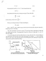
plane of incidence and main parameters of the reflection problem for optically positive (a)
and optically negative (b) crystals
p
e
n
n
e
n
ˆ
o
n
ˆ
i
o
n
r
e
n
r
o
n
p
o
n
i
e
n
pn
p
e
n
y
x
(b)
p
e
n
n
i
e
n
i
o
n
r
e
n
pn
p
e
n
n
o
n
ˆ
e
n
ˆ
p
o
n
y
x
(a)
β
o
e
α
Electromagnetic Waves in Crystals with Metallized Boundaries
45
The parameter p
o
remains real only in the region 0 ≤ n ≤ n
ˆ
o
, i.e., as long as the vertical
straight line in Fig. 2 crosses the corresponding circular section of the spherical refraction
sheet for ordinary waves (or touches it). Similarly, the parameter p
e
remains real only in the
region 0 ≤ n ≤ n
ˆ
e
. In both regions of real values, the refractive index n = 0 describes the
reflection at normal incidence.
Thus, when the stationary wave motions along the surface are described, three regions of
the refractive index n should be distinguished:
(I) 0 < n ≤ min{
ˆ
o
n ,
ˆ
e
n }, (II) min{
ˆ
o
n ,
ˆ
e
n } < n ≤ max{
ˆ
o
n ,
ˆ
e
n }, (III) n > max{
ˆ
o
n ,
ˆ
e
n }. (37)
In the first region, both p
o
and p
e
are real — this is the region of reflections where all partial
waves are bulk ones. This situation automatically arises in an optically positive crystal with
an ordinary incident wave (Fig. 2a) or in an optically negative crystal with an extraordinary
incident wave (Fig. 2b).
In region II, one of the parameters, p
o
or p
e
, is imaginary. This is p
o
in an optically positive
crystal and p
e
in an optically negative one. Therefore, in the general solutions found below,
one of the partial “reflected” waves may turn out to be localized near the surface. In
particular, in this region, the amplitudes
r
e
C
(30) and
r
o
C
(31), respectively, in optically
negative and positive crystals describe precisely these localized reflection components.
Finally, in region III, both parameters,
p
o
and p
e
, are imaginary. In other words, in this
region, a stationary wave field is possible in principle only in the form of surface
electromagnetic eigenmodes — polaritons at fixed refractive index
n specified by the poles
of solutions (30) and (31), i.e., by the equation
D(n) = 0. (38)
In this paper devoted mainly to the theory of reflection, only regions I and II (37) can be of
interest to us. In principle, Eqs. (30) and (31) completely solve the reflection problem. In
contrast to the problem of searching for eigenmodes, where the dispersion equation (38)
specifying the admissible refractive indices
n should be analyzed, the choice of n in the case
of reflection only fixes the angle of incidence of the wave on the surface. In this case, the
crystal cannot but react to the incident wave, while Eqs. (30) and (31) describe this reaction.
However, the reflection has peculiar and sometimes qualitatively nontrivial features for
certain angles of incidence. For example, the three-partial solution can degenerate into a
two-partial one, so only one reflected wave belonging either to the same sheet of the
refraction surface (simple reflection) or to the other sheet (mode conversion) remains instead
of the two reflected waves. At the same time, when grazing incidence is approached, the
total wave field either tends to zero or remains finite, forming a bulk polariton. Below, we
will consider the mentioned features in more detail for the particular case of perfect
metallization (
ζ
= 0) when explicit analysis give visible results.
4. Specific features of wave reflection from the perfectly metallized boundary
The found above general expressions for reflection coefficients (30), (31) remain valid if to
put into (32)-(34)
ζ
= 0 and R = 1. As a result, we come to the much more compact functions
22
1212 3
(, )( )( )
oe o e oo
Dp p cp c cg cp cpε /n=− −+ , (39)
Wave Propagation
46
2
23
2
eo o o
Dccpε /n= , (40)
23
2
oe e
Dccp= , (41)
where the new function
()gn is introduced
2
22
3
2
22
1
1
() ( 1)
o
oe
ε c
cA
gn ppp γ
Acγ
nA
⎛⎞
=−=− = − −
⎜⎟
⎜⎟
⎝⎠
. (42)
With these simplifications we can proceed with our analysis basing on (Alshits et al., 2007).
4.1 Simple reflection
Let us consider the first type of two-partial reflections known as a pure (or simple)
reflection. In this case the incident and reflected waves belong to the same refraction sheet,
i.e., both components are either ordinary or extraordinary. It is obvious that such reflections
take place when the amplitudes
r
e
C in (30) or
r
o
C in (31) become zero. This occurs when D
oe
(40) or D
eo
(41) vanishes, respectively. It is easily seen that both types of pure reflections are
defined by the same criterion:
c
2
c
3
= 0. (43)
As follows from Eq. (43), the pure reflections of both ordinary and extraordinary waves in
the crystals under consideration should exist independently of one another in the same two
reflection geometries. This takes place only in those cases where the optical axis belongs
either to the crystal surface (
c
2
= 0) or to the plane of incidence (c
3
= 0). Since the optical axis
in this case has a free orientation in these planes and since the angle of incidence is not
limited by anything either, the pure reflections in three-dimensional space {
n, c} occupy the
surfaces defined as the set of two planes:
c
2
= 0 and c
3
= 0. Let us consider in more detail the
characteristics of pure reflections in these two geometries.
4.1.1 The optical axis parallel to the surface
In this case, c
2
= 0, i.e., θ = 0, and the xy plane of incidence perpendicular to the surface
makes an arbitrary angle
φ with the direction of the optical axis. The main parameters for
the independent reflections of ordinary and extraordinary waves take the form
{1 ( ) 0}
i,r T
o,e o,e
n, p n,=n ∓ ; (44)
331
22
113
()
()
i,r T
ooo
i,r T
oooo
cp,c, cp
ncp , cp , cε /n
⎛⎞⎛ ⎞
±
⎜⎟⎜ ⎟
=
⎜⎟⎜ ⎟
±
⎝⎠⎝ ⎠
e
h
∓
,
22
113
331
()
()
i,r T
eoeo o
i,r T
eee
cp , cp,cε /n n/ε
cp, c, cp
⎛⎞⎛ ⎞
±
⎜⎟⎜ ⎟
=
⎜⎟⎜ ⎟
−±
⎝⎠⎝ ⎠
e
h ∓
; (45)
ri
oo
CC=
,
ri
ee
CC
=
−
. (46)
As above, the upper and lower signs in Eqs. (44) and (45) correspond to the incident (
i) and
reflected (
r) waves, respectively. In Eq. (11) for p
e
(n), we should take into account the fact
that
A = 1 and B =
2
1
c +
2
3
c /γ in this case. The angles of incidence are defined by n <
ˆ
o,e
n . For
brevity, the normalizing factors in Eqs. (45) are included in the amplitudes
i,r
o,e
C .
Electromagnetic Waves in Crystals with Metallized Boundaries
47
Given (44)–(46), the pure reflection of the electric component of an ordinary wave in this
geometry can be described by the combination
(
)
( ) exp( ) exp( exp[ ( )]
ir
oooooo
x,y,t C ip ky ip ky ik x vt=−+ −Ee e
. (47)
And the pure reflection of the magnetic component of an extraordinary wave is specified by
a similar superposition:
(
)
=−− −( ) exp( ) exp( exp[ ( )].
ir
eeeeee
x,y,t C ip ky ip ky ik x vtHe e
(48)
4.1.2 The optical axis parallel to the plane of incidence
In this case, c
3
= 0, i.e., the azimuth φ = 0, while the angle θ is arbitrary, which corresponds
to arbitrarily oriented crystal surface and plane of incidence passing through the optical
axis. The main parameters of the independently reflected waves are given by the formulas
{1, ( ) 0}
i,r T
oo
npn,=n ∓ , {1, ( ), 0}
i,r T
ee
nppn=n ∓ ; (49)
,
,
(0,0,1)
(,1,0)
ir T
o
ir T
oo
e
hnp
⎛⎞⎛ ⎞
⎜⎟⎜ ⎟
=
⎜⎟⎜ ⎟
−
⎝⎠⎝ ⎠
∓
,
(,0)
(0,0,1)
i,r 2 T
ee e
i,r T
ee
p,γ /A pp
ε /An
⎛⎞⎛ ⎞
±±
⎜⎟⎜ ⎟
=
⎜⎟⎜ ⎟
⎝⎠⎝ ⎠
e
h
; (50)
ri
oo
CC
=
− ,
ri
ee
CC
=
. (51)
At
c
3
= 0 in Eq. (11) for p
e
(n), we have B = 1 and A =
2
1
c +γ
2
2
c . Thus, according to Eqs. (50), the
pure reflection of ordinary waves is described by the partial
TE modes with the electric
component orthogonal to the sagittal plane. Similarly, the partial components of the pure
reflection of extraordinary waves are formed by the
TM modes with the magnetic
component perpendicular to the same plane. In the case under consideration, the analogues
of Eqs. (47) and (48) are even simpler:
( ) (0,0,1)sin( )exp[ ( )]
oo o
x,y,t C p ky ik x vt
=
−E , (52)
( ) (0, 0, 1)cos( )exp[ ( )]
ee e
x,y,t C p ky ik x py vt=+−H
. (53)
4.2 Exceptional bulk polaritons
4.2.1 Simple reflections of ordinary waves at grazing incidence
As we see from Fig. 2, the grazing incidence of an ordinary wave is realized at n =
o
n
ˆ
, when,
according to Eq. (36),
p
o
= 0. In this case, the simple reflection of an ordinary wave in the c
2
=
0 and
c
3
= 0 planes behaves differently as grazing incidence is approached, p
o
→ 0. As
follows from Eqs. (44)–(46), in the former case where the optical axis is parallel to the surface
(
c
2
= 0), the incident and reflected partial waves at p
o
= 0 are in phase and together form an
ordinary exceptional bulk wave:
()
ˆ
exp ( )
()
o
oo
o
x,t
ω
Cinxct
x,t
c
⎛⎞⎛⎞
⎛⎞
=−
⎜⎟⎜⎟
⎜⎟
⎝⎠
⎝⎠⎝⎠
Ee
Hh
. (54)
Wave Propagation
48
The refraction vector of the wave under consideration and its vector amplitude are
ˆˆ
(1, 0, 0) , ε
oooo
nn==n ,
(0, 1, 0)
ˆ
(0, 0, 1)
o
o
o
n
⎛⎞
⎛⎞
⎜⎟
=
⎜⎟
⎜⎟
⎝⎠
⎝⎠
e
h
, (55)
and the energy flux (Poynting vector) in this wave,
P
o
= E
o
× H
o
, lies at the intersection of the
crystal surface with the sagittal surface, i.e.,
P
o
|| x (Fig. 3a).
Fig. 3.
Characteristics of the ordinary (a) and extraordinary (b) bulk polaritons that emerge
at
c
2
= 0 and c
3
= 0, respectively
On the other hand, the pure reflection of ordinary waves in the sagittal plane parallel to the
optical axis (
c
3
= 0, c
2
≠ 0) as grazing incidence is approached (p
o
→ 0), according to Eqs. (52),
gives antiphase incident and reflected partial waves that are mutually annihilated. In other
words, no exceptional bulk polariton emerges on the branch of ordinary waves in this plane.
The qualitative difference in the behavior of grazing incidence in the
c
2
= 0 and c
3
= 0 planes
that we found has a simple physical interpretation. For the limiting wave arising at grazing
incidence to exist, its polarization
E
o
, according to the boundary condition (19), must be
orthogonal to the crystal surface,
E
o
|| n || y. As we see from Eqs. (45), this is actually the
case for an ordinary wave at
c
2
= 0 and as p
o
→ 0. However, the incident and reflected
components in the sagittal plane, according to Eqs. (50) and (52), give polarization
E
o
that is
not orthogonal, but parallel to the surface; hence the annihilation of these components.
4.2.2 Simple reflections of extraordinary waves at grazing incidence
The grazing incidence of extraordinary waves is considered similarly. It relates to n→
ˆ
e
n and
by (36), to
p
e
→ 0. In this case, the reverse is true: the incident and reflected waves are in
antiphase (46) and, hence, are annihilated in the
c
2
= 0 plane, and being in phase (51) when
the optical axis is parallel to the sagittal (
c
3
= 0) plane, which generates a bulk polariton:
0
()
ˆ
exp [ ( ) ]
()
e
ee
e
x,y,t
ω
Cinxpyct
x,y,t
c
⎛⎞⎛⎞
⎛⎞
=+−
⎜⎟⎜⎟
⎜⎟
⎝⎠
⎝⎠⎝⎠
Ee
Hh
, (56)
where
0
ˆ
e
n is
ˆ
e
n taken at c
3
= 0 and p
e
= 0. For the wave under consideration, we have
0
0
(0, 1, 0)
ˆ
(1, , 0) ,
ˆ
(0, 0, 1)
e
ee
e
e
pn
n
⎛⎞
⎛⎞
==
⎜⎟
⎜⎟
⎜⎟
⎝⎠
⎝⎠
e
n
h
, (57)
x
o
n
ˆ
y
P
o
o
n
ˆ
(a)
e
np
ˆˆ
P
e
e
n
ˆ
y
e
n
ˆ
x
(b)
Electromagnetic Waves in Crystals with Metallized Boundaries
49
022 02
12 12
ˆˆ
()()
eo oe oe e
n ε A ε c ε c,p εεcc / n==+ =−
. (58)
As we see from Eq. (57), the bulk polariton (56) is actually polarized in accordance with
requirement (19):
e
e
|| n. Note that the refraction vector n
e
(57) is generally not parallel to
the surface. But the Poynting vector of the wave
P
e
still lies at the intersection of the sagittal
plane and the crystal surface,
P
e
|| x (Fig. 3b). One can show that this is a general property
of exceptional waves for
ζ
= 0 holding even in biaxial crystals (Alshits & Lyubimov, 2009b).
In the special case of
c
2
= c
3
= 0, which corresponds to the propagation direction x along the
optical axis, the sheets of the ordinary and extraordinary waves of the refraction surface are
in contact. As a result, degeneracy arises:
0
oe
ppp
=
==,
ˆˆ
oe o
nn ε== , (1, 0, 0)
oe
==nn , (59)
and solutions (54) and (56) merge, degenerating into the corresponding
TM wave. Since the
uniaxial crystal in the case under consideration is transversally isotropic, the orientation of
the
xy coordinate plane is chosen arbitrarily: for any fixed boundary parallel to the optical
axis, a bulk wave with a polarization vector
E
c
orthogonal to the surface and an energy flux
P
c
|| x can always propagate along the latter.
4.2.3 Proving the absence of other solutions
Thus, exceptional ordinary bulk polaritons (54) emerge when the optical axis is parallel to the
crystal surface. At the same time, similar
extraordinary eigenmodes (56) exist if the optical
axis is parallel to the sagittal plane. In both cases,
TM-type one-partial solutions with an
energy flux
P
o, e
parallel to both the crystal surface and the sagittal plane occur (Fig. 3).
Let us show that the dispersion equation (38), (39),
22
1212 3
()( )(1)0
oeoo
Dcpccgcp cpp
=
−−+ += (60)
has no other eigensolutions. In principle, an exceptional bulk polariton does not need to
belong to the family of simple reflections. It could also be a two-partial one, i.e., consist of
the bulk component of one branch corresponding to outer refraction sheet and the admixing
localized component of the other branch. Examples of such mixed solutions are known both
for crystals with a metallized surface [in the special case of ε
o
= 0 and ε
e
> 0 (Alshits &
Lyubimov, 2005)] and at the open boundary of a crystal with a positively defined tensor
ˆ
ε
(Alshits & Lyubimov, 2002a and 2002b). However, it is clear that any such wave with or
without an admixture of inhomogeneous components carries energy parallel to the surface,
i.e., its bulk component should have a zero parameter
p
o
or p
e
(Fig. 3).
Substituting into (60) Eqs. (11) and (42) for
p
e
and g taken at p
o
= 0,
21 2
()0
e
ccgcp
−
= , (61)
it is easy to see that at
γ < 1 the parameter g is real, while the parameter p
e
is imaginary and,
apart from the already known solution
c
2
= 0, Eq. (60) has no other solutions, since the
localization parameter
p
e
(11) does not become zero at c
2
≠ 0. At γ > 1, when p
e
is also real,
Eq. (60) is equivalent to the requirement
22 2
22 3
()0cc c
+
= , (62)
Wave Propagation
50
which again leads to the solution
2
c = 0.
At
p
e
= 0, Eq. (60) takes the form
2
312
[1)]0
o
cAp (γ cc
+
−=, (63)
where it is considered that
p
e
= 0 at n =
ˆ
e
n and, according to Eqs. (35) and (36),
22
23
(1 )( )
o
p γ cc/γ /A=− +
. (64)
This time the complexity in the dispersion equation (63) arises at
γ > 1; the purely imaginary
parameter
p
o
at c
3
≠ 0 does not become zero, so c
3
= 0 is the only root of Eq. (63). At γ < 1, it is
convenient to rewrite Eq. (63) as
222 22
32 2
{[1(1)]}0c γ c γ c
+
−− =. (65)
Since the expression in braces is positive at any direction of the optical axis,
c
3
= 0 again
remains the only root of the dispersion equation.
Thus, there are no new solutions for exceptional bulk polaritons other than the one-partial
eigenmodes (54) and (56) in crystals with a perfectly metallized boundary found above.
4.3 Mode conversion at reflection
Let us now turn to the other, less common type of two-partial reflections where the wave
incident on the surface is converted into the reflected wave of the “conjugate” polarization
branch (i.e., belonging to the other refraction sheet). We pose the following question: Under
what conditions does the mode conversion take place at reflection and what place do the
orientation configurations allowing a two-partial reflection with the change of the refraction
sheet occupy in the three-dimensional space {
n, θ, φ} of all reflections? To answer this
question, let us turn to solutions (30), (31), (39). Conversion arises for the incident ordinary
wave if we choose the angle of incidence (or
n) in such a way that
r
o
C
= 0 in (30), which is
equivalent to the requirement
D(-p
o
, p
e
) = 0. At the same time, according to (31), the incident
extraordinary wave will turn into an ordinary wave at reflection if
D(p
o
, -p
e
) = 0.
4.3.1 The equation for the conversion surface and its analytical solution
Here, one remark should be made. Clearly, the two-partial conversion reflection is reversible
if the reflections from left to right and from right to left are kept in mind. We mean that the
simultaneous reversal of the signs of the refraction vectors for the incident and reflected
waves automatically converts the reflected wave into the incident one and the incident wave
into the reflected one. Certainly, this reversed reflection is mathematically equivalent to the
original one — the so-called reciprocity principle (Landau & Lifshitz, 1993). Symbolically,
this can be written in the form:
o → e = o ← e. It is much less obvious that two conversion
reflections in one direction,
o → e and e → o (see Fig. 2), also satisfy the boundary conditions
for the same geometry of the problem (i.e., the set {
n, c}).
Thus, the form of the conversion wave superpositions is determined by the equations