Crystalline Silicon Properties and Uses Part 4 ppt
Bạn đang xem bản rút gọn của tài liệu. Xem và tải ngay bản đầy đủ của tài liệu tại đây (1.42 MB, 25 trang )
Crystalline Silicon – Properties and Uses
64
Kemmerich, 1990; Alexander, 1991; Alexander & Teichler, 1991, 2000). Plastic deformation
introduces a variety of EPR-active defects in Si. Some of them denoted as Si-K1, Si-K2, Si-Y,
and Si-R have been identified to be associated with the dislocation core, others, namely Si-
K3, Si-K4, and Si-K5 with deformation-induced point defect clusters (Alexander & Teichler,
1991). Si-K6 and Si-K7 are ascribed to impurity atoms in the dislocation core. It was
concluded that all EPR active centers attributed to dislocations belong to vacancies
introduced into the core of the 30° partials forming screw dislocations. There is hitherto no
satisfying explanation, why paramagnetic centers are not observable for 60° dislocations
(and therefore 90° partials). EPR requires defined charge states of defects which can be
different for 60° and screw dislocations.
Properties of deep levels generated by lattice defects are also investigated by deep level
transient spectroscopy (DLTS) introduced by Lang (1974). The method probes changes of
the capacity of the space charge region of a diode caused by reloading of deep levels. For
point defects, emission and capture rate are linearly dependent on the occupation ratio of
the defect level so that capacitance transients are exponentially dependent on time during
capture and emission. The analysis of the DLTS-line variations with correlation frequency
and filling pulse duration is then straightforward and yields the level of the defect
(ionization enthalpy and entropy, its electron or hole capture cross section, and its
concentration (Schröder & Cerva, 2002)). For dislocations, line charge fluctuations modify
the electron emission resulting in a non-exponential transient and gives rise to a broadening
of the corresponding DLTS line (Figielski, 1990). Some important features such as the C-line
in n-type silicon, the F-line in p-type Si as well as B- and D-line in plastically deformed Si
were analyzed in detail (for a review see e.g. Schröter & Cerva, 2002). The interaction of
dislocations especially with metal impurities was also intensively studied with DLTS (Seibt
et al., 2009a).
Fig. 3. Temperature dependence of the EBIC contrast of defects in multi-crystalline silicon.
Measurements at 300K (a), 80K (b), and 30K (c).
Several techniques have been applied to analyze with spatial resolution the recombination
activity of dislocations such as scanning deep level transient spectroscopy (SDLTS,
Breitenstein & Wosinski, 1983), photoluminescence, light beam induced current (LBIC), and
electron beam induced current (EBIC). EBIC and LBIC are unique among the electrical
characterization methods with respect to a spatial resolution, sufficient to measure
individual dislocations. In EBIC, for instance, the variation of the current at a Schottky
contact resulting from excess electrons and holes generated locally by the electron beam is
measured, when the specimen area of interest is scanned. The values of the current at the
dislocation I
dis
and away from it, I
0
, are used to define the contrast C
dis
= (I
0
-I
dis
)/I
0
of single
dislocations. The measurement involves the dependence of C
dis
on the temperature and the
Structure and Properties of Dislocations in Silicon
65
beam current of the electron probe. The temperature dependence of the defect contrast,
C
dis
(T), is illustrated in figure 3 for different defects (intra-grain dislocations, grain
boundaries, etc.) in multi-crystalline silicon. Furthermore, C
dis
is proportional to the
recombination rate of minority carriers at a dislocation. A theoretical description was
derived by Donolato (1979, 1983) and Pasemann (1981). Numerous experimental
investigations showed that dislocations in different Si materials often exhibit very different
EBIC contrast behavior C
dis
(T) which is caused by different concentrations of deep intrinsic
core defects and impurities. Different models were presented to explain the contrast
behavior (Schröter and Cerva, 2002). A quantitative explanation of the experimental results
was proposed by Kveder et al. (2001) which differs from earlier model (Wilshaw & Booker,
1985) by including electronic transitions between one-dimensional bands and deep localized
states due to overlapping of their wave functions. Taking these transitions into account the
dislocation recombination activity is properly described.
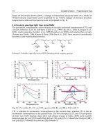
In 1976, Drozdov et al. (1976) proved lines in the photoluminescence spectra of deformed n-
and p-type Si associated with dislocations. The lines are denoted as D1 – D4 (figure 4). The
maximum position of the lines were measured at T = 4.2K as D1 = 0.812 eV, D2 = 0.875 eV,
D3 = 0.934 eV, and D4 = 1.000 eV. The relative intensity of D1 to D4 depend on the
dislocation density and distribution and can vary in different samples. The polarization of
the D-lines emission and their response to uniaxial stress has been utilized to establish their
relations to dislocations. Lines D1 and D2, on the one hand, and lines D3 and D4, on the
other, show similar shifts by applying uniaxial stress and therefore have been grouped as
pairs (Drozdov et al. 1977; Sauer et al., 1985). Polarization measurements were carried out to
determine the electric field vector of the luminescent light. Using three different
registration directions (211
,111,
[
011
]
), the vector within the primary slip plane, along
111, with a polarization of about 30% was found for D1/D2 (Weber, 1994). D3 and D4
exhibit an vector within the primary glide plane roughly along [011], i.e. along to the main
Burgers vector, and with a polarization of about 20%. These findings strongly point to the
dislocations as radiative centres for D3/D4. For D1/D2 the situation is more complex. The
energy positions of D3 and D4 depend on the distance between partial dislocations
suggesting that both originate from recombination processes at straight segments of 60°
dislocations (Sauer et al., 1986, 1994). In addition, photoluminescence measurements on
Fig. 4. Photoluminescence spectrum of dislocated silicon recorded at 80K. The spectrum
shows the presence of dislocation-induced D-bands (D1 – D4) besides the band-band
luminescence (BB).
Crystalline Silicon – Properties and Uses
66
dislocations in epitaxially grown SiGe layers refer to D3 as a phonon assisted replica of D4
(Weber & Alonso, 1990).
The origin of the D1 and D2 lines is still not understood. There are investigations referring
that both lines are related to impurity atoms in the dislocation core (Higgs et al., 1993),
dislocation jogs (Watson et al., 1998), or segments of dislocations (Lomer dislocations)
appearing due to dislocation reactions, multi-vacancy and/or self-interstitial clusters
trapped in the core (Jones et al., 2000).
4. Grain boundaries
Crystallization and recrystallization are typical processes to produce multi-crystalline silicon
as the mostly applied material in solar cell manufacture. Multi-crystalline silicon, or in
general polycrystalline materials, consists of numerous (single crystalline) grains with
different crystallographic orientations separated by grain boundaries. The geometry of a
grain boundary is macroscopically characterized by five degrees of freedom: three angles
define the crystallographic orientation of both crystals with respect to each other, while two
parameters describe the inclination of the grain boundary plane. To fully characterize the
boundary geometry on a microscopic level, three additional parameters are required to
define the atomic-scale relative translation of the two grains. Depending on the
misorientation, grain boundaries are of the tilt type, when the rotation axis lies in the
boundary plane, or of the twist type, when the rotation axis is normal to the boundary
plane. A general grain boundary may have tilt and twist components.
Based on previous consideration of Burgers, Bragg, and Frank (see Amelinckx, 1982), first
models of grain boundaries have been proposed by Shockley & Read (1949), Read &
Shockley (1950), van der Merwe (1949), and Cottrell (1953). Besides a classification into tilt
and twist boundaries, grain boundaries may be divided by their angle of misorientation
GB
into low-angle (
GB
< 5°) and large-angle grain boundaries. More comprehensive definitions
distinguish between singular, vicinal or general interfaces (Baluffi & Sutton, 1996), or
between general (or random) and special grain boundaries (Chadwick & Smith, 1976).
Special grain boundaries exhibit a periodic structure, while general grain boundaries show
no appearent periodicity.
Numerous investigations have been carried out about the structure of grain boundaries in
silicon. From these investigations it is concluded that (Seager, 1985):
1. Silicon grain boundaries are primarily composed of regular defects: perfect dislocations,
partial dislocations, and stacking faults. There are no evidences for distinct amorphous
phases at the grain boundary. This is true for all silicon materials grown by different
techniques.
2. Low-angle (
GB
< 5°) tilt and twist boundaries are not composed of regular arrays of
perfect dislocations. Instead, several types of dislocations are present in the same
boundary; some may be dissociated into partial dislocations forming a stacking fault in
between. Most of these low-angle grain boundaries are reconstructed such that no
dangling bonds remain.
3. Large-angle grain boundaries are usually composed of distinct facets. These facets with
lengths of one or more nanometers are subsections of the boundaries where bonding
rearrangements have occurred that are of a few known low-energy configurations.
These configurations can usually be predicted using the concepts of the coincidence site
lattice (CSL) theory (Gleiter & Chalmers, 1972; Chadwick & Smith, 1976; Sutton &
Structure and Properties of Dislocations in Silicon
67
Baluffi, 1995). The arrangement of these facets is not always a simple, repetitive one and
the average boundary interface angle can actually vary substantially over macroscopic
distances.
4. Even simple first-order twin boundaries can display this irregular faceted structure at
their interfaces. Dislocations frequently terminate at coherent twin boundaries, and the
resulting intersection points disturb the atomic arrangements on the boundary plane.
The interaction of intragranular dislocations with grain boundaries is an important issue
because grain boundaries are effective obstacles to dislocation motion. Dislocations coming
upon a boundary generally do not have the same Burgers vector and slip plane to glide into
the next grain. Most commonly, the elastic interaction between dislocations and grain
boundaries is repulsive and consequently the dislocations pile up at the boundary.
Dislocations, however, may also transmitted directly across the grain boundary if the slip
planes on both sides intersect along a line that lies in the boundary plane. For pure screw
dislocations, the Burgers vector remains unchanged. In contrast, the transmission of
dislocations with an edge component requires the formation of a residual grain boundary
dislocation with a Burgers vector equal to the difference of the Burgers vectors of the
incoming and outgoing lattice dislocations. A dislocation may alternatively be absorbed by
the boundary without emission of a dislocation in the adjacent grain. In this case, the lattice
dislocation fully dissociates.
Another important issue related to grain boundaries is the diffusion of impurities. It is
generally known that diffusion at grain boundaries is orders of magnitude faster compared
to volume diffusion, and it plays a major role in processes that involve material transport,
such as recrystallization, grain growth, grain boundary segregation, etc. Based on previous
analyses, Queisser et al. (1961) measured the phosphorous diffusion on a particular grain
boundary suggesting an enrichment of phosphorous near the boundary dislocations. More
recent investigations support the enhanced diffusion at grain boundaries but measurements
of the activation energy are quite different (Schimpf et al. 1994). Values of the activation
energy ranging from 1.4 eV to 2.9 eV were reported indicating the effect of the grain
boundary structure as well as the interaction with other impurities segregated at the
boundary on the diffusion. There is a number of other investigations dealing with the
diffusion of different elements into polycrystalline silicon. All these investigations show a
different behavior for various elements. For instance, an enhanced diffusion was proved for
boron and titanium (Corcoran & King, 1990), while the diffusion of Al is suppressed. Other
elements tend to diffuse out (Salman et al., 2007).
In order to overcome the difficulties arising from the analyses of polycrystalline materials
specific grain boundaries were of growing interest to study their structure and properties
(for instance, Bourret & Bacmann, 1987; Thibault-Desseaux et al., 1989). The realization of
the so-called bicrystals requires, however, a Czochralski growth process allowing only the
formation of specific grain boundaries such as = 9(122), = 13(510), and = 25(710)
(Aubert & Bacmann, 1987).
A first model of the electrical activity of grain boundaries in Ge was proposed by Taylor et
al. (1952). Based on measurements they concluded that the grain boundary acts as a
potential barrier due to surface states. The center zone with a high density of states
(assumed as broken bonds) and a space charge on either side represents a double Schottky
barrier. The current across the grain boundary, I, is then given by
=
[
(
−
)
∙
(
∓
/
)
]
/
[
1−
(
∓
/
)
]
, (13)
Crystalline Silicon – Properties and Uses
68
where µ is the carrier mobility, E is the electric field at the top of the barrier, n
B
the carrier
density at the barrier top, n
A
the carrier density on the bottom of the barrier, and V
AB
the
voltage measured across the barrier. The negative and positive signs are taken for electron
current and hole current, respectively. Using the Richardson equation for thermoionic
emission, Mueller (1961) write the zero-bias conductance G
0
of a grain boundary as
=(1−
)∙
(
/4
)
∙
/
∙∙
/
, (14)
with the capture rate, e the electron charge,
the average thermal velocity, N
c
the effective
number of states, and
0
the barrier height at equilibrium. The model of Taylor et al. (1952)
was developed further by Mataré (1984) and was successfully applied to interpret the
electronic properties of grain boundaries in bicrystals (Broniatowski, 1985; Bourgoin et al.
1987). Seager (1985) proposed another model by integrating tunneling and thermoionic
emission currents resulting in
=
∗
∙
[
(
)]
∙
(
)
[(
)/
)]
+
(
)
(15)
with A* as an effective Richardson constant, = E
C
-E
F
,
=
(
ℏ
/4
)
, N
d
the
dopant concentration, and m
t
as the tunneling mass. The second term in brackets of Eq. (15)
is the standard thermoionic emission, while the first term describes the thermoionic field
emission contributions to G
0
.
If a dc bias is applied to the grain boundary, the band diagram is modified. Using
simplifying assumptions (pinning of the Fermi level at the grain boundary, Mueller, 1961),
the energy density of grain boundary states with respect to the applied voltage is given by
Seager and Pike (1979) as
(
)
=
/
∙
/
+1+
´
(
+
)
/
(16)
for eV > kT. In Eq. (16)
B
´ =
/ and
B
is the barrier height given by
=
−
(
/
)
(17)
Models describing especially the minority carrier transport and recombination processes on
grain boundaries under optical illumination were presented, for instance, by Fossum &
Sundaresan (1982) and Joshi (1987). Assuming a Gaussian distribution of interface states
(other distributions were also discussed, see Joshi, 1987), the electron n(0) and hole
concentrations p(0) at the grain boundary are obtained as
(
0
)
=
∙exp
(
/
)
(18)
and
(
0
)
=
exp
(19)
Structure and Properties of Dislocations in Silicon
69
where n
i
is the intrinsic carrier concentration and
E
F
the separation of the quasi-Fermi
levels at the grain boundary.
E
F
is a function of the illumination level. Using the Shockley-
Read-Hall theory, Joshi (1987) calculated the steady-state recombination current density at a
grain boundary assuming a single interface energy level in the energy gap exists:
(
0
)
=
[
(
Δ
/
)
−1
]
∙
()
(
)
(
)
()
()
, (20)
where
c
and
n
are the Coulomb and neutral capture cross-sections for a recombination
center, respectively, n
gs
the energy distribution of the states and
= exp[(E-E
i
)/kT], where E
i
means the energy position of the mean value of the interface states distribution.
The increasing importance of multi-crystalline silicon in the production of solar cells results
in a huge number of publications related to the analyses of grain boundaries. The analyses
of trap levels on model grain boundaries were extensively investigated by Broniatowski
(1985). Numerous measurements on individual grain boundaries in multi-crystalline silicon
were presented. Recent results about the electrical activity of grain boundaries obtained by
EBIC methods were published, for instance, by Chen et al. (2010), Sekiguchi et al. (2011), or
Pandelov et al. (2002). These papers refer to numerous others published previously. Caused
by the high local resolution EBIC methods were also utilized to study the segregation of
dopands or metallic impurities on grain boundaries (e.g. Seibt et al., 2009). The passivation
of interface states on grain boundaries by hydrogen was studied as well (Rinio et al. 2006;
Chen et al., 2005).
Furthermore, luminescence-based techniques are widely applied in the characterization of
grain boundaries in solar cell materials. Cathodoluminescence (Vernon-Parry et al., 2005)
and photoluminescence (Mchedlidze et al., 2010; Dreckschmidt & Möller, 2011) are useful
tools to characterize defects at grain boundaries and different multi-crystalline bulk and thin
film materials. The high sensitivity of the band-to-band emission of silicon to recombination
activity (Würfel, 1982) results in the development of micro-photoluminescence spectroscopy
used to study individual defects as well as to characterize the quality of whole solar cell
wafers. The method allows the characterization of impurities (metal precipitates) and their
effect on the recombination behavior of extended defects (Gundel et al. 2009, 2010).
Recently, the D-lines appearing in the photoluminescence spectrum of dislocated silicon
were used as well. First results using photoluminescence (Schmid, 2011) and
cathodoluminescence were reported (Lee et al., 2009; Sekiguchi et al. 2010). Another
approach to study electrically active defects in multicrystalline materials is the so-called
dark lock-in thermography (DLIT, Breitenstein et al., 2010).
5. Characterization of individual dislocations
A fundamental problem in studying dislocations is the realization of defined arrangements
of these defects. Some of the methods need a higher concentration of the defects to attain the
detection limit (such as EPR). In contrast, other methods, as electron microscopy, require
only a few or individual dislocations to obtain reasonable results. The dominant method to
produce defined dislocation arrangements is plastic deformation. Plastic deformation,
however, result also in a large number of point defects and defect reactions making it
sometimes difficult to interpret experimental data (Alexander et al., 1983; Alexander &
Teichler, 1991). In order to avoid interactions between dislocations or between dislocations
and other defects, methods are required allowing the realization and analyses of only a few
Crystalline Silicon – Properties and Uses
70
dislocations or, in the ideal case, of an individual dislocation. First attempts can be traced
back into the 1970th. Eremenko et al. (see Shikin & Shikina, 1995) measured the current-
voltage characteristics of a 60° dislocation. Similar experiments were also done by Milshtein
(1979) a few years later. Their measurements demonstrated a diode behavior of the
dislocation. The dislocation was assumed to pass the whole specimen and metallic tips were
used as contacts which, however, were singnificantly larger than the dislocation diameter.
Another approach to realize defined dislocation arrangements was the application of silicon
and germanium bicrystals (Thibault-Desseaux et al., 1989). As pointed out before, only
specific orientations of grain boundaries are viable by the Czochralski growth process.
Another method to realize defined dislocation arrangements in a reproducible way is
semiconductor wafer direct bonding. For wafer bonding commercially available wafers are
used making it possible to realize any grain boundary. Especially small-angle grain
boundaries having rotation angles below 1° are of interest allowing to separate dislocations
by a few hundred nanometers. Such distances are large enough to analyze only a small
number or individual dislocations.
The principle of semiconductor wafer direct bonding originally developed to produce
silicon on insulator (SOI) substrates and three-dimensional micro-electromechanical systems
(MEMS) was comprehensively described elsewhere (Tong & Gösele, 1998). If the native
oxide is removed from the wafers, two Si surfaces are brought into contact (hydrophobic
wafer bonding). A subsequent annealing transforms the original adhesion forces into Si-Si
bonds via the interface. Crystal defects (dislocations) are generated forming a two-
dimensional network (or grain boundary) in order to match both crystal lattices. The
structure of the dislocation network depends on the surface orientation of both wafers.
Screw dislocation networks, networks dominated by 60°, and interactions between both
types of networks were realized and studied in detail (for instance, Reiche (2008)). The mesh
size of the network or, the dislocation distance, is reproducibly adjusted by controlling the
tilt and twist misorientation angles which can be calculated using Frank´s formula
(Amelinckx, 1982). Dislocation distances of more than 100 nm are obtained by using
misorientation angles below 0.1°. Note that misorientation angles down to 0.005° were
realized using aligned wafer bonding processes (Wilhelm et al., 2008).
Properties of dislocation networks formed by semiconductor wafer direct bonding were
described in numerous publications (for reviews see, e.g. Kittler et al., 2007; Kittler & Reiche,
2009). The dislocation networks may be considered as model structures resulting in a lot of
new information about the structure and properties of dislocations. The electrical properties
of bonded hydrophobic silicon wafers were studied for the first time by Bengtsson et al.
(1992) using capacitance-voltage measurements. More recent EBIC analyses proved barrier
heights generally smaller than 100 meV for different types of bonded hydrophobic wafers
(Kittler & Reiche, 2009). The concentration of deep levels along the interface was determined
to be a few 10
5
per cm.
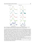
The luminescence properties of dislocation networks were also studied. Figure 5a shows the
luminescence spectra of different bonded samples. The spectra are obtained from samples
having different misorientation. Detailed photoluminescence and cathodoluminescence
measurements provide direct evidence that the wavelength of light emitted from the
dislocation network could be tailored to some extent by misorientation of the wafers during
the bonding procedure. D1 or D3 lines have the largest intensity in the spectra due to the
variation of the twist angle from 8.2° to 9°. Thus the luminescence spectrum can be tailored
Structure and Properties of Dislocations in Silicon
71
by the misorientation angles in a controlled manner and the dominance of either D1 or D3
radiation can be attained. Further investigations refer that screw dislocations dominantly
effect the intensity of the D1 line. The photoluminescence spectra of three different
dislocation networks are presented in figure 5b. The corresponding electron microscope
images are shown in figure 5c. The dislocation network DN#1 is dominated by 60°
dislocations running in the image parallel with a distance in between of about 30 nm. The
network of the 60° dislocations is superposed by an additional network of screw
dislocations having distances of more than 2 µm (not shown in the image). The other
networks in figure 5c (DN#2, DN#3) are characterized by more or less hexagonal meshes
caused by the interaction of two networks of 60° dislocations and screw dislocations, both
with nearly the same dislocation distances therein. The photoluminescence spectra recorded
at low temperature (80K) and room temperature show the presence of the D1-line around
0.7 0.8 0.9 1.0 1.1 1.2 1.3
Intensity (a.u.)
Energy (eV)
a
b
c
D1 D2 D3 D4
Twist Tilt
a) 8.2° 0.2°
b) 9.0° 0.2°
c) 1.5° 0.53°
(a) (b)
(c)
Fig. 5. The impact of the misorientation and dislocation structure on the luminescence
spectra of dislocation networks. (a) The effect of misorientation (tilt and twist components).
Cathodoluminescence spectra recorded at 80K. Photoluminescence spectra measured at 80K
and room temperature (b) of three dislocation networks shown in (c).
Crystalline Silicon – Properties and Uses
72
(figure 5b). The spectra clearly prove the different intensity behavior depending on the
dislocation structure and distance of the screw dislocations. The intensity of the D1-line is
lowest in the spectrum of sample DN#1, characterized by the largest distance of screw
dislocations, and increases as the distance of the screw dislocations decreases. The distance
of screw dislocations in these particular samples is 15 nm (DN#2) and 32 nm (DN#3). Note
that significant intensities of the D1-line are measured for DN#2 and DN#3 which are
considerably stronger than that of the band-to-band-luminescence even at room
temperature. According to these results it is suggested that radiative recombination is
mainly caused by screw dislocations while 60° dislocations attribute preferentially to the
non-radiative recombination.
A combination of wafer bonding with preparation methods to separate individual
dislocations or a small number of dislocations allows the measurement of their electronic
properties by elimination of interactions in between. As shown before, twist angles between
two bonded Si wafers below 0.1° result in dislocation distances of more than 100 nm. Using
photolithography and etching techniques, individual dislocations can be separated and
measured. Typical structures applied were diodes and metal-oxide-semiconductor field-
effect transistors (MOSFETs) (Reiche et al. 2010, 2011). The presented data clearly showed an
indirect behavior of the drain current on the number of dislocations in the channel. The fact
that the highest current is obtained if only a few dislocations are present allows the
conclusion that electrically active centers in the dislocation core of the straight dislocation
segments are responsible for the electron transport while dislocation nodes and dislocation
segments oriented orthogonal to the channel direction act as “scattering centers” and reduce
the carrier transport.
The single-electron tunneling on dislocations was recently studied by Ishikawa et al. (2006)
on nMOSFETs prepared on dislocation networks produced by wafer bonding of SOI wafers.
Measurements were done using a back gate contact (oxide thickness 400nm). Low-
temperature measurements (T=15K) proved oscillations in the drain current – gate voltage
curves indicating single-electron tunneling (Coulomb blockade oscillations). The lateral size
of the Coulomb islands was estimated to be about 20 nm which agreed with the dislocation
distance. From this Ishikawa et al. (2006) concluded that Coulomb islands are related to the
dislocation nodes in the screw dislocation network. Very recent measurements at T = 4K by
the authors proved also the existence of Coulomb blockade oscillations. Using nMOSFETs
and applying a front side gate contact (gate oxide thickness 6 nm) lateral sizes of the
Coulomb island of about 6 nm were extracted which do not correspond to dislocation nodes.
Furthermore, a different behavior is observed for screw and mixed dislocations resulting
from the reaction of screw and 60° dislocations. The single-electron tunneling was proved
for one set (screw dislocations), while the other shows a more two-dimensional charac-
teristics indicated by a staircase structure.
6. Acknowledgment
We would like to thank T. Arguirov, A. Hähnel, T. Mchedlidze, R. Scholz, W. Seifert, and O.
Vyvenko for supporting this work. Parts of this work were financially supported by the
German Federal Ministry of Education and Research in the framework of the SiliconLight
project (contract no. 13N9734) and the SiGe-TE project (contract no. 03X3541B).
Structure and Properties of Dislocations in Silicon
73
7. References
Alexander, H. (1986). Dislocations in Covalent Crystals, in: Dislocation in Solids, Vol. 7,
F.R.N. Nabarro, pp. 113-234, North-Holland, Amsterdam
Alexander, H. (1991). Dislocations in Semiconductors, in: Polycrystalline Semiconductors II,
J.H. Werner and H.P. Strunk, Springer Proc. In Physics, Vol. 54, Springer, Berlin,
pp. 2-12
Alexander, H. & Teichler, H. (1991). Dislocations, in: Materials Science and Technology, Vol. 4.
Electronic Structure and Properties of Semiconductor, W. Schröter, VCH, Weinheim,
pp. 249-319
Alexander, H. & Teichler, H. (2000). Dislocations, in: Handbook of Semiconductor Technology,
K.A: Jackson and W. Schröter, Wiley-VCH, Weinheim, pp. 291-376
Alexander, H., Kisielowski-Kemmerich, C., and Weber, E.R. (1983). Investigations of Well
Defined Dislocations in Silicon, Physica B, Vol. 116, pp. 583-593
Amelinckx, S. (1982). Dislocations in Particular Structures, in: Dislocation in Solids, Vol. 2,
F.R.N. Nabarro, pp. 67-460, North-Holland, Amsterdam
Aubert, J.J. & Bacmann, J.J. (1987). Czochralski Growth of Silicon Bicrystals, Revue Phys.
Appl., Vol. 22, No. 7, pp. 515-518
Baluffi, R.W. & Sutton, A.P. (1996). Why Should We Interested in the Atomic Structure of
Interfaces?, Mat. Sci. Forum, Vol. 207-209, pp. 1-12
Bangert, U., Harvey, A.J., Jones, E., Fall, C.J., Blumenau, A.T., Briddon, R., Schreck, M., and
Hörmann, F. (2004). Dislocation-Induced Electronic States and Point Defect
Atmospheres Evidenced by Electron Energy Loss Imaging, New J. Phys., Vol. 6, pp.
184-189
Bardeen, J. & Shockley, W. (1950). Deformation Potentials and Mobilities in Non-Polar
Crystals, Phys. Rev., Vol. 80, No. 1, pp. 72-80
Benetto, J., Nunes, R.W., and Vanderbilt, D. (1997). Period-Double Structure for the 90°
Partial Dislocation in Silicon, Phys. Rev. Lett., Vol. 79, No. 2, pp. 245-248
Bengtsson, S., Andersson, G.I., Andersson, M.O., and Engström, O. (1992). The Bonded
Unipolar Silicon-Silicon Junction, J. Appl. Phys., Vol. 72, No. 1, pp. 124-140
Bigger, J.R.K., McInnes, D.A., Sutton, A.P., Payne, M.C., Stich, I., King-Smith, R.D., Bird,
D.M., and Clarke, L.J. (1992). Atomic and Electronic Structures of the 90° Partial
Dislocation in Silicon, Phys. Rev. Lett., Vol. 69, No. 15, pp. 2224-2227
Bourgoin, J.C., Mauger, A., and Lannoo, M. (1987). Electronic Properties of Grain
Boundaries in Semiconductors, Revue Phys. Appl., Vol. 22, No. 7, pp. 579-583
Bourret, A. & Bacmann, J.J. (1987). Atomic Structure of Grain Boundaries in Semiconductors,
Revue Phys. Appl., Vol. 22, No. 7, pp. 563-568
Breitenstein, O. & Wosinski, T. (1983). Scanning-DLTS Investigation of the EL 2 Level in
Plastically Deformed GaAs, Phys. Stat. Sol. (a), Vol. 77, K107-K110
Breitenstein, O., Bauer, J., Altermatt, P.P., and Ramspeck, K. (2010). Influence of Defects on
Solar Cell Characteristics, Solid State Phenom., Vol. 156-158, pp. 1-10
Broniatowski, A. (1985). Electronic States at Grain Bounaries in Semiconductors, in:
Polycrystalline Semiconductors, Physical Properties and Applications, G. Harbecke, pp.
95-117, Springer, Berlin
Bulatov, V.V., Yip, S., and Argon, A.S. (1995). Atomic Modes of Dislocation Mobility in
Silicon, Phil. Mag. A, Vol. 72, No. 2, pp. 453-496
Crystalline Silicon – Properties and Uses
74
Bulatov, V.V., Justo, J.F., Cai, W., Yip, S., Argon, A.S., Lenosky, T., de Koning, M., and Diaz
de la Rubia, T. (2001). Parameter-Free Modelling of Dislocation Motion: The Case of
Silicon, Phil. Mag., Vol. 81, No. 5, pp. 1257-1281
Bulatov, V.V. & Cai, W. (2006). Computer Simulations of Dislocations, Oxford Univ. Press,
Oxford
Burgers, W.G. & Burgers, J.M. (1935). First report on viscosity and plasticity. Kon. Nederl.
Akad. v. Wet., Sect. 1, Vol. 15, No. 3
Burgers, J.M. (1939). Some Considerations on the Fields of Stress Connected with
Dislocations in a Regular Crystal Lattice. Kon. Nederl. Akad. v. Wet. Vol. 42, pp. 293-
325
Burgers, J.M. (1940). Geometrical Considerations Concerning the Structural Irregularities to
be Assumed in a Crystal, Proc. Phys. Soc. London, Vol. 52, pp. 23-33
Chadwick, G.A. & Smith, D.A. (1976). Grain Boundary Structure and Properties, Academic
Press, London
Chelikowsky, J.R. (1982). 30° Partial Dislocations in Silicon: Absence of Electrically Active
States, Phys. Rev. Lett., Vol. 49, No. 21, pp. 1569-1572
Chen, J., Yang, D., Xi, Z., and Sekiguchi, T. (2005). Electron-Beam-Induced Current Study of
Hydrogen Passivation on Grain Boundaries in Multicrystalline Silicon: Influence of
GB Character and Impurity Contamination, Physica B, Vol. 364, No. 1, pp. 162-169
Chen, J., Chen, B., Lee, W., Fukuzawa, M., Yamada, M., and Sekiguchi, T. (2010). Grain
Boundaries in Multicrystalline Si, Solid State Phenom., Vol. 156-158, pp. 19-26
Cockayne, D.J.H., Ray, I.L.F. and Whelan, M.J. (1969). Investigations of Dislocation Strain
Fields Using Weak Beams, Phil. Mag. Vol. 20, pp. 1265-1270
Corcoran, Y.L. & King, A.H. (1990). Grain Boundary Diffusion and Growth of Titanium
Silicide Layers on Silicon, J. Electron. Mat., Vol. 19, No. 11, pp. 11771183
Cottrell, A.H. (1953). Dislocations and Plastic Flow in Crystals, Clarendon, Oxford
Csányi, G., Engeness, T.D., Ismail-Beigi, S., and Arias, T.A. (2000). New Physics of the 30°
Partial Dislocation in Silicon Revealed Through ab initio Calculations, J. Phys.:
Condens. Mater. Vol. 12, pp. 10029-10037
Dehlinger, U. & Kochendörfer, A. (1940). Eigenbewegungen in Kristallgittern. Z. Phys. Vol.
116, pp. 576-585
Donolato, C. (1979). Contrast and Resolution of SEM Charge-Collection Images of
Dislocations, Appl. Phys. Lett., Vol. 34, No. 1, pp. 80-81
Donolato, C. (1983). Quantitative Evaluation of the EBIC Contrast of Dislocations, J. Physique
Coll., Vol. 44, No. 9, pp. C4-269 – 275
Dreckschmidt, F. & Möller, H J. (2011). Defect Luminescence at Grain Boundaries in
Multicrystalline Silicon, Phys. Stat. Sol. (c) Vol. 8, No. 4, pp. 1356-1360
Drozdov, N.A., Patrin, A.A., and Tkachev, V.D. (1976). Recombination Radiation on
Dislocations in Silicon, Pisma Zh. Eksp. Teor. Fiz., Vol. 23, No. 11, pp. 651-653, Sov.
Phys. JETP Lett. Vol. 23, pp. 597-599
Drozdov, N.A., Patrin, A.A., and Tkachev, V.D., On the Nature of the Dislocation
Luminescence in Silicon, Phys. Stat. Sol. (b), Vol. 83, No. 2, pp. K137-K139
Duesbery, M.S. & Richardson, G.Y. (1991). The Dislocation Core in Crystalline Materials,
Rev. Solid State Mater. Sci. Vol 17, No. 1, pp. 1-46
Structure and Properties of Dislocations in Silicon
75
Duesbery, M.S., Joos, B., and Michel, D.J. (1991). Dislocation Core Studies in Empirical
Silicon Models, Phys. Rev. B, Vol. 43, No. 6, pp. 5143-5146
Duesbery, M.S. & Joós, B. (1996). Dislocation Motion in Silicon: The Shuffle-Glide
Controversy, Phil Mag. Lett., Vol. 74, No. 4, pp. 253-258
Eshelby, J.D. (1949). Edge Dislocations in Anisotropic Materials. Phil. Mag. Vol. 7, No. 40, pp.
903-912
Figielski, T. (1990). Electron Emission from Extended Defects: DLTS Signal in Case of
Dislocation Traps, Phys. Stat. Sol. (a), Vol. 121, No. 1, pp. 187-193
Fossum, J.G. & Sundaresan, R. (1982). Analysis of Minority-Carrier Transport in Polysilicon
Devices, IEEE Trans. Electron. Dev., Vol. ED-29, No. 8, pp. 1185-1197
Frank, F.C. (1951). Crystal Dislocations – Elementary Concepts and Definitions, Phil. Mag.
Vol. 42, No. 331, pp. 809-819
Friedel, J. (1979). Dislocations – an Introduction, in: Dislocation in Solids, Vol. 1, F.R.N.
Nabarro, pp. 1-32, North-Holland, Amsterdam
Gallagher, C.J. (1952). Plastic Deformation of Germanium and Silicon, Phys. Rev. Vol. 88, No.
4, pp. 721-722
George, A. & Yip, S. (2001).Preface to the Viewpoint Set on: Dislocation Mobility in Silicon,
Scripta Mat., Vol. 45, pp. 1233-1238
Gleiter, H. & Chalmers, B. (1972). High-Angle Grain Boundaries, Pergamon Press, Oxford
Gomez, A., Cockayne, D.J.H., Hirsch, P.B., and Vitek, V. (1974). Dissociation of Near-Screw
Dislocations in Germanium and Silicon, Phil. Mag. Vol. 31, pp. 105-113
Gomze, A.M. & Hirsch, P.B. (1977). On the Mobility of Dislocations in Germanium and
Silicon, Phil. Mag. Vol. 36, No.1, pp. 169-179
Gundel, P. Schubert, M.C., Kwapil, W., Schön, J., Reiche, M., Savin, H., Yli-Koski, M., Sans,
J.A., Martinez-Criado, G., Seifert, W., Warta, W., and Weber, E.R. (2009). Micro-
Photoluminescence Spectroscopy on Metal Precipitates in Silicon, Phys. Stat. Sol.
RRL, pp. 1-3
Gundel, P., Schubert, M.C., Heinz, F.D., Kwapil, W., Warta, W., Martinez-Criado, G., Reiche,
M., and Weber, E.R. (2010). Impact of Stress on the Recombination at Metal
Precipitates in Silicon, J. Appl. Phys. 108, pp. 103707-1 - 5
Heggie, M. & Jones, R. (1982). Glide of Partial Dislocations in Silicon, J. Physique, Coll., Vol.
43, No. 10, pp. 45-50
Heggie, M. & Jones R. (1983). Solitons and the Electrical and Mobility Properties of
Dislocations in Silicon, Phil. Mag., Vol. 48, No. 4, pp. 365-377
Heggie, M.I., Jones, R., and Umerski, A. (1993). Ab Initio Energy Calculations of Impurity
Pinning in Silicon, Phys. Stat. Sol. (a), Vol. 138, pp. 383-387
Higgs, V., Lightowlers, E.C., Fitzgerald, E.A., Xie, Y.H., and Silverman, P.J. (1993).
Characterization of Compositionally Graded Si
1-x
Ge
x
Alloy Layers by
Photoluminescence Spectroscopy and by Cathodoluminescence Spectroscopy and
Imaging, J. Appl. Phys., Vol. 73, No. 4, pp. 1952-1956
Hirsch, P.B. (1979). Recent Results on the Structure of Dislocations in Tetrahedrally
Coordinated Semiconductors, J. Physique, Coll., Vol. 40, No. 6, pp. C6-27 - 32
Hirsch, P.B. (1985). Dislocations in Semiconductors, Mat. Sci. Technol., Vol. 1, No. 9, pp. 666-
677
Hirth, J.P. & Lothe, J. (1982). Theory of Dislocations, Wiley Interscience, New York
Crystalline Silicon – Properties and Uses
76
Hornstra, J. (1958). Dislocations in the Diamond Lattice, J. Phys. Chem. Solids, Vol. 5, pp. 129-
141
Ishikawa, Y., Yamamoto, C., and Tabe, M. (2006). Single-Electron Tunneling in a Silicon-On-
Insulator Layer Embedding an Artificial Dislocation Network, Appl. Phys. Lett., Vol.
88, pp. 073112-1 - 3
Jones, R., Umerski, A., Stich, P., Heggie, M.I., and Öberg, S. (1993). Density Functional
Calculations of the Structure and Properties of Impurities and Dislocations in
Semiconductors, Phys. Stat. Sol. (a), Vol. 138, pp. 369-381
Jones, R., Coomer, B.J., Goss, J.P., Öberg, S., and Briddon, P.R. (2000). Intrinsic Defects and
the D1 to D4 Optical Bands Detected in Plastically Deformed Si, Phys. Stat. Sol. (b),
Vol. 222, No. 1, pp. 133-140
Joshi, D.P. (1987). Grain Boundary Recombination in Polycrystalline Silicon Under Optical
Illumination, Phys. Stat. Sol. (a), Vol. 108, No. 2, pp. 213-218
Kisielowski-Kemmerich, C. (1990). Vacancies and Their Complexes in the Core of Screw
Dislocations: Models which Account for ESR Investigations of Deformed Silicon,
Phys. Stat. Sol. (b), Vol. 161, pp. 11-42
Keyes, R.W. (1960). The Effects of Elastic Deformation on the Electrical Conductivity of
Semiconductors, Solid State Phys., Vol. 11, pp. 149-221
Kittler, M., Yu, X., Mchedlidze, T., Arguirov, T., Vyvenko, O.F., Seifert, W., Reiche, M.,
Wilhelm, T., Seibt, M., Voß, O., Wolff, A., and Fritzsche, W. (2007). Regular
Dislocation Networks in Silicon as a Tool for Nanostructure Devices Used in
Optics, Biology, and Electronics, Small, Vol. 3, No. 6, pp. 964-973
Kittler, M. & Reiche, M. (2009). Dislocations as Active Components in Novel Silicon Devices,
Adv. Eng. Mater. Vol. 11, No. 4, 249-258
Kochendörfer, A. (1938). Theorie der Kristallplastizität, Z. Phys. Vol. 108, No. 3-4, pp. 244-
264
Kveder, V., Kittler, M., and Schröter, W. (2001). Recombination Activity of Contaminated
Dislocations in Silicon: A Model Describing Electron-Beam-Induced Current
Contrast Behavior, Phys. Rev. B, Vol. 63, pp. 115208-1 - 11
Kveder, V. & Kittler, M. (2008). Dislocations in Silicon and D-Band Luminescence for
Infrared Light Emitters, Mat. Sci. Forum, Vol. 590, pp. 29-56
Labusch, R. & Schröter, W. (1980). Electrical Properties of Dislocations in Semiconductors,
in: Dislocation in Solids, Vol. 5, F.R.N. Nabarro, pp. 127-191, North-Holland,
Amsterdam
Lang, D.V. (1974). Deep-Level Transient Spectroscopy: A New Method to Characterize
Traps in Semiconductors, J. Appl. Phys., Vol. 45, No. 7, pp. 3023-3032
Lee, W., Chen, J., Chen, B., Chang, J., and Sekiguchi, T. (2009). Cathodoluminescence Study
of Dislocation-Related Luminescence From Small-Angle Grain Boundaries in
Multicrystalline Silicon, Appl. Phys. Lett., Vol. 94, pp. 112103-1 - 3
Lehto, N. & Öberg, S. (1998) Effects of Dislocation Interactions: Application to the Period-
Double Core of the 90° Partial in Silicon, Phys. Rev. Lett., Vol. 80, No. 25, pp. 5568-
5571
Li, C., Meng, Q., Zhong, K., and Wang, C. (2008). Computer Simulation of the 60°
Dislocation Interaction with Vacancy Cluster in Silicon, Phys. Rev. B, Vol. 77, pp.
045211-1 – 045211-5
Structure and Properties of Dislocations in Silicon
77
Lodge, K.W., Lapiccirella, A., Battistoni, C., Tomassini, N., and Altmann, S.L. (1989). The 90°
Partial Dislocation in Silicon: Geometry and Electronic Structure, Phil. Mag. A, Vol.
60, No. 5, pp. 643-651
Love, A.E.H. (1927). A Treatise on the Mathematical Theory of Elasticity, Cambridge University
Press, Cambridge, p. 221
Marklund, S. (1979). Electron States Associated with Partial Dislocations in Silicon, Phys.
Stat. Sol. (b), Vol. 92, pp. 83-89
Marklund, S. (1981). Energy Levels of Intrinsic and Extrinsic Stacking Faults in Silicon, Phys.
Stat. Sol. (b), Vol. 108, pp. 97-102
Marklund, S. (1983). Structure and Energy Levels of Dislocations in Silicon, J. Physique, Coll.,
Vol 44, No. 9, C4-25 - 35
Mataré, H.F. (1984). Carrier Transport at Grain Boundaries in Semiconductors, J. Appl. Phys.,
Vol. 56, No. 10, pp. 2605-2631
Mattheiss, L.F. & Patel, J.R. (1981). Electronic Stacking Fault States in Silicon, Phys. Rev. B,
Vol. 23, No. 10, 5384-5396
Mchedlidze, T., Arguirov, T., Kouteva-Argoirova, S., and Kittler, M. (2010). Characterization
of Thin Film Photovoltaic Material Using Photoluminescence and Raman
Spectroscopy, Solid-State Phenom. Vol. 156-158, pp. 419-424
Milshtein, S. (1979). Application of Dislocation-Induced Potentials in Si and Ge, J. Physique,
Coll., Vol. 40, No. 6, pp. C6-207 - 211
Mueller, R.K. (1961). Current Flow Across Grain Boundaries in n-Type Germanium I, J. Appl.
Phys., Vol. 32, No. 4, pp. 635-639
Nabarro, F.R.N. (1947). Dislocations in a Simple Cubic Lattice. Proc. Phys. Soc. London, Vol.
59, pp. 256-272
Northrup, J.E., Cohen, M.L., Chelikowsky, J.R., Spence, J., and Olsen, A. (1981). Electronic
Structure of the Unreconstructed 30° Partial Dislocation in Silicon, Phys. Rev. B, Vol.
24, No. 8, pp. 4623-4628
Orowan, E. (1934). Zur Kristallplastizität III. Z. Phys. Vol. 89, pp. 634-659
Pandelov, S., Seifert, W., Kittler, M., and Reif, J. (2002). Analysis of Local Electrical
Properties of Grain Boundaries in Si by Electron-Beam-Induced-Current
Techniques, J. Phys.: Condens. Matter, Vol. 14, pp. 13161-13168
Pasemann, L. (1981). A Contribution to the Theory of the EBIC Contrast of Lattice Defects in
Semiconductors, Ultramicroscopy, Vol. 6, pp. 237-250
Pearson, G.L., Read, W.T., and Morin, F.J. (1954). Dislocations in Plastically Deformed
Germanium. Phys. Rev. Vol. 93, No. 4, pp. 666-667
Peierls, R. (1940). The Size of a Dislocation. Proc. Phys. Soc. London, Vol. 52, pp. 34-37
Polanyi, M. (1934). Über eine Art Gitterstörung, die einen Kristall plastisch machen könnte.
Z. Phys. Vol. 89, pp. 660-664
Queisser, H.J., Hubner, K., and Shockley, W. (1961). Diffusion Along Small-Angle Grain
Boundaries in Silicon, Phys. Rev. Vol. 123, No. 4, pp. 1245-1254
Ray, I.L.F. & Cockayne, D.J.H. (1971). The Dissociation of Dislocations in Silicon,
Proc. R. Soc.
London, A, Vol. 325, pp. 543-554
Read, W.T. (1954a). Theory of Dislocations in Germanium, Phil. Mag. Vol. 45, No. 367, pp.
775-796
Crystalline Silicon – Properties and Uses
78
Read, W.T. (1954b). Statistics of the Occupation of Dislocation Acceptor Centres, Phil. Mag.
Vol. 45, No. 370, pp. 1119-1128
Read, W.T. & Shockley, W. (1950). Dislocation Models of Crystal Grain Boundaries, Phys.
Rev., Vol. 78, No. 3, pp. 275-289
Reiche, M. (2008). Dislocation Networks Formed by Silicon Wafer Direct Bonding, Mater. Sci.
Forum, Vol. 590, pp. 57-78
Reiche, M., Kittler, M., Buca, D., Hähnel, A., Zhao, Q T., Mantl, S., and Gösele, U. (2010).
Dislocation-Based Si-Nanodevices, Jpn. J. Appl. Phys., Vol. 49, pp. 04DJ02-1 - 5
Reiche, M., Kittler, M., Scholz, R., Hähnel, A., and Arguirov, T. (2011). Structure and
Properties of Dislocations in Interfaces of Bonded Silicon Wafers, J. Phys. Conf. Ser.,
Vol. 281, pp. 012017-1 - 10
Rinio, M., Kaes, M., Hahn, G., and Borchert, D. (2006). Hydrogen Passivation of Extended
Defects in Multicrystalline Silicon Solar Cells, Proc. 21
st
Europ. Photovolt. Solar
Energy Conf., Dresden
Salman, F., Arnold, J., Zhang, P., Chai, G., Stevie, F.A., and Chow, L. (2007). Redistribution
of Implanted Species in Polycrystalline Silicon Films on Silicon Substrate, Defect &
Diff. Forum, Vol. 264, pp. 7-12
Sauer, R., Weber, J., Stolz, J., Weber, E.R., Küsters, K H., and Alexander, H. (1985).
Dislocation-Related Photoluminescence in Silicon, Appl. Phys. A, Vol. 36, No. 1, pp.
1-13
Schimpf, K., Palm, J., and Alexander, H. (1994). Enhanced Diffusion of Phosphorous at
Grain Boundaries in Multicrystalline Silicon, Cryst. Res. Technol. Vol. 29, No. 8, pp.
1123-1129
Schmid, R.P., Mankovics, D., Arguirov, T., Mchedlidze, T., and Kittler, M. (2011). Novel
Imaging Techniques for Dislocation-Related D1-Photoluminescence of
Multicrystalline Si Wafers – Two Different Approaches, Phys. Stat. Sol. (c), Vol. 8,
No. 4, pp. 1297-1301
Schröter, W. (1969). Trägerbeweglichkeit in verformtem Germanium, Phys. Stat. Sol., Vol. 31,
No. 1, pp. 177-186
Schröter, W. & Labusch, R. (1969). Electrical Properties of Dislocations in Ge and Si. Phys.
Stat. Sol. Vol. 36, pp. 539-550
Schröter, W. & Cerva, H. (2002). Interaction of Point Defects with Dislocations in Silicon and
Germanium: Electrical and Optical Effects, Solid State Phenom. Vol. 85-86, pp. 67-144
Seager, C.H. (1985). Grain Boundaries in Polycrystalline Silicon, Ann. Rev. Mater. Sci., Vol.
15, pp. 271-302
Seager, C.H. & Pike, G.E. (1979). Grain Boundary States and Varistor Behavior in Silicon
Bicrystals, Appl. Phys. Lett., Vol. 35, No. 9, pp. 709-711
Seibt, M., Khalil, R., Kveder, V., and Schröter, W. (2009a). Electronic States at Dislocations
and Metal Silicide Precipitates in Crystalline Silicon and Their Role in Solar Cell
Materials, Appl. Phys. A, Vol. 96, pp. 235-253
Seibt, M., Abdelbarey, D., Kveder, V., Rudolf, C., Saring, P., Stolze, L., and Voß, O. (2009b).
Structure, Chemistry and Electrical Properties of Extended Defects in Crystalline
Silicon for Photovoltaics, Phys. Stat. Sol. (c), Vol. 6, No. 8, pp. 1847-1855
Seitz, F. (1952). The Plasticity of Silicon and Germanium, Phys. Rev. Vol. 88, No. 4, pp. 722-
724
Structure and Properties of Dislocations in Silicon
79
Sekiguchi, T., Chen, J., Lee, W., and Onodera, H. (2011). Electrical and Optical Activities of
Small Angle Grain Boundaries in Multicrystalline Si, Phys. Stat. Sol. (c), Vol. 8, No.
4, pp. 1347-1350
Shikin, V.B. & Shikina, Y.V. (1995). Charged Dislocations in Semiconductor Crystals, Usp.
Fiz. Nauk, Vol. 165, No. 8, pp. 887-917, Physics-Uspekhi, Vol. 38, No. 8, pp. 845-875
Shockley, W. (1953). Dislocations and Edge States in the Diamond Crystal Structure, Phys.
Rev., Vol. 91, p. 228
Shockley, W. & Read, W.T. (1949). Quantitative Predictions from Dislocation Models of
Crystal Grain Boundaries, Phys. Rev., Vol. 75, p. 692
Spence, J.C.H. (2007). Experimental studies of Dislocation Core Defects, in: Dislocation in
Solids, Vol. 13, F.R.N. Nabarro and J.P. Hirth, pp. 419-452, Elsevier, Amsterdam
Sutton, A. & Baluffi, R.W. (1995). Interfaces in Crystalline Materials, Oxford University Press,
Oxford
Taylor, G.I. (1934a). The Mechanism of Plastic Deformation of Crystals. Part I Theoretical.
Proc. R. Soc. London, Vol. 145, No. 855, pp. 362-387
Taylor, G.I. (1934b). The Mechanism of Plastic Deformation of Crystals. Part II. -
Comparison with Observations. Proc. R. Soc. London, Vol. 145, No. 855, pp. 388-404
Taylor, W.E., Odell, N.H., and Fan, H.Y. (1952). Grain Boundary Barriers in Germanium,
Phys. Rev., Vol. 88, No. 4, pp. 867-875
Thibault-Desseaux, J., Putaux, J.L., Bourret, A., and Kirchner, H.O.K. (1989). Dislocations
Stopped by the = 9(122) Grain Boundary in Si. An HREM Study of Thermal
Activation, J. Physique, Vol. 50, pp. 2525-2540
Tong, Q.Y. & Gösele, U. (1998). Semiconductor Wafer Bonding. Science and Technology, Wiley,
New York
Van der Merwe, J.H. (1950), On the Stress and Energies Associated with Inter-Crystalline
Boundaries, Proc. Phys. Soc. London, A Vol. 63, pp. 616-637
Vernon-Parry, K.D., Davies, G., and Galloway, S. (2005). Electronic and Structural Properties
of Grain Boundaries in Electron-Irradiated Edge-Defined Film-Fed Growth Silicon,
Semicond. Sci. Technol., Vol. 20, pp. 171-174
Veth, H. & Lannoo, M. (1984). The Electronic Properties of Charged Dislocations in
Semiconductors, Phil. Mag. B, Vol. 50, No. 1, pp. 93-102
Volterra, V. (1907). Sur l`équilibre des corps élastiques multiplement connexes, Ann. Sci.
Ecole Norm. Super., Vol. 24, No. 3, pp. 401-517
Watson, G.P., Benton, J.L., Xie, Y.H., and Fitzgerald, E.A. (1998). Influence of Misfit
Dislocation Interactions on Photoluminescence Spectra of SiGe on Patterned Si, J.
Appl. Phys., Vol. 83, No. 7, pp. 3773-3776
Weber, H., Schröter, W., and Haasen, P. (1968). Elektronenzustände an Versetzungen in
Silizium, Helv. Phys. Acta, Vol. 41, pp. 1255-1258
Weber, J. & Alonso, M.I. (1990). Detection of Dislocation-Related Photoluminescence Bands
in Si-Ge Alloys Grown by Liquid Phase Epitaxy, in: Defect Control in Semiconductors,
K. Sumino, Vol. 2, pp. 1453-1457, North-Holland, Amsterdam
Weber, J. (1994). Correlation of Structural and Electronic Properties from Dislocations in
Semiconductors,
Solid State Phenom., Vol. 37-38, pp. 13-24
Crystalline Silicon – Properties and Uses
80
Wilhelm, T, Mchedlidze, T., Yu, X., Arguirov, T., Kittler, M. and Reiche, M. (2008). Regular
Dislocation Networks in Silicon. Part I: Structure, Solid State Phenom., Vol. 131-133,
pp. 571-578
Wilshaw, P.R. & Booker, G.R. (1985). New Results and an Interpretation for SEM EBIC
Contrast Arising from Individual Dislocations in Silicon., Inst. Phys. Conf. Ser., Vol.
76, pp. 329-336
Würfel, P. (1982). The Chemical Potential of Radiation, J. Phys. C: Solid State Phys., Vol. 15,
pp. 3967-3985
5
High Mass Molecular Ion Implantation
Bill Chang and Michael Ameen
Axcelis Technologies, Inc., Beverly
USA
1. Introduction
Semiconductor device manufacturing is facing stringent challenges in advanced COMS
process technology nodes. Ion implantation technology has always been a good solution of
last resort since it’s got a much wider latitude and stronger flexibility to accommodate new
challenges than any other process steps in device fabrication. It is not unusual that people
utilize ion implantation not just for doping the silicon substrate, but also for compensating
the shortfalls of other process steps. In the past decade, the process window, typically large
enough for ion implant engineers to maneuver has gotten narrow, so narrow to a degree so
that itself started to create problems which none other process steps can resolve, or
compensate. These problems include dopant atoms activation, co-implant species of choice,
pre-amorphization implant species of choice, implant damage control, runaway low-energy
implant cost. High mass molecular (HMM) ion implantation is investigated in response to
all these ion implant related problems.
Ion implantation is a process whereby energetic ions impinge on a target, penetrating below
the target surface and giving rise to a controlled, predictable, ion distribution. Here we will
focus on Si technology; hence the target will be mostly Si. Implanted ions are typically
dopants, such as Boron, Phosphorus, Arsenic, Indium and Antimony. Table 1 shows these
commonly used dopant elements in the periodic table of the elements. However, the scaling
of device features into the sub-100nm regime has added species such as Ge, C, N, and Xe to
this list. Implantation energies cover a wide range from 0.2 keV to >3 MeV; doses range
from 1 x 10
11
cm
2
to more than 1 x 10
16
cm
2
; incident angles cover normal incidence (a tilt
angle of 0°) to 60°.
The industry has been using BF
2
+
, as the molecular form of Boron, to implant in order to
attain higher throughput for low-energy applications. This species has the disadvantage of
co-implanting fluorine, which retards boron activation and increases contact resistance, both
undesirable consequences for doping process (Foad, 2005). HMM implants have recently
been introduced as an alternative. As the molecular structure shown in Fig. 1,
Octadecaborane (B
18
H
22
), which has 18 effective dopant atoms in one molecule, has been
proven a viable replacement for boron in poly-doping and BF
2
for ultra-shallow junction
(USJ) formation.
Besides the advantage of higher productivity, HMM implant process advantages have been
noticed and explored. Due to its heavy mass, HMM ion implant can eliminate the use of pre-
amorphization implant (PAI). We can use the HMM ions that contains either dopant or co-
implant species to replace PAI (Ameen, 2008). Implant damage control is also possible by
the use of HMM ion implantation, due to germanium PAI elimination.
Crystalline Silicon – Properties and Uses
82
Table 1. Atomic dopant species that are commonly used in ion implantation.
Fig. 1. Structure of Octadecaborane (B
18
H
22
) molecule.
Attempts have been made to implant molecular carbon (C
16
H
10
), of which the molecular
structure is shown in Fig. 2, to replace Ge-PAI plus monomer carbon for advanced logic
manufacturing. The latter mentioned monatomic implants are nowadays popular co-implants
for USJ formation in the metal-oxide-semiconductor field-effect transistor (MOSFET) source
and drain extension (SDE) doping process (Pawlak, 2006). Carbon is a standard co-implant in
the MOSFET SDE implant sequence due to its capability of reducing dopant transient
enhanced diffusion (TED). This is achieved through trapping of crystalline interstitial defects
by the carbon atoms that are incorporated in the lattice substitutional sites (Carroll, 1998).
Unless the silicon substrate is amorphized, the carbon implant could not be incorporated in the
silicon lattice sites when undergone thermal annealing. In this case Ge-PAI is required,
because carbon mass is too light to cause self-amorphization under most conditions. The use of
molecular carbon opens up the possibility of replacing the traditionally used Ge-PAI, which is
also known to leave residual damage leading to junction leakage.
High Mass Molecular Ion Implantation
83
Fig. 2. Structure of C
16
H
10
molecule
2. Overview
Semiconductor devices have become omnipresent due to their amazingly miniature in sizes,
ever expanding functionalities in time, inexpensive manufacturing cost, and etc. Most of
these reasons have to do with one historical event; the advent of commercial ion implanters.
Impurity doping process is a major manufacturing step that needs to be repeated over and
over for many times for the semiconductor material going from basic substrate to electrically
functioning devices. Forty years ago, doping of semiconductor had been predominantly a
thermal process, where the impurity is introduced at the substrate surface, and within a
closed chamber at an elevated temperature, such as a furnace, the dopant atoms are allowed
to diffuse into the substrate under a thermal equilibrium process. The speed, or the distance
of impurity atom diffusion is dependent on the surface impurity concentration and process
temperature. Usually, this temperature of operation is in the 1000 degree Celsius region.
The atom diffusion energy is no greater than several eV’s. This makes the doping process
long and expensive.
Due to the advent of commercial ion implanters, the impurity doping process has shifted
from predominantly thermally enhanced in nature to predominantly kinetically driven in
nature. The impurity atoms are now being stripped of or bestowed with electrons in a part
of the implanter called the “ion source”, where they become ions to be accelerated in high
electrical fields. Once the charge particles, or ions have gained the desired energies, they are
collimated and then impinging into the substrate at high initial speeds. All of these actions
are performed at room temperature. Although the process temperature for ion implantation
is relatively low, the dopant ions acquire energies in the keV range. Therefore, the process
time is less than one one-thousandth of that of a thermal process. Thus, the productivity is
higher, and the cost is significantly lower too.
These advantages provide the semiconductor manufacturers with motivation to quickly
adopt ion implantation in the process flow. They also give the process engineers and device
engineers a lot of freedom to utilize the technique without having to wary of process
constraints and tradeoffs too much. However, in the past decade, the process window,
typically large enough for ion implant engineers to maneuver has gotten narrow, so narrow
to a degree so that itself started to create problems, which none other process steps can
resolve or compensate. These problems include insufficient dopant activation, co-implant
species of choice, pre-amorphization implant species of choice, implant damage control,
runaway low-energy implant cost
Crystalline Silicon – Properties and Uses
84
NEUTRAL PARTICLES
Fig. 3. a) Diffusion process is in thermodynamic equilibrium and energies are thermal (~eV)
and random (isotropic)
CHARGED PARTICLES ( IONS)
Fig. 3. b) Ion implantation is a process in which energetic, charged particles (atoms or
molecules) are accelerated into the near surface of a target substrate at depths from ~10nm
to ~1000nm (1 micron)
As time progresses, the process issue and cost issue are still the driving forces that motivate
us to look at high mass molecular ion implantation, as oppose to monatomic implantation.
However, among these two, the aspect of process requirements usually plays a dominant
role in tool selection for semiconductor manufacturing. One obvious reason is that if people
can quickly translate process benefits to device performance improvement, or geometry
scaling down (in other words, device real estate saving), the cost it associated can be readily
justified. In this chapter, we will also address the productivity and cost issue. However, the
aspect of cost can hardly be the primary factor for choosing a process. We would like to
High Mass Molecular Ion Implantation
85
make sure the production method we choose today can be extended to cover for the future
needs. Only by taking the whole picture into consideration, then one can start to appreciate
molecular ion implantation being a production method for now and the future.
3. The process issues of implant damage
An ion implant process is basically putting the dopant atoms into the silicon substrate by
bombarding the silicon wafers with very energetic ions. This process would inevitable result
in crystal damage. The implant damage can take many different forms, such as non-
equilibrium excess of vacant lattice sites (vacancies) and self-interstitial atoms (interstitials),
vacancy clusters, interstitial clusters, dopant-interstitial and dopant-vacancy clusters, and
locally amorphized regions of the crystalline silicon target. Iso-valent ions such as Si, or Ge
are sometimes implanted to intentionally take advantage of this collateral damage. The
annealing of this damage, and the electrical activation of the implanted dopants, requires
that the implanted target receive a subsequent heat treatment. The as-implanted defect
configurations evolve during post-implant thermal processing, giving rise to transient
enhanced dopant diffusion (TED), and the formation of relatively stable dislocation arrays,
which if present in active device regions can lead to degradation of electrical performance.
An understanding of all these phenomena is therefore crucial to the design of the implant
recipe and the post-implant thermal treatment.
In advanced CMOS processing, this amorphous layer plays important roles for several
purposes. The top three are, 1) dopant channeling prevention; 2) dopant activation
enhancement; 3) end-of-range (EOR) defect reduction. In other words, they represent the
properties of controlled junction depth; higher conductivities; and lower junction leakage
currents in the CMOS device respectively.
Achieving an implant profile without appreciable channeling is of practical importance to
avoid that slight differences in beam orientation across the wafer result in radically different
implant profiles. There are three different methods to prevent implant from channeling. As
shown in fig. 4 a) the first choice is by tilting the wafer, which is the easiest way to achieve if
it serves the purpose. However, only at high energies, where the critical angles are relatively
small, this method can be effective. At low energies, the tradeoff between the amount of
angle being tilted and the compromise it incurs to implant profile starts to become
significant. If a low tilt angle is not sufficient for preventing implant channeling, we may
have to go to a higher tilt angle. On the other hand, the implant shadowing effect, which is
caused by device surface topology blocking the incident beam at an angle, starts to get
intolerable. Therefore, merely by tilting the wafer plane away from beam incident angle
might not be effective. The second alternative is to use sacrificial oxide to prevent implant
channeling. This is shown in fig. 4 b). Since ion implantation may also introduce metal
contamination to the wafer, it has been a common practice to use a thin layer of sacrificial
oxide, from 100Å to 200Å thick to block the elemental contamination from penetrating the
wafer surface. Once the implant process is done, this layer of sacrificial oxide would be
stripped of from a wet bench using buffered oxide etching solution. However, due to
advanced devices are very sensitive to “substrate loss”, or so to speak “dopant loss”, people
have begun to move away from using sacrificial oxide. Finally, the most inconvenient
method for preventing implant channeling is, as depicted in fig. 4 c), by inserting a pre-
amorphization implant before dopant implant. Usually, this implant species of choice is
non-electrically active, or iso-valent atom, such as germanium or silicon. It is indeed an
Crystalline Silicon – Properties and Uses
86
effective way to prevent implant channeling. The drawback is that it adds an additional
implant step to the process.
Fig. 4. a) Tilting wafer off the channeling plane.
Fig. 4. b) Thin sacrificial oxide for randomizing the direction of incident ions.
Fig. 4. c) Pre-amorphization implant to randomize the lattice atoms, thus destroy the crystal
channels.
4. The process issues of thermal annealing
After ion implantation, the substrate needs to be treated with thermal processes. This is
because the silicon substrate is damaged by ion bombardment, and needs to be “annealed”,
which is a thermal treatment to recover its crystalline structure. Meanwhile dopant atoms
can be incorporated into the crystal lattice and become electrically active. As depicted in fig.
5, these two goals should be achieved simultaneously. Since this thermal treatment can also
cause dopant diffusion, there would be some dopant redistribution.
High Mass Molecular Ion Implantation
87
Fig. 5. The implant damage and inactive dopant atoms left in the silicon substrate need a
post implant anneal to active the dopant and recover the crystalline structure.
From the logic manufacturing side, when the technology moved beyond 0.25um (deep sub-
micron) era, the requirement of SDE is demanding USJ formation. This requirement is in
response to the potential short channel effect (SCE) associated with device shrinkage. The
geometry of device structure has to be tightly controlled now. In short, the “as implanted”
dopant profile and dopant redistribution during anneal need to be well managed. For
shallow junctions, dopant concentration levels can be very high. These implanted atoms
tend to form high density crystal defects. The thermal budget for implant anneal has been
greatly reduced for advanced logic devices due to the concern of excessive dopant re-
distribution when the device is undergone high temperature thermal anneal. However, if
the thermal budget is insufficient, the crystal defects could not be totally removed, and
would lead to adverse effects on device performance, such as high device leakage currents.
It has been known for some time that boron diffusion can be enhanced by damage
introduced by the implant process. For example, fig. 6 shows the enhanced diffusion of a
boron marker produced by molecular beam epitaxy on a silicon substrate, which was
subsequently damaged by 1x10
14
cm
-2
silicon implants at various energies and then
subjected to a 950
o
C/30s anneal. The enhancement scales linearly with the projected range
of the implant which is approximately where the damage induced excess interstitials are
initially located (Agarwal, 1997; Gossmann, 2000).
The phenomenon of transient enhanced diffusion (TED) after ion implantation increases the
challenge of forming ultra-shallow junctions (Agarwal, 1997, 1999a, 1999b). Ion implantation
leads to the displacement of silicon atoms from their lattice positions, creating pairs of
vacancies and interstitials. During the initial stage of post-implantation annealing most of the
vacancies and interstitials recombine leaving behind a net excess of interstitials approximately
equal to the implanted ion dose; this is also referred to as the “+1” approximation (Giles, 1991).
These excess interstitials quickly coalesce into extended defects, such as {311}’s (Eaglasham
1994; Stolk, 1997), or more stable dislocation loops. While these extended defects have lower
free energy than individual interstitials (Eaglasham 1994; Rafferty, 1996), they are still
metastable and dissolve with continued annealing. As they dissolve, they release excess
Crystalline Silicon – Properties and Uses
88
interstitials into the lattice. Since boron diffuses by an interstitial mechanism (Gossmann, 1997)
its diffusivity is enhanced by the excess interstitials with the time averaged diffusivity
enhancement equal to the time averaged interstitial supersaturation . Both the interstitial
supersaturation and the diffusivity enhancement end soon after the defects have dissolved.
This phenomenon is depicted in fig. 7.
Fig. 6. Enhancement in diffusion of a boron marker layer, grown by molecular beam epitaxy
during a 950
o
C/30s anneal, following implantation of 1x10
14
cm
-2
Si at various energies
(Agarwal, 1997; Gossmann, 2000).
Fig. 7. Boron diffuses by an interstitial mechanism; its diffusivity is enhanced by the excess
interstitials.
The increase in junction depth, x
j
, due to TED to be expressed as (Gossmann, 1998;
Rafferty, 1996)
x
j
2
N · R
p
· exp[-(-1.4eV)/kT] (1)