Ferroelectrics Physical Effects Part 17 docx
Bạn đang xem bản rút gọn của tài liệu. Xem và tải ngay bản đầy đủ của tài liệu tại đây (3.31 MB, 26 trang )
Photoluminescence in Doped PZTFerroelectric Ceramic System
629
2.3 Substitution in A + B site
We will present results of double substitution in place A and B for “hard” and “soft” well-
known ceramic. For “hard” ceramics present Sr
2+
+ Cr
3+
doped PZT ceramics and for “soft”
ceramics present La
3+
+ Nb
5+
doped PZT ceramic.
We will only present the behavior in the PZT morphotropic phase boundary region of phase
diagram (Zr/Ti=53/47).
In both type of samples (hard and soft) only appear two regions of emission bands, one at
around 1.86 eV and other with higher intensity at around 3.00 eV when fixing the excitation
band at 373 nm (3.4 eV) (Figure 9). Also, it is possible to observe emission band around 2.5-
2.7, to a lot of smaller intensity. When fixing the excitation band at 412 nm (3.01 eV) only
appear one signal wide at 3.28-3.31 eV (Figure 10).
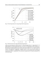
PL show in the high energy region, the maximum position is around 3.00 eV for all
composition, but the emission band is a broad band composed by two bands, at 2.98eV
(414nm) and 3.03eV (408 nm) (Figure 9). PL lower energy region for PSZTC and PLZTN
samples show the band at 1.87 eV (659 nm), additionally is observed that band at 1.74 eV is
not present in all compositions and its intensity is reduced appreciably with the
incorporation of Cr (Durruthy et al, 2010a, , 2011).
The general effect of the Cr doping is a decrement the PL intensity in both region bands with
the increase of dopant. It is noted that the PL of doped La
3+
and Nb
5+
is larger than of
undoped samples and increased with the composition of both ions at least one order of
magnitude for PSZTC, but is two and three order to PZTN and PLZT respectively.
It was of waiting that doped La
3+
and Nb
5+
increase PL intensity in 1.87 eV (659 nm) in PL, it
is well known that is associated with lead vacancies, due to the compensation of charge, in
this case the disorder or lead vacancy should be associated to the substitution of La
3+
by Pb
2+
in the host structure and the typical presence of lead vacancy due to the sintering route
(Calderón-Piñar et al, 2007; Silva et al., 2005). The presence of the peak at 1.87 eV, in PSZTC
0.2-0.5 mol % and PLZTN 1 mol% indicates a common defect related with a deep level
inside the band gap. As we saw in the region of high energy (3.00 eV) results are similar to
showed above previously.
The peaks that appear in zone (2.65) was associated with oxygen vacancies, simple or
double ionized. In the sample PLZTN evidently that E
D
will be ≥ 0.54 eV, and E
PL
is lower
2.43-2.74. This is because E
D
is not exactly one unique value because there are a distribution
defects in the structure.
The analysis of the peak at 1.86 eV could be associated to the simultaneous presence of
oxygen and lead vacancies (Guiffard et al, 2005; Durruthy et al, 2010a, b, 2011). The PL
response in the donor-acceptor mechanism in this case between the levels associated to the
oxygen near and below conduction band and the level of lead vacancies above the valence
band. Analogously the theoretical quantum mechanical calculation reported by de Lazaro
et al. (2007) justify that the presence of disorder associated to the substitution of Zr/Ti or
displacement of the ions in the B sites produce an amorphous zone in the ceramic with a
direct band gap with a separation near to 1.87eV. Beside this, we are detecting some small
peaks whose energy is around of 2.00-2.80 eV which belong to the visible energy spectra
too (Figure 9).
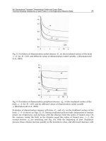
The calculated results of the band gap values for the PSZTC samples sintered at 1250 ºC are
summarized in Table 2. The figure 11 allows us to affirm that the dependence with Zr/Ti
ratio is very strong, and has a maximum in the morphotropic phase boundary and the
lowest values are for the composition 80/20, this behavior coincides with the calculations
Ferroelectrics – Physical Effects
630
carried out by J. Baedi et al. (2008). Figure 12 shows the way that would be materialize
recombination in the PSZTC and PLZTN samples. We supposed that the main way was 1, 5
and 6 for the experimental results obtained, in this work.
Fig. 9. Room temperature PL emission spectra for PSZTC and PLZTN ceramics at different
dopant concentration, fixing exited band at 373 nm.
Fig. 10. PL emission spectra at room temperature for PSZTC fixing exciting at 412 nm.
Photoluminescence in Doped PZTFerroelectric Ceramic System
631
PSZTC PLZTN
mole %
E
g
a
p
mole %
E
g
a
p
0.0 3.25 0.0 3.15
0.1 3.33 0.2 -
0.2 3.35 0.4 2.88
0.3 3.36 0.6 2.91
0.4 3.36 0.8 3.07
0.5 3.32 1.0 2.50
Table 2. Band gap energy (Eg) for PZT soft and hard, determined using the diffuse
reflectance principle (Kubelka-Munk expression). Error Eg= ± 0.003 eV. For E
PL
supposed
E
D
=0.54.
Fig. 11. Behavior of the forbidden band energy for PSZTC and PZTN ceramics, which agrees
with the results obtained for J. Baedi et al. (2008)
Fig. 12. Possible energetic process that will be happen in PZT ceramics. 3.4 eV is excitation
energy (373 nm), 1-6 there are the possible recombination way (PL). We consider that
occurred the way 1, 5 and 6 mainly.
0.5 eV
Ferroelectrics – Physical Effects
632
3. Dielectric characteristic
Another characteristics of these materials that they are very affected by the presence of
oxygen vacancies there are dielectric (ε) and loss (tan δ), for this we present some results in
different substitution type in ABO
3
perovskite structure.
The dielectric curves reveal anomalies in the neighbor at transition temperatures
corresponding to F
R(HT)
– P
C
(T
C
) and F
T
– P
C
(T
F-P
) phase transitions. Strong influence of
dopant La, Nb and La+Nb on the phase transition temperature (T
C
) is confirmed. The
comparison of ε(T) curves, obtained for the ceramic samples is shown in Figure 13, dielectric
measurement shows a decreasing T
C
and T
F-P
when increasing the dopant concentration.
The dielectric permittivity decreases for dopant concentration larger than 0.8 mol% (Figure
13), in particularity in Nb-doped ceramics permittivity decreases for concentrations up to
about 0.8 mol %, and then it increases slightly, as the grain size behaves. The same as in PL,
the permittivity is more intense for substitutions in B and A+B, in this case it is 4 times.
There is good agreement between the transition temperatures obtained from ε and tgδ,
respectively, considering the range of measurement error (δt ~ 5 °C), for almost every
sample. Those compositions with 0.6 and 1.0 % La have T tgδ
max
at 50 kHz differing 7.3-8.2
o
C from the value obtained at 1 kHz. A possible cause of such differs is the presence of
inhomogeneities as a result of compositional fluctuations (Gupta & Viehland, 1998; Garcia et
al., 2001).
In those samples doped with La+Nb, there is not a sum of the separate effects of La and Nb.
Note that temperatures are not as low as those for Nb, but compared to those for La they are
50 °C below.
Fig. 13. Permitivity as a function of temperature, measured at various frequencies, for PZT
53/47 ceramics showing La
2
O
3
, Nb
2
O
5
, and Nb
2
O
5
+La
2
O
3
content.
Photoluminescence in Doped PZTFerroelectric Ceramic System
633
Grain size decrement implies domain size decrement (Figure 14). Thus, the domain walls
become more movable, so the mechanical friction is small, and then the samples doped with
Nb and La+Nb are more compositionally homogenous (the evidence is given by narrow
plots of dielectric permittivity vs. temperature, that is, increasing permittivity). On the other
hand, grain size increment contributes to higher values of the dielectric constant, as a
measurement of the number of polarized unitary cells. The amount of polarization of such
cells is related to the presence of Nb
5+
and La
3+
inside the cristalline structure and
contributes to the orientation of the domain walls. An increasing dopant concentration
produces the increment of the number of lead vacancies and so the dielectric permittivity
grows. The values of ε for PZTN samples are higher and attributed to the higher
compositional homogeneity and the existence of only one phase in this composition. But is
not the same for PLZTN and PLZT, XRD patterns of samples show the tetragonal and
rhombohedral PZT phases together. (Figure 15) in all doped samples, with concentration
near to MPB (53/47).
Decrements of Tc might be attributed to the integration of dopants into the cristalline
structure.
Fig. 14. SEM results for 0.6, 0.8 and 1.0 mol % dopant in study for samples near to MPB.
In every case, the decrement of grain size as the dopant concentration increases is
observed.
Ferroelectrics – Physical Effects
634
20 30 40 50 60
(121)
R
(-121)
R
(-211)
T
(112)
T
(211)
T
(102)
T
(201)
T
(210)
T
(-120)
R
(120)
R
(002)
T
(200)
T
(020)
R
(111)
T
(-111)
R
(111)
R
(-110+110)
R
(110+101)
T
(001)
T
(100)
T
(010)
R
Pb
1-3x/2
A
x
(Zr
0.53
Ti
0.47
)
1-y
B
y
O
3
PZT
PLZTN
PZTN
Intensity (a.u.)
2θ Grade
PLZT
Fig. 15. Room temperature DRX patterns for PZT, PLZT, PZTN and PLZTN 53/47/1.0
sinter ceramics. Note for PZTN there are more tetragonal phase, observe better resolution of
002/200 plane.
To determine the factor most influential in dielectric permittivity behaviour with the dopant
concentration, the influence of porosity was analyzed. As it was seen in Table 3 it varies in
an appreciable way (~ 14%) in the studied composition interval.
Among the models proposed to evaluate the properties of porous materials, applicable to
systems with inferior porosity values at 0.6, it (the model) stands out the Bruggeman model.
This model offers a satisfactory description of the properties of piezoelectric porous ceramic,
in particular those based on PZT. A detailed explanation can it turns in works from Wersing
et al (1986).
The model establishes a peculiar relationship between experimental permittivity [ε(p0)] and
the theoretical [εpo=0], through of porosity fraction (p0) given by the equation (5),
considering connectivity (3-0).
ε(p
o
)= ε p
o=0
*(1- p
o
2/3
) (5)
Table 3 shows the results for the dielectric permittivity theoretical and experimental at room
temperature. A marked difference exists among both, being bigger for the Nb and the
La+Nb, what indicates the influence of this impurity in the evolution of the porosity, also
Δε to diminish with the frequency
Photoluminescence in Doped PZTFerroelectric Ceramic System
635
Niobio
Frecuencia
kHz
0,2 1,0
ε(
Po
) ε
Po=0
Δε
ε(
Po
) ε
Po=0
Δε
0,5 830 1249 419 1373 1669 296
1 635 955 320 1335 1646 292
5 587 883 296 1307 1589 282
10 482 725 243 1297 1577 280
25 251 378 127 1269 1543 274
Lantano
0,6 1,0
0,5 343 395 52 566 658 92
1 286 329 43 549 638 89
5 155 180 25 425 494 69
10 128 148 20 304 354 50
25 109 126 17 160 186 26
Lantano+Niobio
0,4 1,0
0,5 343 588 245 784 1035 251
1 286 491 205 768 1015 247
5 155 204 49 734 970 236
10 128 220 92 710 934 224
25 109 187 78 654 864 210
Table 3. Theoretical and experimental permittivity and their difference at room temperature
for 5 frequencies, for PZTN, PLZT and PLZTN 53/47/y ceramic, based on the Bruggeman
model.
It is important to make notice that this model considers a materials as a not homogeneous
médium and it start with two components: material and pores. In the material component
there are all that is not pore, that doesn't have to be necessarily homogeneous, due to the
procedure method.
The porosity is not the only factor that determines the permittivity variation with dopant
concentration. The analysis for dopant type shows that to smaller concentration bigger
porosity, but also bigger grain size, therefore is this last one the most influential in the
variations of the dielectric parameter. For example, 0.6% of Nb, the smallest difference exists
among the theoretical and experimental results, and the porosity has the fundamental rol,
for this concentration "po" it is minimized; in the other concentrations exists a cooperative
effect of the porosity and the grain size (Sundar et al. 1996), noted how for 1.0% "po" slightly
increases the grain size and Δε (Table 3). In La3+ case, Δε diminishes with the frequency and
increases with dopant concentration (Table 3), but ε is increasing with grain size decrement,
therefore both factors will contribute in a cooperative way in the relative permittivity
(Figure 16). The samples doped with La+Nb have a grain size between 1 and 2 microns, in
Ferroelectrics – Physical Effects
636
addition the contribution of the porosity is strong in the behavior of dielectric permittivity,
being greater even for the composition 0.8. The factors that determined the variation of the
permittivity with increasing dopant concentration are the grain size (Cancarevic et al., 2006)
and porosity, fundamentally.
Fig. 16. Behavior at room temperature of dielectric constant () and porosity (po) as
function of the grain size.
4. Conclusion
The used of PL and diffuse reflectance measurement in polycrystalline ceramics to
determine the band gap and the mechanism of the recombination in samples is possible. The
experimental results agree with those calculated.
All system present show mainly two region of emission bands around 1.8 and 3 eV, the
presence of broad band (1.8 eV) at the band gap can be associated to the vacancy defect
common in all (containing lead) ceramics sintered at high temperatures, the emission at
around 3eV correspond to direct recombination from CB to VB .
The emission at 2.56 eV, this present but it is not very intense in all the analyzed materials.
Shows the highest intensity and a shift to higher energies in the tetragonal phases. The Nb
concentration produces appreciably intensity changes and is associated to a transition from
oxygen vacancy levels to valence band. PZTN presents the biggest intensity in this band,
what indicates that the oxygen vacancy concentration is higher than lead vacancies.
But not all the dopant has same behavior, in all zone of PL spectra Cr diminish PL intensity
with increase concentration, while La
3+
, Nb
5+
and La
3+
+Nb
5+
increase PL intensity with the
increase dopant concentration.
Another interesting aspect is that A+B doped produces an increment to 2-3 order in PL
intensity, principally for “soft” doped.
110100
400
800
1200
1600
2000
ε Nb
ε La
ε La+Nb
ε
Grain size, μm
110100
0,05
0,10
0,15
0,20
0,25
0,30
po
po
Nb
po
La
po
La+Nb
Photoluminescence in Doped PZTFerroelectric Ceramic System
637
On the other hand, a strong influence of dopants on the decrement of grain size as
concentration grows is observed. The substitution in the A place and the simultaneous
substitutions in the A and B places provokes mixture of (tetragonal and rombohedral)
phases, while substitution in the B place the structure is tetragonal at least in 95 %. A texture
effect is also noticed, as it grows with the dopant concentration.
XRD results are confirmed by the obtained dielectric characteristics. In the PLZT, PLZTN
and PSZTC samples which present phase mixture, two peaks in the 1/ε curves are observed
and associated to Ferro-Ferro (rombohedral-tetragonal) and Ferro-Para (tetragonal-cubic)
phase transitions. Substitutions in the B place contribute more significantly to the Curie
temperature drop, with a minimum for PZTN 0.8 %.
5. Acknowledgements
This work was supported by project PNCB 10/04, Cuba, Sabbatical program CONACYT,
Mexico. The author appreciate work of Ing. M. Hernandez, Ing. F. Melgarejo, Ing. M.
Landaverde and Ing. E. Urbina. And to Cybernetic, Mathematical and Physics Instituted.
6. Reference
Anicete-Santosa, M., Silva, M.S., Orhan, E., Gomes, M. S., Zaghete, M. A., Paiva-Santos, C.
O., Pizani, P. S., Cilense, M., Varela, J. A., Longo, E., (2007) Contribution of
structural order–disorder to the room-temperature photoluminescence of lead
zirconate titanate powders. Journal of Luminescence, Vol. 127, Issue 2, 689-695
Baedi, J., Hosseini, S.M., Kompany, A., (2008) The effect of excess titanium and crystal
symmetry on electronic properties of Pb(Zr1?xTix)O3 compounds. Computational
Materials Science, Vol: 43, Issue: 4, 909-916, ISSN: 09270256.
Bharadwaja, S.S.N., Saha, S., Bhattacharyya, S., Krupanidhi, S.B., (2002) Dielectric properties
of La-modified antiferroelectric PbZrO 3 thin films. Materials Science and
Engineering B vol 88, issue 1, 22-25, ISSN 0921-5107
Calderón-Piñar, F., Aguilar, J., García, O., Fuentes, J., Contreras, G., Durruthy-Rodríguez, M.
D., Peláiz-Barranco, A., (2007) Mediciones de fotoluminiscencia en sistema PLZT
para determinar su relación con los mecanismos de conducción. Mediciones
térmicas de materiales sinterizados tipo BSZT. Instituto de Cibernética, Matemática
y Física (I CIMAF) Research Report 2007-412, ISSN 0138-8916
Cancarevic, M., Zinkeivich, M., Aldinger, F., (2006) Thermodynamic Assessment Of The Pzt
System Journal Of The Ceramic Society Of Japan, Vol. 114, Issue:1335, 937-949,
ISSN 0914-5400
Chang, Q. Sun, Jin, D., Zhou, J., Li, S., Tay, B.K., Lau, S.P., Sun, X.W., Huang, H.T., Hing, P.,
(2001) Intense and stable blue-light emission of Pb(Zr
x
Ti
1-x
)O
3
. Applied Physics Letters
Vol 79, No. 6, 1082-1084, ISSN 1077-3118
Chen, J., Chan, H.M., Harmer, M., (1989) Ordering Structure and Dielectric Properties of
Undoped and La/Na-doped Pb(Mg1/3Nb2/3)O3. J. Am. Ceram. Soc. Vol. 72, No.
4, 593-598, ISSN 0002-7820
de Lazaro, S., Milanez, J., de Figueiredo, A.T., Longo. V.M., Mastelaro,V.R., de Vicente, F.S.,
Hernandes, A.C., Varela, J.A., Longo E., (2007) Relation between
Ferroelectrics – Physical Effects
638
photoluminescence emission and local order-disorder in the CaTiO3 lattice
modifier. Applied Physics Letters 90, 111904-1 - 111904-3, ISSN 0003-6951
Dixit, A., Majumder, S. B., Katiyar, R. S., Bhalla, A. S., (2006) Studies on the Relaxor Behavior
of Sol-Gel Derived Ba(ZrxTi1-x)O3 (0.30 ≤ x ≤ 0.70) Thin Films. Journal of Materials
Science 41, 87, ISSN 0022-2461
Durruthy, M. D., Fuentes, L., Hernandez, M., Camacho , H. (1999) Influence of the niobium
dopant concentration on the Pb(Zr0.54Ti0.46)O3 ceramics sintering and final
properties. Journal of Materials Science 34 2311 – 2317
Durruthy-Rodríguez, M.D., Hernández-García, M., Suárez- Gómez A. (2002) Lanthanum
and niobium doping on PZT ceramic synthesis. Revista CENIC Ciencias Químicas,
Vol. 33, No. 1, 29-33, ISSN 0254-0525
Durruthy-Rodríguez, M.D., Costa-Marrero, J., Hernández-García, M., Calderón-Piñar, F.,
Yañez-Limón, J.M. (2010a) Photoluminescence in “hard” and “soft” ferroelectric
ceramics. Applied Physics A, 98, 543–550, DOI 10.1007/s00339-009-5501-y
Durruthy-Rodríguez, M. D., Costa-Marrero, J., Hernández-Garcia, M., Calderón-Piñar, F.,
Malfatti, C., Yañez-Limón, J. M., Guerra, J. D. S. (2010b) Optical characterization in
Pb(Zr
1−x
Ti
x
)
1−y
Nb
y
O
3
ferroelectric ceramic system. Applied Physics A, DOI
10.1007/s00339-010-6017-1, ISSN 1432-0630
Durruthy-Rodríguez, M.D., Costa-Marrero, Calderón-Piñar, F., Yañez-Limón, J.M., Guerra ,
J. D. S., (2011) Photoluminescence in Pb0.95Sr0.05(Zr1-xTix)1-yCryO3 ferroelectric
ceramic system. Journal of Luminiscence (accepted), ISSN 0022-2313
Eyraud, L., Guiffard, B., Lebrun, L., Guyomar, D., (2006) Interpretation of the Softening
Effect in PZT Ceramics Near the Morphotropic Phase Boundary. Ferroelectrics Vol.
330, issue 1, 51-60, ISSN 0015-0193
Garcia, S., Font, R., Portelles, J., Quiñones, R.J., Heiras, J., Siqueiros, J.M. (2001) Effect of Nb
doping on (Sr,Ba) TiO3 (BST) ceramic samples. Journal of Electroceramics, Vol. 6,
No. 2, 101-108, ISSN 1385-3449
Ghasemifard M., Hosseini S.M., Khorsand Zak A., Khorrami Gh. H. (2009) Microstructural
and optical characterization of PZT nanopowder prepared at low temperature.
Physica E: Low-dimensional Systems and Nanostructures, Volume 41, Issue 3, 418-
422, ISSN 13869477
Guiffard, B., Boucher, E., Eyraud, L., Lebrun, L., Guyomar, D., (2005) Influence of donor co-
doping by niobium or fluorine on the conductivity of Mn doped and Mg doped
PZT ceramics. Journal of the European Ceramic Society, Volume 25, Issue 12, 2487-
2490, ISSN 0955-2219
Gupta, S.M., Viehland, D., (1998) Tetragonal to rhombohedric transformation in the lead
zirconium titanate lead magnesium niobate-lead titanate crystalline solution. J.
Appl. Phys., 83, 1407-414. ISSN 1089-7550
Haertling, G. H. Ferroelectric (1999) Ceramics: History and Technology. Journal of the
American Ceramic Society, Vol. 82, 4, 797–818, DOI:10.1111/j.1151-
2916.1999.tb01840.x
Jaffe, B., Roth, R.S., Marzullo, S. (1954) Piezoelectric Properties of Lead Zirconate‐Lead
Titanate Solid‐Solution Ceramics. Journal of Applied Physics, Volume 25, Issue 6,
809-810, ISSN 0021-8979
Photoluminescence in Doped PZTFerroelectric Ceramic System
639
Jaffe, B.; Cook, W.R; Jaffe, H., (1971) Piezoelectric Ceramics, Academic Press, London and
New York, ISBN 0 12-379550-8
Kottim G. (1969) Reflectance Spectroscopy, Springer Verlag, New York. ISBN 0 19 850778x
Lines, M. E., Glass, A. M., (2001) Principles and applications of ferroelectrics and related
materials, Oxford University Press Inc., New York.
Longo V. M., Cavalcante L. S., de Figueiredo A. T., Santos L. P. S., Longo E., Varela J. A.,
Sambrano J. R., Paskocimas C. A., De Vicente F. S. and Hernandes A. C. (2007)
Highly intense violet-blue light emission at room temperature in structurally
disordered SrZrO3 powders. Applied Physics Letters 90, 091906-1 - 091906-3. ISSN:
0003-6951
Longo, E., de Figueiredo, A.T., Silva, M.S., Longo, V.M., Mastelaro, V.R., Vieira, N.D.,
Cilense, M., Franco, R.W.A., Varela, J.A., (2008) Influence of Structural Disorder on
the Photoluminescence Emission of PZT Powders. J. Phys Chem A. 112, 8953-8957,
ISSN 1089-5639
Mansimenko Y.L., Glinchuk M.D., Bykov I.P. (1998) Photoinduced Centers in the Optically
Transparent PLZT(8/65/35) Ceramics. Jounal of the Korean Physical Society 32,
S1039-S1041, ISSN 0038-1098
Nakajima H., Mori, T., Itoh, S., Watanabe, M., (2004) Photoluminescence properties of trace
amounts of Pr and Tb in yttria-stabilized zirconia. Solid State Communications vol.
129, issue 7, 421-424
Noheda, B., Cox, D.E., Shirane, G., Guo, R., Jones, B., Cross, L.E., (2001) Stability of the
monoclinic phase in the ferroelectric perovskite Pb(Zr
1-x
Ti
x
)O
3
. Physical Review B
(Condensed Matter) 63, 014103-1, 1550-235X
Noheda, B., Gonzalo, J.A., Cross, L.E., Guo, R., Park, S.E., Cox, D.E., Shirane, G.,
(2000)Tetragonal-to-monoclinic phase transition in a ferroelectric perovskite: The
structure of Pb(Zr
0.52
Ti
0.48
)O
3
. Physical Review B 61, 8687-8695,
DOI:10.1103/PhysRevB.61.8687
Ronda C. (2008) Luminescence: From Theory to Applications. Edited by WILEY-VCH
Verlag GmbH & Co. KGaA, ISBN: 978-3-527-31402-7, Weinheim.
Shannigrahi, S.R., Tripathy, S. (2007) Micro-Raman spectroscopic investigation of rare earth-
modified lead zirconate titanate ceramics. Ceramics International vol. 33, n 4, 595-
600, ISSN 0272-8842
Silva, M.S., Cilense, M., Orhan, E., Gomes, M.S., Machado, M.A.C., Santos, L.P.S., Paiva-
Santos, C.O., Longo, E., Varela, J.A , Zaghete, M.A., Pizani, P.S., (2005)The nature of
the photoluminescence in amorphized PZT. Journal of Luminescence 111, 205–213,
DOI:10.1016/j.jlumin.2004.08.045
Sivasubramanian V., Kesavamoorthy R., Subramanian V. (2007) Photoluminescence
investigations on the nanoscale phase transition in Pb(Mg1/3Nb2/3)O3. Solid State
Communications Vol. 142, Issue 11, 651-654, ISSN 0038-1098
Suárez-Gómez, A., Durruthy, M. D., Costa-Marrero, J., Peláiz-Barranco, A., Calderón-Piñar,
F., Saniger-Blesa, J. M., de Frutos, J.(2009) Properties of the PLZTN x/54/46 (0.4 ≤ x
≤ 1.4) ceramic system. Materials Research Bulletin vol. 44, 1116–1121, ISSN 0025-
5408
Ferroelectrics – Physical Effects
640
Sundar, V., Kim, N., Randall, C.A., Yimnirun, R., Newnham, R.E. (1996) The effect of
Doping and grain size on Electrostriction in PbZr0.52 Ti0.48O3. IEEE, 1, 935-938,
ISBN 0-7803-3355-1
Tai, C.W. & Baba-Kishi, K.Z. (2002) Microtexture studies of PST and PZT ceramics and PZT thin
film by electron backscatter diffraction patterns. Textures and Microstructures, Vol. 35,
No. 2, 71–86, ISSN 1029-4961.
Wendlandt, W.W., Hecht, H.G (1966) Reflectance Spectroscopy, Wiley Interscience, New
York, BCIN Number 62796
Wersing W., Lubitz K., Mohaupt J. (1986) Dielectric, elastic and piezoelectric properties of
porous PZT ceramics. Ferroelectrics, 68, 77-79. ISSN 0015-0193
Yang, Z., Liu, Q H., (2008) The structural and optical properties of ZnO nanorods via citric
acid-assisted annealing route. Journal of Materials Science, Volume 43, Number 19,
6527-6530, ISSN 0022-2461
Yu, P.Y., Cardona, M., (1996) Fundamentals of semiconductors. Physics and Materials
Properties. Ed. Springer-Verlag, Berlin, ISBN 978-3-642-00710-1
28
Photovoltaic Effect in Ferroelectric
LiNbO
3
Single Crystal
Zhiqing Lu, Kun Zhao and Xiaoming Li
Laboratory of Optic Sensing and Detecting Technology, College of Science
People’s Republic of China
1. Introduction
Lithium niobate (LiNbO
3
) is a human-made dielectric material and was first discovered to
be ferroelectric in 1949. Properties and applications of LiNbO
3
have been widely studied,
resulted in several thousands of papers on this material, since the crystal was successfully
grown using the Czochralski method by Ballman in 1965 (Kong et al., 2005). It has been
extensively researched for its excellent ferroelectric, piezoelectric, dielectric, pyroelectric,
electric-optical and nonlinear optical properties (Wang et al., 2008; Chen et al., 2007; Sarkisov
et al., 2000). Now LiNbO
3
is a very significant material for optical applications, such as acoustic
wave transducers, acoustic delay lines, acoustic filters, optical amplitude modulators, optical
phase modulators, second-harmonic generators, Q-switches, beam deflectors, dielectric
waveguides, memory elements, holographic data processing devices, and others (Kim et al.,
2001; Zhen et al., 2003; Pham et al., 2005; Liu et al., 2002; Zhou et al., 2006).
LiNbO
3
is a ferroelectric material which has the highest Curie temperature of about 1210 °C
up to now and the largest spontaneous polarization of about 0.70 C/m
2
at room
temperature. LiNbO
3
single crystals exhibit paraelectric phases above the Curie temperature
and ferroelectric phases below the Curie temperature (Karapetyan et al., 2006; Bermúdez et
al., 1996). Ferroelectric LiNbO
3
crystal is a member of the trigonal crystal system, exhibiting
three-fold rotation symmetry about its c axis. Its structure consists of planar sheets of
oxygen atoms in a distorted hexagonal close-packed configuration. The octahedral
interstices in this structure are one-third filled by lithium atoms, one-third by niobium
atoms, and one-third vacant. In the paraelectric phase the Li atoms and the Nb atoms are
centered in an oxygen layer and an oxygen octahedral, making the paralelctric phase non-
polar. But in ferroelectric phase the Li atoms and the Nb atoms shifted into new positions
along the c axis by the elastric forces of the crystal, making the LiNbO
3
crystal exhibiting
spontaneous polarization (Bergman et al., 1968).
Many methods were reported to determine the +c axis of ferroelectric LiNbO
3
single crystal.
A standard method is to compress the crystal in the c axis direction. The +c axis is defined as
being directed out of the c face that becomes negative upon compression. This can be
understood that the Li and Nb ions move closer to their centered positions upon
compression, leaving excess negative compensation charges on the +c face, causing the +c
face to become negative. Anther method to identify the +c face and –c face of the crystal is
an etching technique with HF solution. The etching speed on the –c face is faster than on the
+c face (Beghoul et al., 2008; Bourim et al., 2006). Other methods to determine the +c axis
Ferroelectrics – Physical Effects
642
were also reported such as to cool the crystal, observation of the terraces on a cleavage
plane, x-ray diffraction techniques (Boyd et al.,1964; Kaminow et al., 1980).
In the past few years, various types of photodetectors were proposed, such as
photoconductor, Schottky barrier detector, p-i-n junction photodiode, and heterogeneity
junction (Wang et al., 2007; Jin et al., 2007). Photovoltaic effect plays an important role in the
investigation of these photodetectors. Photovoltaic effects in LiNbO
3
crystals were observed
by Chen in 1969 (Chen, 1969). Then LiNbO
3
was found to be in response to ultraviolet,
visible, and infrared radiation of laser (Dai et al., 2005). LiNbO
3
is a promising material for
photodetector because of its high responsibility, good dielectric properties, and low cost. For
example, ultraviolet photodetectors have attracted a strong interest owing to their broad
potential applications in the fields of automatization, short-range communications security,
biological researches, and military services. The band gap of LiNbO
3
single crystal is ~ 4 eV,
which can be suggested as a promising material for UV photodetector since the present
ultraviolet photodetectors based on various wide band gap semiconductors, such as III–V
nitrides, silicon carbide, zincoxide, and diamond, require a complicated fabrication process
and high-cost manufacturing (Razeghi & Rogalski, 1996; Topic et al., 2001; Tomm
et al., 2000; Spaziani et al., 2003). In this chapter, photovoltaic effect in pure congruent
LiNbO
3
single crystals will be introduced, including vertical photovoltaic effect, lateral
photovoltaic effect and photovoltaic effects in miscut LiNbO
3
single crystals (Lu et al., 2009;
Li et al.,2010).
2. Photovoltaic effects in LiNbO
3
single crystal
2.1 Vertical photovoltaic effects
Commercial optical grade z-cut LiNbO
3
single crystal was used in the experiment, which
was double polished with a dimension of 5×5×0.5 (mm) in the a, b, and c directions,
respectively. The two silver paste electrodes were placed on the opposite two surfaces of the
crystal respectively. An actively/passively mode locked Nd:yttrium-aluminum-garnet
(Nd:YAG) laser (with pulse duration of 25 ps, repetition rate of 10 Hz) was used to irradiate
the sample at the wavelengths of 1064, 532, and 355 nm at room temperature. The laser
beam was directed onto the sample near to the electrode and passed through the crystal
along the c axis, as shown in the inset in Fig.1. The diameter of the spot was 2 mm. The open
circuit photovoltage were measured and recorded by a digital storage oscilloscope. Figure 1
presents the typical ultrafast photovoltaic signals observed under the pulsed laser of three
different wavelengths. The laser pulse energy of 355, 532 and 1064 nm is 0.56, 0.60 and 0.58
mJ respectively .We can see that the response time is about 2 ns and the full width at half
maximum (FWHM) is about 1.8 ns.
All the photovoltages measured by the oscilloscope were negative whether the laser pulse
irradiated on the top surface or on the bottom surface of the crystal, shown in Fig.1. It has
been known that the ferroelectric LiNbO
3
exhibits spontaneous polarization below its Curie
temperatures, which direction is from –c face to +c face of the crystal (Wemple et al., 1968).
So there is a built-in electric field in LiNbO
3
crystal in the direction from the positive end of
spontaneous polarization to the negative end, antiparallel to the spontaneous polarization.
Here we identified the –c face and +c face using an etching technique with HF solution of
40%. When the laser spot directed on the crystal, photo-excited electrons drifted toward the
positive end of spontaneous polarization under the influence of the internal electric field,
undergoing the course of excited-captured-reexcited-recaptured before they eventually
Photovoltaic Effect in Ferroelectric LiNbO
3
Single Crystal
643
drifted to the
+
c face. So we always get a negative signal on the oscilloscope whether the
laser irradiated on the
+
c face or on the –c face.
Fig. 1. Typical ultrafast photovoltage with time when the sample irradiated by pulsed laser
of three different wavelengths. The solid line is the signal when irradiated on the +c face of
the crystal and the short dash line is on the –c face. All the signals measured are negative.
The peak voltage values of open circuit verse the pulse energy has been also measured
under the irradiation of the three different wavelengths. The results are summarized in
Fig.2. We can see that the photovoltages under the three wavelengths increased linearly
with the incident energy of each laser pulse.
The photovoltage V that appears in the crystal is (Feng et al., 1990)
dph
J
Vl
σσ
=
+
(1)
where J is the photovoltaic current,
σ
d
and
σ
ph
are dark conductivity and photoconductivity
of the crystal, respectively, and l is the distance between the electrodes. Since
σ
d
(<10
-15
Ω
-
1
cm
-1
) is much smaller than
σ
ph
, we can neglect it.
Ferroelectrics – Physical Effects
644
Fig. 2. The peak open-circuit photovoltage as a function of the energy of pulsed laser. The
photovoltage is proportional to the intensity of incident laser of 355, 532 and 1064 nm,
respectively.
The photovoltaic current of LiNbO
3
crystal is given by (Glass et al., 1974)
ph
dn
JI EeD
dz
κα σ
=+ +
(2)
where
κ
is the glass coefficient,
α
is the absorption coefficient, I is the intensity of the
irradiated laser beam, E is the total electric field in the crystal, D is the diffusion coefficient,
and n is the carrier concentration. The first term represents the photovoltaic current, the
second term represents the drift current, and the third term represents the non-uniform laser
irradiation in the sample.
The photoconductivity is given by (Nakamura et al., 2008)
ph
h
I
e
α
σ
τμ
ν
=
(3)
where τ is the lifetime of an excited carrier in the conduction band,
μ
is the mobility, and h
ν
is the photon energy.
The carrier concentration n should be proportional to the intensity of the laser due to the
photoelectric effect. So the photovoltage V is proportional to the intensity of incident laser I,
as shown in Fig.2.
Continuous-wave (CW) laser of 532 and 1064 nm were also used to irradiate on the sample.
Negative photovoltage signal was also observed in the experiment, as shown in Fig.3. This is
in agreement with the results of the experiments above using pulsed lasers in Fig.1. The
reason is the existence of the spontaneous polarization and the internal electric field in the
crystal. When the power of the incident laser was changed from 0.6 to 60.4 mW, we found
that the peak photovoltages also increased linearly, as shown in Fig.4.
Photovoltaic Effect in Ferroelectric LiNbO
3
Single Crystal
645
Fig. 3. The negative photovoltages under the irradiation of continuous-wave laser of 532 and
1064 nm.
Fig. 4. The open-circuit photovoltages increased linearly with the intensity of the CW laser.
Defects in LiNbO
3
crystal are the main reason of the photovoltaic effect and the charge
transport.
There is at least about 1 mol % of intrinsic defects such as bipolarons and small
Ferroelectrics – Physical Effects
646
polarons in pure
congruent LiNbO
3
crystal (Schirmer et al., 2005). The absorption spectra of
LiNbO
3
(Fig.5) shows that the absorption peak of the sample is about at 310 nm, and there is
a common absorption peak of bipolarons and small polarons at 628 nm. So the transition
and migration of the electrons in LiNbO
3
crystal is mainly between the defects and the
conduction band.
Fig. 5. The absorption spectra of LiNbO
3
which shows two absorption peaks of the sample
that one is for band to band absorption and another is the common absorption peak of
bipolarons and small polarons.
On the basis of two-center model, for pure LiNbO
3
, the deep center is dominated by
bipolarons and the shallow center is governed by the small polarons. By laser pulses these
bipolarons can be dissociated at room temperature and released photo-excited electrons to
the conduction band. But the amount of the shallow center is very small in pure LiNbO
3
.
The energy between the deep center and the conduction band is about 2.0~2.5 eV. The
photon energy of 355 nm is 3.5 eV. So when the sample was irradiated by the laser of 355
nm, a large amount of electrons in deep center can be excited into the conduction band. The
photon energy of 532 nm is 2.3 eV, which is near to the energy between the deep center and
the conduction band, so it can excited part of electrons in deep center. Therefore, the peak
value of photovoltage of 355 nm is larger than that of 532 nm, as shown in Fig.2. The photon
energy of 1064 nm is 1.2 eV, which can not excite the electrons in deep center. But the deep
center can be dissociated not only by illumination but also heating. The temperature of the
crystal increased during the irradiation of 1064 nm laser in the experiment, and the deep
center is dissociated and released electrons. With the increase of the intensity of the incident
laser, the transition between the deep center and the shallow center should be taken into
account, for the dissociated energy of bipolarons is about 0.27 eV (Kong et al., 2005) .
2.2 Lateral photovoltaic effects
To investigate the lateral photovoltage in LiNbO
3
single crystal, two silver paste electrodes
were separated about 1.5 mm on the surface perpendicular to the c axis. The laser beam
passed through the crystal along the c axis and irradiated normally at the back of one
electrode, as shown in Fig. 6.
Photovoltaic Effect in Ferroelectric LiNbO
3
Single Crystal
647
Fig. 6. Schematic of measurement for sample irradiated by laser through (a) −c face (mode 1)
and (b) +c face (mode 2).
Typical ultrafast signals can be observed as shown in Fig. 7, with the rise time of about 1.5
ns and the FWHM of 1−2 ns. For mode 1, the signals were negative and positive when the
laser pulse irradiated the positive and negative electrodes, respectively (Fig. 6(a)). While the
reverse signals were recorded for mode 2 (Fig. 6(b)).
Due to inhomogeneous illumination in LiNbO
3
crystal, the concentration of photoelectrons
is larger in the illumination region than in the dark region. And the photoelectrons will drift
toward the +c face of the crystal because of the existence of a permanent electric field in the
direction from −c to +c faces, then diffuse toward another electrode. Thus we can get the
negative (positive) signals when the sample is irradiated at the back of positive electrode for
mode 1 (mode 2). The same results can be also obtained when the CW laser is used to
irradiate the crystal, as shown in Fig. 8. The dependence of the peak open-circuit
photovoltages on the incident light intensity is studied experimentally. The results are
summarized in Fig. 9. We can see that the photovoltages increase linearly with the laser
intensity, which can be well explained by the photovoltaic effects in LiNbO
3
crystal.
Fig. 7. Typical ultrafast photovoltages recorded for (a) mode 1 and (b) mode 2. Solid and
short dot lines are for the signals when the laser pulse irradiates the positive and negative
electrodes, respectively.
Ferroelectrics – Physical Effects
648
Fig. 8. Photovoltages for (a) mode 1 and (b) mode 2 under the irradiation of CW laser of 532
and 1064 nm. Solid line and open circle point are for the signals when the laser pulse
irradiates the positive and negative electrodes, respectively.
Fig. 9. Peak open-circuit photovoltages as functions of pulsed laser energy (solid point) and
CW laser power densities (open point) for (a) mode 1 and (b) mode 2.
Photovoltaic Effect in Ferroelectric LiNbO
3
Single Crystal
649
2.3 Photovoltaic effects in miscut LiNbO
3
single crystals
A single polished commercial LiNbO
3
single crystal with c-axis oriented is used for the
photovoltaic studies. The sample geometry is 5×5 mm
2
with the thickness of 0.5 mm. The
crystalline orientation is 10° miscut from the exact (001) orientation, which is
characterized by x-ray diffraction with the usual θ-2θ scan using Cu Κα
1
and Κα
2
radiations. As shown in Fig. 10, the offset point is set as ω=α or 45°-α to satisfy Braggs
diffraction, where α is the miscut angle. The two peaks arise from the (006) and (0012)
plane of LiNbO
3
and are clearly apart for Κα
1
and Κα
2
radiations. The inset of Fig. 10
shows the UV–visible absorption spectrum of LiNbO
3
crystals as a function of the
wavelength. The sharp absorption edge is about 310 nm, corresponding to the optical
band gap of LiNbO
3
and indicating that UV light, e.g. 248 nm laser, can generate electron–
hole carriers in LiNbO
3
crystals.
Fig. 10. The x-ray diffraction pattern of a miscut LiNbO
3
single crystal. The left inset shows
the absorption spectrum of LiNbO
3
single crystal. The right inset shows the configuration of
θ-2θ scan, where α is the miscut angle and ω the offset point.
The photovoltaic properties are investigated under the illuminations of a KrF pulsed laser
with the wavelength of 248 nm with 20 ns duration at a 10 Hz repetition. In order to study
the influence of the thickness on the photovoltaic effect, the samples are polished
mechanically into seven different thicknesses, which are 0.49, 0.45, 0.38, 0.28, 0.22, 0.17 and
0.09 mm, respectively. Before the photovoltaic measurements, the sample is cleaned by
using an ultrasonic cleaner in alcohol and acetone under routine cleaning process. Two
colloidal silver electrodes of about 1×5 mm
2
area, separated by 3 mm, are prepared on the
mirror polished surface of the LiNbO
3
single crystal and the opposite surface is exposed
wholly to the laser irradiation, as shown in the inset of Fig. 11. The photovoltaic signals are
recorded by using a sampling oscilloscope terminating into 50 Ω at room temperature. All
the measurements are carried out in the room temperature without any applied bias.
Typical voltage transients of the LiNbO
3
single crystal of different thicknesses to a pulsed
laser illumination are presented in Fig. 11. The peak photovoltage as a function of the
sample thicknesses is shown in Fig. 12, and the energies on the sample are 15.2 and 19.4 mJ,
Ferroelectrics – Physical Effects
650
respectively. With the decrease of the crystal thickness from 0.49 to 0.09 mm, the peak
photovoltage increases rapidly at first and then descendes. The maximum peak
photovoltage occurs at the thickness of 0.38 mm and reaches 35.6 and 31.1 mV for 19.4 and
15.2 mJ, with the corresponding photovoltaic sensitivities of 1.83 and 2.04 mV/mJ, which is
several times larger than that at 0.49 and 0.09 mm. In addition, the peak photovoltage is
found to depend linearly on the on-sample energy from 13.5 to 20.9 mJ for selected crystal
thicknesses of 0.22 and 0.09 mm, respectively, as shown in Fig. 13.
Fig. 11. The photovoltaic pulses for miscut LiNbO
3
single crystal under the illumination of a
248 nm laser for seven different thicknesses recorded by an oscilloscope with an input
impedance of 50 Ω at room temperature without any applied bias. The on-sample energy
was 15.2 mJ. The inset displays the schematic circuit of the measurement.
Fig. 12. The peak photovoltage dependence of the miscut LiNbO
3
single crystal thickness.
Photovoltaic Effect in Ferroelectric LiNbO
3
Single Crystal
651
Fig. 13. The peak photovoltage of the miscut LiNbO
3
single crystal as a function of on-
sample energy.
Figure 14 shows the 10%–90% rise time and FWHM as functions of the sample thickness for
the on sample-energy of 15.2 and 19.4 mJ, respectively. With the decrease of sample
thickness, the carriers reaches the two colloidal electrodes faster for thinner sample so that
faster photovoltaic response can be observed. The rise time descends obviously from 11.83
ns at 0.49 mm to 3.946 ns at 0.09 mm, suggesting that decreasing the sample thickness is a
useful way to obtain faster response detection. Since the miscut LiNbO
3
single crystal
Fig. 14. The rise time and FWHM as functions of the sample thickness.
Ferroelectrics – Physical Effects
652
Fig. 15. The schematic diagram of the transporting photogenerated carriers, indicating that
the carriers were separated and assembled at the two Ag electrodes by the SPEF.
exhibits an optical response time of ~ns, it can be applied to detect the present laser pulse,
which is further confirmed in Fig. 14, where the FWHM is independent of crystal thickness
and almost keeps a constant of ~20 ns in accord with the 248 nm laser duration.
It is well known that pure congruent LiNbO
3
is a spontaneous polarisation crystal and there
exists a spontaneous polarisation electric field (SPEF) along the c axis. In the experiment, the
crystalline orientation is 10° miscut from the exact (001) orientation, so is SPEF as shown in
Fig. 15 Under the 248 nm laser irradiation, photo-induced carriers are separated and
assembled at the two electrodes by the SPEF. Only those carriers reaching to the electrodes
in the back can be collected and give rise to photovoltaic signals. With decrease of crystal
thickness the amount of carriers collected by electrodes in the back increases due to lower
loss, which is resulted from the shorter transport distances as well as less traps and
recombination in thinner samples. Thus the signals for thinner samples are much larger than
that for thicker samples. On the other hand, the decrease of thickness also leads to decrease
of autologous carriers in LiNbO
3
single crystals, which limits the amount of carriers
collected by electrodes. The competition between the two above factors results into a
maximum photovoltaic signal at an optimum thickness at 0.38 mm.
3. Conclusion
The characteristics of the photovoltaic effect in LiNbO
3
single crystals were presented in
detail in this chapter. Vertical and lateral photovoltaic effects in pure congruent LiNbO
3
crystals were observed by using pulsed and continuous wave lasers with inhomogeneous
irradiation, respectively. The typical ultrafast response time and FWHM were about 2ns for
the open-circuit photovoltaic pulse, indicating the potential applications of LiNbO
3
single
crystal as photoelectronic detector. The thickness dependence of the photovoltaic effect in
miscut LiNbO
3
single crystal was also investigated. With the decrease of the crystal
thickness, the photovoltaic response time decreased monotonically, the photovoltaic
sensitivity is improved rapidly at first, and then decreases. The experimental results show
that decreasing the crystal thickness is an effective method for obtaining faster response
time and improving the photovoltaic sensitivity in single crystals.
Photovoltaic Effect in Ferroelectric LiNbO
3
Single Crystal
653
4. Acknowledge
This work was supported by the Program for NCET, NSFC, RFDP, Beijing Natural Science
Foundation, Foresight Fund Program from China University of Petroleum (Beijing).
5. References
Kong Y. F.; Xu J. J.; Zhang G. Y.; Liu S. M. & Lu Y. (2005), Multifunctional photoelectric
material: LiNbO
3
crystals. Science Press, ISBN 7-03-013660-8, Beijing
Wang, K.; Li, J. F. & Liu, N. (2008). Piezoelectric properties of low-temperature sintered Li-
modified (Na, K)NbO
3
lead-free ceramics. Appl. Phys. Lett., 93, 092904
Chen, J.; Li, Y. D.; Lu, W. Q.; Qi, J. W.; Cui, G. X.; Liu, H. B.; Xu, J. J. & Sun, Q. (2007).
Observation of surface-plasmon-polariton transmission through a silver film
sputtered on a photorefractive substrate. J. Appl. Phys., 102, 113109
Sarkisov, S. S.; Curley,M. J.; Williams,E. K.; Ila,D.; Svetchnikov,V. L.; Zandbergen,H. W.;
Zykov, G. A.; Banks,C.; Wang, J. C.; Poker, D. B. & Hensley, D. K. (2000). Nonlinear
optical waveguides produced by MeV ion implantation in LiNbO
3
. Nuclear
Instruments and Methods in Physics Research Section B: Beam Interactions with Materials
and Atoms, 166-167, 750-757
Kim, R. H.; Park, H. H. & Joo, G. T. (2001). The growth of LiNbO
3
(006) on MgO (001) and
LiTaO
3
(012) substrates by sol-gel procedure. Appl. Surf. Sci., 169-170, 564–569
Zhen, X. H.; Zhang, X. J.; Zhao, L. C. & Xu, Y. H. (2003). Growth and optical properties of
In:Nd:LiNbO
3
crystals. Solid State Commun.s, 126, 203-206
Pham, V. T.; Lee, S. K.; Trinh, M. T.; Lim, K. S.; Hamilton, D.S. & Polgár, K. (2005).
Nonvolatile two-color holographic recording in Tm-doped near-stoichiometric
LiNbO
3
. Opt. Commun.s, 248, 89-96
Liu, Y.; Kitamura, K.; Takekawa, S.; Ravi, G. & Nakamura, M. (2002). Nonvolatile two-color
holography in Mn-doped near-stoichiometric lithium niobate. Appl. Phys. Lett., 81,
2686-2688
Zhou, Q. F.; Cannata, J. & Shung, K. K. (2006). Design and modeling of inversion layer
ultrasonic transducers using LiNbO
3
single crystal . Ultrasonics, 44, e607-e611
Karapetyan, K. G.; Kteyan,A. A. & Vardanyan, R. A. (2006) Thermal reduction effect on
Curie temperature of LiNbO
3
ferroelectrics. Solid State Commun., 140, 474-476
Bermúdez, V.; Dutta, P. S.; Serrano, M. D. & Diéguez, E. (1996). In situ poling of LiNbO
3
bulk crystal below the Curie temperature by application of electric field after
growth. J. Crystal Growth, 169, 409-412
Bergman, J. G.; Askin, A.; Ballman, A. A.; Dziedzic, J. M.; Levinstein, H. J. & Smith, R. G.
(1968). Curie temperature, birefringence, and irefringence, and phase-matching
temperature variations in LiNbO
3
as a function of melt stoichiometry. Appl. Phys.
Lett., 12, 92-95
Beghoul, M. R.; Boudrioua, A.; Kremer, R.; Fontana, M. D.; Fougere, B.; Darraud, C.;
Vareille, J. C. & Moretti, P. (2008). Micro-Raman spectroscopy investigation of the
electron beam irradiation of LiNbO
3
surface for 2D photonic band gap grating
inscription. Opt. Mater., 31, 136-142
Bourim, E. M.; Moon, C. W.; Lee, S. W. & Yoo, I. K. (2006). Investigation of pyroelectric
electron emission from monodomain lithium niobate single crystals. Physica B,
383,171-182