Ferroelectrics Characterization and Modeling Part 5 docx
Bạn đang xem bản rút gọn của tài liệu. Xem và tải ngay bản đầy đủ của tài liệu tại đây (1.85 MB, 35 trang )
Ferroelectrics - Characterization and Modeling
130
using the Nye notation, in which elastic constants and elastic moduli are labeled by
replacing the pairs of letters xx, yy, zz, yz, zx, and xy by the number 1, 2, 3, 4, 5, and 6,
respectively. This means that the external electric field generates electric displacement, i.e.,
electric polarization, and strain through the converse piezoelectric effect.
However, ceramic materials are multicrystalline structures made up of large numbers of
randomly orientated crystal grains. The random orientation of the grains results in a net
cancelation of the piezoelectric effect. Thus, the ceramic material must be poled − a dc bias
electric field is applied (usually the fired ceramic piece is cooled through the Curie point
under the influence of the field) which aligns the ferroelectric domains, resulting in a net
piezoelectric effect.
As the electrical conductivity of percolative composites strongly increases on approaching
the percolation threshold, the feasibility of poling the PZT- Pb
2
Ru
2
O
6.5
samples has been
checked. PZT- Pb
2
Ru
2
O
6.5
system has been chosen as its electrical conductivity is much
lower than in the PMN-35PT–Pb
2
Ru
2
O
6.5
system or in the KNN–RuO
2
samples which are not
treated under vacuum. After poling the PZT-Pb
2
Ru
2
O
6.5
samples with a high dc bias electric
field, the piezoelectric coefficient d
33
(strain in the direction of the applied measuring field)
has been measured using a small ac voltage. It should be noted that, while various
piezoelectric coefficients are usually determined and thus the indication is absolutely
necessary, the dielectric constant is almost without exception determined in the direction of
the applied field, i.e., ε' without indices in fact denotes the dielectric constant ε
33
.
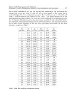
Results of piezoelectric characterization are shown in Fig. 12. While in samples, which are
very close to the percolation threshold, the breakdown electric field is below 5 kV/cm,
samples with lower Pb
2
Ru
2
O
6.5
content can be poled with the dc bias electric fields higher
than 30 kV/cm. It is thus once again revealed that percolative samples with compositions
near the percolation threshold are not very suitable for applications, while samples with
lower conductive filler concentration, where dielectric constant is still much higher than in
the pure ceramic matrix, are very promising for use as high dielectric constant materials.
0 5 10 15 20 25 30 35
0
10
20
30
40
50
60
10 vol. % of Pb
2
Ru
2
O
6.5
16.5 vol. %
15.5 vol. %
12.5 vol. %
d
33
(pC/N)
E
poling
(kV/cm)
PZT
−Pb
2
Ru
2
O
6.5
Fig. 12. Piezoelectric coefficient d
33
in various PZT-Pb
2
Ru
2
O
6.5
samples, measured with small
ac voltage, after poling the sample with a high dc bias electric field (E
poling
).
All-Ceramic Percolative Composites with a Colossal Dielectric Response
131
5. Conclusion
Development of all-ceramic percolative composites
i. PZT-Pb
2
Ru
2
O
6.5
ii. PMN-35PT–Pb
2
Ru
2
O
6.5
and
iii. KNN–RuO
2
based on the perovskite ferroelectric and ruthenium-based conductive ceramics is reported
in this chapter. The structural analysis revealed that there were no chemical reactions
between the constituents during processing, which resulted in a perfect structure of
composites – conductive ceramic grains are uniformly distributed throughout the
ferroelectric ceramic matrix. Thus, in the lead-based PZT-Pb
2
Ru
2
O
6.5
and PMN-35PT–
Pb
2
Ru
2
O
6.5
and in the lead-free KNN–RuO
2
systems the dielectric response in fact follows
the predictions of the percolation theory. As a result, the dielectric constant strongly
increases on the conductive filler increasing content, reaching values near the percolation
threshold that are for two orders of magnitude higher than in the pure matrix ceramics.
Furthermore, the determined critical exponents and percolation points agree reasonably
with the theoretically predicted values. The frequency- and temperature-dependent
dielectric response of all developed systems is also presented and discussed.
Finally, not only structural and dielectric results, i.e., a successful synthesis of lead-based
and lead-free percolative systems exhibiting a stable giant dielectric response, but also
electromechanical properties demonstrate the potential of all-ceramic percolative
composites for use as high-dielectric-constant materials in various applications.
6. Acknowledgment
This work was supported by the Slovenian Research Agency under project J1-9534 and
program P2-0105-0106/05 and under European project 6. FP NMP3-CT-2005-515757. We
thank to Prof. Horst Beige from the Martin-Luther University in Halle, Germany, for
kindly making the experimental facility for the electromechanical characterization of the
PZT–Pb
2
Ru
2
O
6.5
system accessible and to Dr. Ralf Steinhausen for help with these
measurements.
7. References
Bergman, D. J. & Imry, Y. (1977). Critical behavior of the complex dielectric constant near
the percolation threshold of a heterogeneous material. Physical Review Letters, Vol.
39, Iss. 19, Nov. 1977, pp. 1222-1225, ISSN 0031-9007.
Bobnar, V.; Hrovat, M.; Holc, J. & Kosec, M. (2008). Giant dielectric response in Pb(Zr,Ti)O
3
–
Pb
2
Ru
2
O
6.5
all-ceramic percolative composite. Applied Physics Letters, Vol. 92, Iss. 18,
May 2008, 182911 3pp., ISSN 0003-6951.
Bobnar, V.; Hrovat, M.; Holc, J.; Filipič, C.; Levstik, A. & Kosec, M. (2009a). Colossal
dielectric response in all-ceramic percolative composite 0.65Pb(Mg
1/3
Nb
2/3
)O
3
-
0.35PbTiO
3
-Pb
2
Ru
2
O
6.5
. Journal of Applied Physics, Vol. 105, Iss. 3, Feb. 2009, 034108
5pp., ISSN 0021-8979.
Bobnar, V.; Hrovat, M.; Holc, J. & Kosec, M. (2009b). All-ceramic lead-free percolative
composite with a colossal dielectric response. Journal of the European Ceramic Society,
Vol. 29, Iss. 4, Mar. 2009, pp. 725-729, ISSN 0955-2219.
Ferroelectrics - Characterization and Modeling
132
Chiteme, C.; McLachlan, D. S. & Sauti, G. (2007). ac and dc percolative conductivity of
magnetite-cellulose acetate composites. Physical Review B, Vol. 75, Iss. 9, Mar. 2007,
094202 13pp., ISSN 1098-0121.
Colla, E. V.; Yushin, N. K. & Viehland, D. (1998). Dielectric properties of (PMN)
(1 – x)
(PT)
x
single crystals for various electrical and thermal histories. Journal of Applied Physics,
Vol. 83, Iss. 6, Mar. 1998, pp. 3298-3304, ISSN 0021-8979.
Dang, Z M.; Lin, Y H. & Nan, C W. (2003). Novel ferroelectric polymer composites with
high dielectric constants. Advanced Materials, Vol. 15, Iss. 19, Oct. 2003, pp. 1625-
1629, ISSN 0935-9648.
Deepa, K. S.; Sebastian, M. T. & James, J. (2007). Effect of interparticle distance and
interfacial area on the properties of insulator-conductor composites. Applied Physics
Letters, Vol. 91, Iss. 20, Nov. 2007, 202904 3pp., ISSN 0003-6951.
Efros, A. L. & Shklovskii, B. I. (1976). Critical behaviour of conductivity and dielectric
constant near the metal-non-metal transition threshold. Physica Status Solidi (b), Vol.
76, Iss. 2, Aug. 1976, pp. 475-485, ISSN 0370-1972.
Feng, S.; Halperin, B. I. & Sen, P. N. (1987). Transport properties of continuum systems near
the percolation threshold. Physical Review B, Vol. 35, Iss. 1, Jan. 1987, pp. 197-214,
ISSN 1098-0121.
Grannan, D. M.; Garland, J. C. & Tanner, D. B. (1981). Critical behavior of the dielectric
constant of a random composite near the percolation threshold. Physical Review
Letters, Vol. 46, Iss. 5, Feb. 1981, pp. 375-378, ISSN 0031-9007.
Hrovat, M.; Benčan, A.; Holc, J. & Kosec, M. (2001). Subsolidus phase equilibria in the RuO
2
–
TiO
2
–ZrO
2
system. Journal of Materials Science Letters, Vol. 20, Iss. 22, Nov. 2001, pp.
2005-2008, ISSN 0261-8028.
Huang, C. & Zhang, Q. M. (2004). Enhanced dielectric and electromechanical responses in
high dielectric constant all-polymer percolative composites. Advanced Functional
Materials, Vol. 14, Iss. 5, May 2004, pp. 501-506, ISSN 1616-301X.
Huang, C.; Zhang, Q. M.; deBotton, G. & Bhattacharya, K. (2004) All-organic dielectric-
percolative three-component composite materials with high electromechanical
response. Applied Physics Letters, Vol. 84, Iss. 22, May 2004, pp. 4391-4393, ISSN
0003-6951.
Jaffe, B.; Cook, W. R. & Jaffe, H. (1971). Piezoelectric Ceramics, Academic Press, New York,
ISBN 0-12-379550-89.
Kirkpatrick, S. (1973). Percolation and conduction. Reviews of Modern Physics, Vol. 45, Iss. 4,
Oct. 1973, pp. 574-588, ISSN 0034-6861.
Kuščer, D.; Holc, J.; Kosec, M. & Meden, A. (2006). Mechano-synthesis of lead–magnesium–
niobate ceramics. Journal of the American Ceramic Society, Vol. 89, Iss. 10, Oct. 2006,
pp. 3081-3088, ISSN 1551-2916.
Kuščer, D.; Holc, J. & Kosec, M. (2007). Formation of 0.65Pb(Mg
1/3
Nb
2/3
)O
3
–0.35PbTiO
3
using a high-energy milling process. Journal of the American Ceramic Society, Vol. 90,
Iss. 1, Jan. 2007, pp. 29-35, ISSN 1551-2916.
Li, J F.; Takagi, K.; Terakubo, N. & Watanabe, R. (2001). Electrical and mechanical
properties of piezoelectric ceramic/metal composites in the Pb(Zr,Ti)O
3
/Pt system.
Applied Physics Letters, Vol. 79, Iss. 15, Oct. 2001, pp. 2441-2443, ISSN 0003-6951.
All-Ceramic Percolative Composites with a Colossal Dielectric Response
133
Pecharroman, C. & Moya, J. S. (2000). Experimental evidence of a giant capacitance in
insulator-conductor composites at the percolation threshold. Advanced Materials,
Vol. 12, Iss. 4, Feb. 2000, pp. 294-297, ISSN 0935-9648.
Pecharroman, C.; Esteban-Betegon, F.; Bartolome, J. F.; Lopez-Esteban, S. & Moya, J. S.
(2001). New percolative BaTiO
3
-Ni composites with a high and frequency-
independent dielectric constant (ε
r
≈
80000). Advanced Materials, Vol. 13, Iss. 20, Oct.
2001, pp. 1541-1544, ISSN 0935-9648.
Petzelt, J. & Rychetsky, I. (2005). Effective dielectric function in high-permittivity ceramics
and films. Ferroelectrics, Vol. 316, 2005, pp. 89-95, ISSN 0015-0193.
Pierce, J. W.; Kuty, D. W. & Larry, J. L. (1982). The chemistry and stability of ruthenium-
based resistors. Solid State Technology, Vol. 25, Iss. 10, Oct. 1982, pp. 85-93, ISSN
0038-1101.
Priya, S.; Viehland, D. & Uchino, K. (2002). Importance of structural irregularity on dielectric
loss in (1–x)Pb(Mg
1/3
Nb
2/3
)O
3
–(x)PbTiO
3
crystals. Applied Physics Letters, Vol. 80,
Iss. 22, Jun. 2002, pp. 4217-4219, ISSN 0003-6951.
Raymond, M. V. & Smyth, D. M. (1996). Defects and charge transport in perovskite
ferroelectrics. Journal of Physics and Chemistry of Solids, Vol. 57, Iss. 10, Oct. 1996, pp.
1507-1511, ISSN 0022-3697.
Reynolds, T. G. III & Buchanan, R. C. (2004). Ceramic capacitor materials. In: Ceramic
Materials for Electronics, Editor Buchanan, R. C., pp. 141-206, Marcel Dekker, ISBN 0-
8247-4028-9, New York.
Rychetsky, I.; Hudak, O. & Petzelt, J. (1999). Dielectric properties of microcomposite
ferroelectrics. Phase Transitions, Vol. 67, Iss. 4, 1999, pp. 725-739, ISSN 0141-1594.
Scott, J. F. (2007). Applications of modern ferroelectrics. Science, Vol. 315, Iss. 5814, Feb. 2007,
pp. 954-959, ISSN 0036-8075.
Song, Y.; Noh, T. W.; Lee, S I. & Gaines, J. R. (1986). Experimental study of the three-
dimensional ac conductivity and dielectric constant of a conductor-insulator
composite near the percolation threshold. Physical Review B, Vol. 33, Iss. 2, Jan. 1986,
pp. 904-908, ISSN 1098-0121.
Springett, B. E. (1973). Effective-medium theory for the ac behavior of a random system.
Physical Review Letters, Vol. 31, No. 24, Dec. 1973, pp. 1463-1465, ISSN 0031-9007.
Straley, J. P. (1977). Critical exponents for the conductivity of random resistor lattices.
Physical Review B, Vol. 15, Iss. 12, Jun. 1977, pp. 5733-5737, ISSN 1098-0121.
Sun, X.; Chen, J.; Yu, R.; Xing, X.; Qiao, L. & Liu, G. (2008). BiFeO
3
-doped (Na
0.5
K
0.5
)NbO
3
lead-free piezoelectric ceramics. Science and Technology of Advanced Materials. Vol. 9,
Iss. 2, Jun. 2008, 025004 4 pp., ISSN 1468-6996.
Takeshima, Y.; Shiratsuyu, K.; Takagi, H. & Sakabe, H. Y. (1997). Preparation and dielectric
properties of the multilayer capacitor with (Ba,Sr)TiO
3
thin layers by metalorganic
chemical vapour deposition. Japanese Journal of Applied Physics, Vol. 36, No. 9B, Sep.
1997, pp. 5870-5873, ISSN 0021-4922.
van Loan, P. R. (1972). Conductive ternary oxides of ruthenium, and their use in thick film
resistor glazes. American Ceramic Society Bulletin, Vol. 51, No. 3, Mar. 1972, pp. 231-
233, ISSN 0002-7812.
Webman, I.; Jortner, J. & Cohen, M. H. (1975). Numerical simulation of electrical
conductivity in microscopically inhomogeneous materials. Physical Review B, Vol.
11, Iss. 8, Apr. 1975, pp. 2885-2892, ISSN 1098-0121.
Ferroelectrics - Characterization and Modeling
134
Xu, J. & Wong, C. P. (2005). Low-loss percolative dielectric composite. Applied Physics Letters,
Vol. 87, Iss. 8, Aug. 2005, 082907 3pp., ISSN 0003-6951.
Yoshida, K. (1990). Percolative conduction in a composite system of metal and ceramics.
Journal of the Physical Society of Japan, Vol. 59, No. 11, Nov. 1990, pp. 4087-4095, ISSN
0031-9015.
Zhang, Q. M.; Li, H.; Poh, M.; Xia, F.; Cheng, Z Y.; Xu, H. & Huang, C. (2002). An all-
organic composite actuator material with a high dielectric constant. Nature, Vol.
419, Issue 6904, Sep. 2002, pp. 284-287, ISSN 0028-0836.
8
Electrical Processes in
Polycrystalline BiFeO
3
Film
Yawei Li
1
, Zhigao Hu
1
and Junhao Chu
1,2
1
Key Laboratory of Polar Materials and Devices, Ministry of Education,
Department of Electronic Engineering, East China Normal University, Shanghai
2
National Laboratory for Infrared Physics, Shanghai Institute of Technical Physics,
Chinese Academy of Sciences, Shanghai
People’s Republic China
1. Introduction
As an oxide with perovskite structure, Bismuth ferrite (BiFeO
3
, BFO) has been studied
from 1970s (Teague, et al. 1970; Kaczmarek, et al. 1975). The structure and magnetic
properties of BFO were confirmed before 1970s. As reported, the crystal structure of BFO
is perovskite with rhombohedral distortion and the space group is R3c. BFO is G-type
antiferromagnetic. It was controversial about whether BFO was ferroelectrics until the
hysteresis loop of single crystal BFO was measured in 1970 (Teague, et al. 1970).
According to Teague’s results, the single crystal BFO was anisotropy. The remnant
polarizations (P
r
) along the (100) and (111) direction were 3.5μC/cm
2
and 6.1μC/cm
2
at
the temperature of liquid nitrogen, respectively. However, because of the higher leakage
current in the bulk BFO, it was difficult to measure the ferroelectric properties of BFO at
room temperature. The problem of higher leakage blocks not only the studies of the
electrical properties of BFO, but also the application of BFO in electrical devices. In 2003,
the epitaxial BFO films with higher electrical resistivity and higher remnant polarization
was fabricated by pulsed laser deposition (PLD) method (J. Wang, 2003). The value of P
r
of the epitaxial BFO films is about 50μC/cm
2
. This value is larger than that of the
traditional ferroelectrics such as Pb(Zr,Ti)O
3
(PZT), BaTiO
3
(BTO). If the BFO film with
larger P
r
can be used in ferroelectric memory (FeRAM), the size of the storage cell can be
reduced and the storage density can be increased (Maruyama, 2007). More studies on BFO
films are carried out (Eerenstein, 2005; Zavaliche, 2005; Singh, 2007; Hauser, 2008; Liu,
2008; Yang, 2008). Even though the leakage mechanism in epitaxial BFO film has been
studied (Pabst, 2007), the higher leakage current is still an obstacle for the study and
application of polycrystalline BFO films. Compared to the epitaxial BFO films grown on
perovskite structure substrate, the applications of polycrystalline BFO on silicon wafer are
broader in the field of microelectronic devices. In this chapter, polycrystalline BFO films
are fabricated by different physical and chemical methods on buffered silicon and
perovskite structure substrate. The structural and electrical properties of these
polycrystalline BFO films are investigated.
Ferroelectrics - Characterization and Modeling
136
2. Experiments
Considering the universality of our conclusion for different polycrystalline BFO films, the
samples studied in this work are fabricated by two different methods, PLD and chemical
solution deposition (CSD) methods. The former is a typical physical method of film
deposition. The later is a chemical method. At the same time, different materials are used as
substrate. For the samples prepared by PLD, n-type silicon covered by a layer of (La,Sr)CoO
3
(LSCO) is used as substrate. The layer of LSCO acts as bufferlayer for the growth of BFO and
bottom electrode for the electrical measurement. For the samples prepared by CSD, the single
crystal SrTiO
3
(STO) covered by LaNiO
3
(LNO) is used as substrate.
2.1 The fabrications of BFO films by PLD method
For the preparation of polycrystalline BFO films by PLD method, single-side polished
silicon wafer is used as substrate. Before the deposition of BFO film, a layer of LSCO is
deposited on the surface of silicon wafer by PLD. The component of the LSCO target is
(La
0.5
Sr
0.5
)CoO
3
. The component of BFO target is Bi
1.05
FeO
3
. The excess bismuth is used to
compensate the evaporation of bismuth at higher temperature during the growth of BFO
films. The depositions of LSCO and BFO are carried out in a vacuum chamber with
background pressure lower than 10
-4
Pa. A KrF excimer laser with the wavelength of 248 nm
is used for the deposition. During the deposition of LSCO layer, the oxygen pressure in the
chamber is about 25 Pa. The temperature of the silicon wafer is 650
o
C (Li, 2009). Details
about the deposition conditions are listed in table 1. The deposition of LSCO layer is carried
out for 20 minutes. After the deposition, the oxygen pressure in the chamber increased to 50
Pa and maintained for 30 min. The thickness of the LSCO layer is about 200 nm obtained
from the scanning electronic microscope.
Target LSCO BFO
Frequency of pulse 5Hz 3Hz
Oxygen pressure 25Pa 3Pa
Substrate temperature 650
o
C 700
o
C
Deposition time 20min 90min
Holding temperature 650
o
C 495
o
C
Holding oxygen pressure 50 Pa 3Pa/1.01×10
5
Pa
Holding time 30min 30min
Table 1. The deposition conditions of LSCO and BFO films grown on silicon wafer by PLD
method.
The oxygen pressure in the chamber during the deposition of the polycrystalline BFO films
is 3 Pa. the temperature of the substrate is kept at 700
o
C. Details about the deposition
conditions of BFO films are also listed in table 1. The deposition of BFO films is carried out
for 90 minutes. After the deposition, the BFO films are cooled to 495
o
C slowly and held for
30 min in a certain oxygen pressure. In order to study the effect of oxygen vacancies, two
kinds of BFO films are fabricated by PLD. For the BFO film containing less vacancy of
oxygen, the oxygen pressure in the chamber is 1.01×10
5
Pa when the sample is held at 495
o
C
for 30min. For the sample containing more vacancy of oxygen, the oxygen pressure in the
chamber is just 3 Pa when the sample is kept at 495
o
C for 30min (Li, 2008).
Electrical Processes in Polycrystalline BiFeO
3
Film
137
2.2 The fabrications of BFO films by CSD method
Regarding the preparation of polycrystalline BFO films by CSD method, single crystal
STO is used as substrate. A layer of LNO is fabricated on the surface of STO before the
preparation of BFO films. The layer of LNO is also fabricated by CSD method and is used
as bottom electrode. Both STO and LNO are perovskite structure and smaller crystal
constant than BFO. Therefore, the substrate and the LNO layer can induce the growth of
BFO films. The fabrication of LNO layer by CSD method is same to the way has been
reported in literature (Meng, 2001). For the synthesizing of LNO precursor, lanthanum
nitrate and nickel acetate are used as starting materials. The mixture of acetic acid and
water are used as solvent. Lanthanum nitrate and nickel acetate with a stoichiometric
molar ratio of 1:1 are dissolved in the solvent. The concentration of the precursor is
0.3mol/L. For the preparation of the LNO layer, the LNO precursor is spin-coated on STO
substrate at 3000rpm for 20 s. the wet film is dried at 180
o
C for 300s in a rapid thermal
process furnace. Then the dried film is calcined at 380
o
C for 300s for the organic
compound pyrolyzing. Finally, the amorphous film is annealed at 650
o
C for 300s for
crystallization. The cycle of coating and thermal process are repeated six times to obtain
LNO layer with expected thickness.
In regard to the synthesizing of BFO precursor, bismuth nitrate and nickel acetate are used
as starting materials. Acetic acid is used as solvent (Li, 2005). The fabrication of BFO film is
also contained two steps, spin-coating precursor on LNO covered STO substrate and rapid
thermal process in furnace. The precursor is spin-coated at 4000rpm for 20 s. The film is
dried at 180
o
C for 240s, pyrolyzed at 350
o
C for 240s, and annealed at 600
o
C for 240s. Two
kinds of BFO films with different electrical resistivity are fabricated.
2.3 The crystalline and electrical characterizations
The crystallinity of BFO, LSCO, and LNO films is characterized by x-ray diffraction (XRD)
using Cu Kα as radiation source (D/MAX-2550V, Rigaku Co.). During the XRD
measurement, the continuous θ-2θ scanning mode with the interval of 0.02
o
is used. All XRD
characterizations are carried out at room temperature. For the electrical measurement,
platinum is used as top electrode. Platinum dots with the diameter of 2×10
-2
cm are
sputtered onto the surface of the polycrystalline BFO films using a shadow mask. The
ferroelectric properties are measured using a ferroelectric test system (Permier II, Radiant
Technologies, Inc.). During the measurement, the frequency of the alternating current (ac)
signal is 1 kHz. Two triangle waves with different polarity are used as the applied voltage.
Before each measurement of hysteresis loop, a pre-polar voltage is applied on the film. The
dielectric properties of the polycrystalline BFO films are measured using an impedance
analyzer (Hewlett-Packard 4194A). The voltage of the small ac signal is 0.05V. The
frequency dependence of the permittivity and dielectric loss is measured in the frequency
range from 100 Hz to 1 MHz. The voltage dependence of the permittivity is measured at 1
MHz. The leakage current behaviour of the polycrystalline BFO films under dc voltage bias
is measured using an electrometer (Keithley 6517A). Besides the electrical measurements
carried out at room temperature, the temperature dependence permittivity and leakage
current measurements are carried out at different temperatue and the temperature is
controlled with an accuracy of ±0.5K using a variable temperature micro-probe stage (K-20,
MMR technologies, Inc.).
Ferroelectrics - Characterization and Modeling
138
3. Crystalline structures
Because the impurity has great effects on the electrical properties of the BFO films, it is
important that the studied polycrystalline BFO films do not contain any impurity or
parasitical phase. The structure of the polycrystalline BFO films fabricated by PLD and CSD
on different substrates is investigated firstly.
3.1 The crystalline structure of BFO films fabricated by PLD method
Figure 1 shows the XRD curves of the polycrystalline BFO films grown on LSCO covered
silicon substrate and thermal treated at different oxygen pressure. The XRD curve of LSCO
film grown on silicon wafer by PLD method is also exhibited in the figure. The indexes of
each diffractive peak are labelled in the figure. The indexes of pseudo-cubic structure are
used for BFO films.
20 30 40 50 60
(211)
∗
(200)
∗
(111)
∗
(110)
∗
(121)
(120)
(200)
(111)
(110)
(100)
∗
(La
0.5
Sr
0.5
)CoO
3
BiFeO
3
treated at 3 Pa
Intensity (a.u.)
2θ (Degree)
BiFeO
3
treated at 1.01∗10
5
Pa
(100)
Fig. 1. The XRD patterns of (La
0.5
Sr
0.5
)CoO
3
film and BiFeO
3
films fabricated by PLD method
and thermal treated at different oxygen pressure. The labels contained a star (*) indicate the
diffractive peaks of LSCO. The indexes of pseudo-cubic structure are used to label the
diffractive peaks of BFO films.
There is no any trace of impure phase in the XRD curves of the polycrystalline BFO films
thermal treated at 1.01×10
5
Pa or 3 Pa. Neither LSCO nor BFO films exhibit (100) preferential
orientation even the (100) silicon wafer is used as substrate. The position of the diffractive peak
does not show perceptible shift for the two kinds of BFO films thermal treated at different
oxygen pressure. It indicates that the thermal process at different oxygen pressure does not
affect the crystalline structure of the polycrystalline BFO films. The pseudo-cubic crystal
constant calculated from the XRD curve is about 3.96Å. This value is close to the value of bulk
BFO (JCPDS: 74-2016). Therefore, even the crystal constant of LSCO is smaller than that of
BFO, the mismatch between BFO and LSCO has no effect on the crystalline structure of the
polycrystalline BFO films. Moreover, the full width at half maximum (FWHM) of the
diffractive peak has no obvious variety. It indicates that the size of the crystal grain in the two
kinds of BFO films is not influenced by the difference of the thermal process.
Electrical Processes in Polycrystalline BiFeO
3
Film
139
3.2 The crystalline structure of BFO films fabricated by PLD method
Figure 2 shows the XRD curve of polycrystalline BFO film grown on LNO covered (100)STO
substrate. The position and relative intensity of the diffractive peak for bulk BFO is also
exhibited in the figure. The data of the bulk BFO comes from JCPDS and is used to discuss
the difference between the polycrystalline film and bulk.
20 30 40 50 60
XRD data from JCPDS
Intensity (a.u.)
2θ (Degree)
BiFeO
3
on LaNiO
3
covered (100)SrTiO
3
Fig. 2. The XRD patterns of BiFeO
3
films grown on LaNiO
3
covered (100)SrTiO
3
substrate by
chemical solution deposition. The data of bulk BiFeO
3
(JCPDS: 74-2016) is also displayed in
this figure using short straight line. The height of the straight line represents the relative
intensity of the diffractive peak.
Compared with the BFO films grown on LSCO covered (100) silicon substrate by PLD
method, the BFO film grown on LNO covered (100) STO substrate exhibits highly (100)
preferential orientation. It can be ascribed to the inducement from the substrate with
perovskite structure and smaller mismatch between BFO, LNO and STO. The existence of
(110) and (104) diffractive peaks indicate that the BFO film is not epitaxial monocrystalline
film but polycrystalline film. Compared with the XRD data of BFO bulk, the diffractive
peaks shift towards higher angle. This means that the out-of-plane crystal constant of the
BFO film is smaller than that of BFO bulk.
4. Electrical properties of polycrystalline BFO films
Ferroelectric hysteresis, dielectric response and leakage behaviour are the primary electrical
characterization of ferroelectric films. Most of these electrical performances are related to the
temperature. In this section, the electrical properties of polycrystalline BFO films fabricated
by different methods are studied at different temperature.
4.1 Dielectric response of polycrystalline BFO films
The frequency dependence of capacitance and loss tangent of polycrystalline BFO films
fabricated by PLD and CSD methods are shown in figure 3 and figure 4, respectively.
Ferroelectrics - Characterization and Modeling
140
10
2
10
3
10
4
10
5
10
6
0
50
100
150
0.0
0.2
0.4
0.6
0.8
1.0
Capacitance (pF)
Frequency (Hz)
treated at 1.01∗10
5
Pa
treated at 3 Pa
tanδ
Fig. 3. The frequency dependence of capacitance and loss tangent of BFO films prepared by
PLD method and thermal treated at 1.01×10
5
Pa (black) or 3 Pa (red).
The capacitance of BFO film treated at 1.01×10
5
Pa decreases approximatively linearly with
the frequency increasing. The value of loss tangent keeps about 0.08 at the frequency range
between 100 Hz and 100 kHz, and rises to about 0.17 when the frequency achieves to 1
MHz. the capacitance of the BFO film treated at 3 Pa decreases faster than that of the film
treated at 1.01×10
5
Pa. The loss tangent of the film treated at 3 Pa is larger than that of the
film treated at 1.01×10
5
Pa. The loss tangent increases with the frequency decreasing in the
frequency range between 100 Hz and 1 kHz. The increase of loss tangent at lower frequency
range suggests that the dc leakage current is higher in this BFO film. In addition, there is a
broad relaxation peak near 10
5
Hz in the loss tangent curve.
0.0
0.2
0.4
0.6
0.8
1.0
10
2
10
3
10
4
10
5
10
6
0
50
100
150
Capacitance (pF)
Frequency (Hz)
BFO film with higher resistance
BFO film with lower resistance
tanδ
Fig. 4. The frequency dependence of capacitance and loss tangent of BFO films prepared by
CSD method.
Electrical Processes in Polycrystalline BiFeO
3
Film
141
Similar phenomena can be observed from the frequency dependence of capacitance and loss
tangent of BFO films fabricated by CSD method, as shown in fig. 4. The frequency
dependence of capacitance and loss tangent of BFO film with higher resistivity is similar to
the results of the BFO film prepared by PLD method and thermal treated at 1.01×10
5
Pa. The
capacitance of the BFO film with lower resistivity decreases faster than that of the BFO films
with higher resistivity, and an obvious relaxation peak can be observed from the frequency
dependence of loss tangent. Similar results have also been reported in pure and lanthanum-
substituted BFO film (Singh et al., 2007). According to Singh’s result, the leakage current in
BFO films can be depressed greatly by substituting part bismuth using lanthanum. The
frequency dependence of relative dielectric constant of pure BFO film varies distinctly
compared with that of the lanthanum-substituted BFO film. A broad relaxation peak exists
in the frequency dependence of loss tangent of the pure BFO film but can not be observed in
the frequency dependence of loss tangent of the lanthanum-substituted BFO film. All of
these results suggest that the evident variety of permittivity and the broad relaxation peak
in the frequency dependence of loss tangent are relative to the higher leakage current in the
polycrystalline BFO films. Because that the BFO films fabricated by PLD method and
thermal treated at different oxygen pressure, the density of the vacancy of oxygen is
different. The results of BFO films fabricated by PLD method also confirm that the dielectric
relaxation in the BFO films with lower electrical resistivity is relevant to the defect of
oxygen.
Dielectric relaxation process related to the vacancy of oxygen usually follows the Debye-
type law. This kind of process can be represented by the empirical expression established by
Cole and Cole (Cole & Cole, 1941)
*
1
1( )
s
cole
i
α
εε
εε
ωτ
∞
∞
−
−
=+
+
(1)
Where ε
*
cole
is the complex dielectric constant, ε
s
is the static dielectric constant, ε
∞
is the
dielectric constant at high frequency, τ is relaxation time and ω is the circular frequency. α is
a parameter which is used to describe the distribution of relaxation time. The value of α is
between 0 and 1. When α equals to 0, the equation (1) is simplified to Debye model, which
has a certain relaxation. Besides the dielectric relaxation related to oxygen vacancies, there
are some other factors which have contributions to the dielectric response in the
polycrystalline BFO films with lower electrical resistivity. These factors exist also in the BFO
films with higher electrical resistivity. The dielectric response of these factors does not
display the Debye-type relaxation and can be represented by universal dielectric response
(UDR) model. In this model, the real part and imaginary part of complex dielectric constant
can be described respectively as (Lunkenhjeimer et al.,2002; Tselev et al., 2004)
1
0
0
1
0
00
1
tan
2
"
s
rT
s
dc
T
s
π
εσ ω
ε
σσ
εω
ωε ε
−
−
=
=+
(2)
where ε
rT
and ε”
T
are the real part and imaginary part of complex dielectric constant. σ
dc
is
the dc electric conductivity, which is induced by the leakage current. σ
0
is a pre-power term
Ferroelectrics - Characterization and Modeling
142
and s is a parameter with the value between 0 and 1. Considering the dielectric response
related to the oxygen vacancies and all the other dielectric response processes, the frequency
dependence of complex dielectric constant of the BFO films with lower electrical resistivity
should following a model which is constituted by Cole-Cole’s model and UDR model. The
expression of the model is
** *
cole T
εε ε
=+
(3)
where ε
*
is the complex dielectric constant of polycrystalline BFO films with lower electrical
resistivity, ε
*
cole
and ε
*
T
are the complex dielectric constant contributed by the relaxation
processes related to oxygen vacancies and the dielectric response process following UDR
model respectively. For the polycrystalline BFO film fabricated by PLD method and thermal
treated at 3 Pa, the measured circular frequency dependence of complex dielectric constant
and fitting results according to equation (3) is shown in fig. 5 (Li, 2008). The values of some
parameters in the model are listed in table 2.
10
3
10
4
10
5
10
6
10
7
0
50
100
150
200
0
40
80
120
ε
r
ω
measured data
fitting result
(rad/s)
ε"
Fig. 5. The measured circular frequency dependence of complex dielectric constant and the
fitting results for the polycrystalline BFO films fabricated by PLD method and thermal
treated at 3 Pa.
According to the fitting results, the electrical resistivity of the polycrystalline BFO film
fabricated by PLD and thermal treated at 3 Pa is less than the orders of magnitude 10
9
Ω·cm.
This result coincides with the published work (Eerenstein, 2005). The lower electrical
resistivity means higher leakage current in the films, which obstructs the measurement of
ferroelectric properties of polycrystalline BFO films.
τ
(s)
σ
dc
(Ω
-1
·cm
-1
)
σ
0
(Ω
-1
·cm
-1
)
α s
3.35×10
-6
2.61×10
-9
2.02×10
-11
0.60 0.72
Table 2. Values of some parameters used in the Debye and UDR combinatorial model.
Electrical Processes in Polycrystalline BiFeO
3
Film
143
Besides the relaxation process related to defect of oxygen, the interfacial polarization which
occurs between the ferroelectric film and the electrode has significant impact on the
measured dielectric response. Liu et al. have reported their results on the interfacial
polarization between BFO films and the electrode (Liu, 2008). If there is the dielectric
response induced by the interfacial polarization, the measured frequency dependence of
capacitance will change significantly when different dc bias voltage applied on the samples
(Zhang, 2005; Liu, 2008). The frequency dependence of capacitance of the polycrystalline
BFO film fabricated by PLD and thermal treated at 3 Pa is measured under dc bias voltage
between 0 and 3V. The results are shown in Fig. 6. In contrast to the results reported by Liu
et al. (Liu, 2008), the curves of the frequency dependence of capacitance measured under
different dc bias voltage almost overlap for our sample. A small difference between the
curves can be observed from the enlarged plot. The difference dues to the nature of
ferroelectrics that dielectric constant changes with the applied dc voltage. It is indicated that
the dielectric response contributed by interfacial polarization between the BFO film and
electrode can be ignored in our sample.
10
2
10
3
10
4
10
5
10
6
50
100
150
200
9.5x10
4
10
5
1.05x10
5
60.2
60.9
61.6
Capacitance (pF)
Frequency (Hz)
dc Voltage = 0.0V
dc Voltage = 3.0V
Fig. 6. The frequency dependence of capacitance of the polycrystalline BFO films fabricated
by PLD method and thermal treated at 3 Pa measured at different dc bias voltage (0V and
3V). The inset figure exhibits the enlarged parts of the curves nearby 100 kHz.
Now, it is confirmed that the Debye-type relaxation process in polycrystalline BFO films
with lower electrical resistivity is related to oxygen vacancies. More research is needed to
investigate how the oxygen vacancies work. The dielectric relaxation process related to
oxygen defects in the polycrystalline BFO films fabricated by CSD method with lower
electrical resistivity is studied at different temperature.
Ferroelectrics - Characterization and Modeling
144
Figure 7 display the temperature dependence of capacitance and loss tangent of
polycrystalline BFO film with lower electric resistivity prepared by CSD method in the
temperature range between 230K and 430K. The results are measured at different frequency.
The capacitance decreases with the increase of the measuring frequency at a certain
temperature. This result is consistent with the frequency dependence of capacitance of
polycrystalline BFO films prepared by PLD method. A broad peak can be observed in the
temperature dependence of loss tangent. The peak position shifts to higher temperature
with the increase of the measuring frequency.
250 300 350 400
0.0
0.2
0.4
tanδ
Temperature (K)
3 kHz
30 kHz
100 kHz
100
200
Capacitance (pF)
Fig. 7. The temperature dependence of capacitance and loss tangent of the polycrystalline
BFO films fabricated by CSD method.
The temperature corresponds to the maximum of loss tangent at a certain measuring
frequency is denoted as T
m
. The value of T
m
increases with the increase of the measuring
frequency. The relationship between the logarithm of frequency and the reciprocal of T
m
is
plotted in Fig. 8 Inset. The relationship between the logarithm of measuring frequency and
the reciprocal of T
m
is nearly linear. It is suggested that the relationship between the
measuring frequency and T
m
following the Arrehenius law, which can be expressed as
(Samara, 2003)
0
exp
Bm
E
ff
kT
=−
(4)
Where f
0
is the pre-exponential term and E is the activation energy for the relaxation
process, k
B
is the Boltzmann’s constant.
Electrical Processes in Polycrystalline BiFeO
3
Film
145
234
3
4
5
6
250 300 350 400
0.2
0.4
0.6
0.8
tanδ
Temperature (K)
frequency increasing
1000/T
m
(K
-1
)
Log(frequency) (Hz)
Fig. 8. The temperature dependence of loss tangent of the polycrystalline BFO films
fabricated by CSD method. The value of T
m
increases with increase of the measuring
frequency. The Inset displays the relationship between the measuring frequency and the
reciprocal of T
m
. The straight line is linear fitting for the experimental data.
According to the result of linear fitting, the activation energy for the relaxation process
related to oxygen vacancies is about 230 meV. As reported, the activation energy for dipolar
relaxation in ferroelectrics is about 100~400meV (Samara, 2003). Therefore, the relaxation
process with the activation energy of 230 meV in our samples may be a kind of dipolar
relaxation process related to oxygen vacancies. Besides the vacancy of oxygen, another
primary defect is Fe
2+
(Palkar, 2002; Yun, 2003; Y. P. Wang, 2004). Therefore, it is suggested
that the dipolar which induced this relaxation process is composed by vacancy of oxygen
and Fe
2+
(Vo-Fe
2+
). It should be pointed out that the transfer of polaron in ferroelectrics also
has the dielectric response similar to what has been observed above. But the activation
energy for transfer of polaron is lower than the value calculated from our samples in the
order of magnitude (Bidault, 1995). Therefore, the possible contribution from the transfer of
polaron is excluded.
4.2 Ferroelectric and leakage behaviors of polycrystalline BFO films
As mentioned above, the higher leakage current in polycrystalline BFO films is related to the
presence of a large number of oxygen vacancies. For the BFO film with higher electrical
resistivity prepared by CSD method, the ferroelectric properties can be measured at lower
temperature. The hysteresis loops and voltage dependence of capacitance of the sample
measured at 70K are shown in Fig. 9.
Ferroelectrics - Characterization and Modeling
146
-14 -7 0 7 14
40
45
50
-20 -10 0 10 20
-100
-50
0
50
100
Polarization (μC/cm
2
)
Voltage (V)
Measured at 70K
Voltage (V)
Capacitance (pF)
Fig. 9. The hysteresis loops under different applied voltages for the polycrystalline BFO film
fabricated by CSD method. The inset displays the voltage dependence of the capacitance.
Both ferroelectric hysteresis and the voltage dependence of the capacitance are measured at
70 K.
As shown in Fig. 9, the hysteresis loop exhibits the trend of saturation when the applied
voltage is higher than 16V. The difference between the sample under positive bias and
negative bias may be induced by the different top and bottom electrodes. Correspondingly,
the voltage dependence of capacitance also shows an asymmetric butterfly-shape curve.
According to the definition (Park, 2000)
max min max
()/tunability C C C=−
(5)
where C
max
and C
min
are the maximum and minimum of the capacitance under different
applied voltage, the tunability of capacitance for the polycrystalline BFO film prepared by
CSD method is about 22% at 70K.
However, when the temperature increases, the leakage current rises rapidly. The leakage
current is so high that the film is breakdown before saturation under an applied voltage at
room temperature. The measurements on the ferroelectric properties are impossible for this
BFO film. Therefore, it is useful to study the leakage behaviour and the relationship between
the leakage current and temperature.
The conductance of the polycrystalline BFO film prepared by CSD method is measured
under different voltage at the temperature range between 80K and 350K. The results are
exhibited in Fig. 10 (Sun, 2006).
Electrical Processes in Polycrystalline BiFeO
3
Film
147
34567891011
10
-8
10
-7
10
-6
10
-5
10
-4
Conductance (Ω
-1
)
1000/T (K
-1
)
-0.5V
-1V
-2V
+4V
+6V
+5V
+7V
+9V
+11V
Fig. 10. The temperature dependence of conductance under different applied voltage of BFO
film prepared by CSD method. The labels nearby each lines is the voltage applied on the
film. (Sun, 2006)
In the semi-log plot, the relationship between the conductance and the reciprocal of
temperature is approximately linear. This relationship follows the Poole-Frenkel (PF)
emission (Pabst, 2007; Yang, 2008), which can be expressed as
3
0
1
exp
PF I
Br
qV
cE
kT d
σ
πε ε
=− −
(6)
where c is a constant and E
I
is the trap ionization energy which is related to the hopping of
charge carrier. V is the voltage applied on the BFO film and d is the thickness of the BFO
film. According to Pabst’s report, the PF emission is the dominant transport mechanism in
epitaxial BFO films (Pabst, 2007). Therefore, it is reasonable that PF emission is also one of
the dominant leakage mechanisms in polycrystalline BFO film. However, there is an
obvious difference between the experimental results of epitaxial and polycrystalline films.
For epitaxial BFO films, the slope of the line log(σ) vs. 1000/T varies linearly with the applied
voltage (Pabst, 2007). But the slope of the lines in Fig. 10 has great difference. The lines can
be divided into two groups according to their slope. According to equation (6), the
relationship between the slope and the square root of the applied voltage can be expressed
as
3
0
11
'
I
I
BrB B
qV
E
slope E c V
kdk k
πε ε
=−=−
(7)
Ferroelectrics - Characterization and Modeling
148
The coefficient c’ is related to the dielectric constant ε
r
. Regarding the data measured under
higher applied voltage, the result is close to the epitaxial BFO film. However, for the data
measured under lower applied voltage, the derived dielectric constant is one order of
magnitude smaller than the reported value. In order to study the origin of the difference
under different voltages, conductive tip atomic force microscopy (CAFM) is used.
Fig. 11. The images of conductive tip atomic force microscopy (Area 1μm×1μm). (a) Surface
morphology of the BFO film under 2.5 V voltage; (b) Current mapping of the BFO film
under 2.5V voltage; (c) Surface morphology of the BFO film under 4.5 V voltage; (d) Current
mapping of the BFO film under 4.5V voltage (Sun, 2006).
Figure 11 displays the CAFM images with different voltages applied on the tip. When the
applied voltage is 2.5V, the area of grain boundary is highlight in fig. 11(b). This means that
the leakage current flows along the grain boundary. When the applied voltage rises to 4.5V,
all the grain is highlight. This means the current flows primarily through the whole grains.
Comparing to the results of the leakage measurements, it is inferred that there is a region
with lower dielectric constant at the grain boundary area. This region is the transfer access
for leakage current when the voltage applied on the samples is smaller (Sun, 2006).
4.3 Ferroelectrics of polycrystalline BFO films on buffered silicon wafer
Compared to the BFO films grown on STO substrate, BFO films grown on silicon wafer
has broader application prospects once the leakage problem is resolved. Figure 12 exhibits
the ferroelectric hysteresis of the polycrystalline BFO films grown on LNO buffer silicon
wafer.
(a)
(b)
(c)
(d)
Electrical Processes in Polycrystalline BiFeO
3
Film
149
-60 -40 -20 0 20 40 60
-80
-60
-40
-20
0
20
40
60
80
Polarization (μC/cm
2
)
Applied Voltage (V)
measured at
room temperature
1kHz
2kHz
Fig. 12. The ferroelectric hysteresis of the polycrystalline BFO films grown on LNO buffer
silicon wafer.
The layer of BFO is grown by PLD method and the buffer layer/bottom electrode LNO is
fabricated by CSD method. The measurements are carried out at room temperature.
Compared to the LSCO buffer layer fabricated by PLD, LNO layer fabricated by CSD is a
more suitable buffer layer for the growth of high quality polycrystalline BFO films.
Compared to the epitaxial BFO films on buffered-STO substrate, the value of Pr of
polycrystalline BFO films is smaller. But the value is still larger than that of PZT and BTO
films. Therefore, it is useful for the substitution of PZT in FeRAM.
5. Conclusion
In summary, the polycrystalline BFO films are fabricated on buffered silicon wafer and STO
substrates. The electrical processes in the polycrystalline BFO films are investigated. The
existence of a large number of oxygen vacancies not only increases the leakage current in
BFO films, but also influence the dielectric response of the polycrystalline BFO films. The
dielectric response is contributed in the form of dipolar combined by oxygen vacancy and
Fe
2+
. For the polycrystalline BFO films do not contain many oxygen vacancies, the Poole-
Frenkel emission is the dominant transport mechanism when the polycrystalline BFO film.
A region with lower dielectric constant exists at the grain boundary in polycrystalline BFO
films. This region is the primary leakage access when the polycrystalline BFO film is under
lower applied voltage. These results have significance for the researches on the applications
of film in microelectronic devices.
Ferroelectrics - Characterization and Modeling
150
6. Acknowledgments
One of the authors (Y. W. Li) thanks Prof. J. L. Sun for the useful discussion. This work was
financially supported by Natural Science Foundation of China (Grant Nos. 60906046 and
11074076), Major State Basic Research Development Program of China (Grant Nos.
2007CB924901 and 2011CB922200), Projects of Science and Technology Commission of
Shanghai Municipality (Grant Nos. 10DJ1400201, 10SG28, 10ZR1409800, and 09ZZ42), the
Innovation Research Project of East China Normal University, and the Program for
Professor of Special Appointment (Eastern Scholar) at Shanghai Institutions of Higher
Learning.
7. References
Bidault O. ; Maglione M. ; Actis M. ; Kchikech M. (1995). Polaronic relaxation in perovskites.
Phys. Rev. B 52, 4191. ISSN : 0163-1829.
Cole K. S. ; Cole R. H. (1941). Dispersion and absorption in dielectrics. J. Chem. Phys., 9, 341.
ISSN : 0021-9606.
Eerenstein W. ; Morrison F. D. ; Dho J. ; Blamire M. G. ; Scott J. F. ; Mathur N. D. (2005).
Comment on "Epitaxial BiFeO
3
multiferroic thin film heterostructures". Science, 307,
1203a. ISSN : 0036-8075.
Hauser A. J. ; Zhang J. ; Mier L. ; Ricciardo R. A. ; Woodward P. M. ; Gustafson T. L. ;
Brillson L. J. ; Yang F. Y. (2008). Characterization of electronic structure and
defect states of thin epitaxial BiFeO
3
films by UV-visible absorption and
cathodoluminescence spectroscopies. Appl. Phys. Lett., 92, 222901. ISSN : 0003-
6951.
Kaczmarek W., Pajak Z. & Polomska M.(1975). Differential thermal analysis of phase
transitions in (Bi
1-x
La
x
)FeO
3
solid solution. Solid. State. Comm., 17, 807. ISSN : 0038-
1098.
Li Y. W. ; Sun J. L. ; Chen J. ; Meng X. J. ; Chu J. H. (2005). Preparation and characterization
of BiFeO
3
thin films grown on LaNiO
3
-coated SrTiO
3
substrate by chemical solution
deposition. J. Cryst. Growth, 285, 595. ISSN : 0022-0248.
Li Y. W. ; Hu Z. G. ; Yue F. Y. ; Yang P. X. ; Qian Y. N. ; Cheng W. J. ; Ma X. M. ; Chu J. H.
(2008). Oxygen-vacancy-related dielectric relaxation in BiFeO
3
films grown
by pulsed laser deposition. J. Phys. D : Appl. Phys., 41, 215403. ISSN : 0022-
3727.
Li Y. W. ; Hu Z. G. ; Yue F. Y. ; Zhou W. Z. ; Yang P. X. ; Chu J. H. (2009). Effects of
deposition temperature and post-annealing on structure and electrical properites in
(La
0.5
Sr
0.5
)CoO
3
films grown on silicon substrate. Appl. Phys. A, 95, 721. ISSN : 0947-
8396.
Liu G. Z. ; Wang C. ; Wang C. C. ; Qiu J . ; He M. ; Xing J. ; Jin K. J. ; Lu H. B. ; Yang G. Z.
(2008). Effects of interfical polarization on the dielectric properties of BiFeO
3
thin
film capacitors. Appl. Phys. Lett., 92,122903. ISSN : 0003-6951.
Lunkenheimer P. ; Bobnar V. ; Pronin A. V. ; Ritus A. I. ; Volkov A. A. ; Loidl A. (2002).
Origin of apparent colossal dielectric constants. Phys. Rev. B 66, 052105. ISSN : 0163-
1829.
Electrical Processes in Polycrystalline BiFeO
3
Film
151
Maruyama K. ; Kondo M. ; Singh S. K. ; Ishiwara H. (2007). New ferroelectric material for
enbedded FRAM LSIs. FUJITSU Sci. Tech. J. , 43, 502. ISSN : 0016-2523.
Meng X. J. ; Sun J. L. ; Yu J. ; Ye H. J. ; Guo S. L. ; Chu J. H. (2001). Preparation of highly
(100)-oriented metallic LaNiO
3
films on Si substrates by a modified metalorganic
decomposition technique. Appl. Surf. Sci., 171, 68. ISSN : 0169-4332.
Pabst G. W. ; Martin L. W. ; Chu Y. H . ; Ramesh. R. (2007). Leakage mechanisms in BiFeO
3
.
Appl. Phys. Lett., 90, 072902. ISSN : 0003-6951.
Palkar V. R. ; John J. ; Pinto R. (2002). Observation of saturated polarization and dielectric
anomaly in magnetoelectric BiFeO
3
thin films. Appl. Phys. Lett., 80, 1628. ISSN :
0003-6951.
Park B. H. ; Gim Y. ; Fan Y . ; Jia Q. X. ; Lu P. (2000). High nonlinearity of Ba
0.6
Sr
0.4
TiO
3
films
heteroepitaxially grown on MgO substrates. Appl. Phys. Lett., 77, 2587. ISSN : 0003-
6951.
Samara G. A. (2003). The relaxational properties of compositionally disordered ABO
3
perovskites. J. Phys : Condens. Matter, 15, R367. ISSN : 0953-8984.
Singh S. K. ; Maruyama K. ; Ishiwara H. (2007). The influence of La-substitution on the
micro-structure and ferroelectric properties of chemical-solution-deposited BiFeO
3
thin films. J. Phys. D : Appl. Phys., 40, 2705. ISSN : 0022-3727.
Sun J. L. ; Li Y. W. ; Li T. X. ; Lin T. ; Chen J. ; Meng X. J. ; Chu J. H. (2006). The leakage
current in BiFeO
3
films derived by chemical solution deposition. Ferroelectrics, 345,
83. ISSN : 0015-0193.
Teague J. R.; Gerson R. & James W. J. (1970). Dielectric hysteresis in single crystal BiFeO
3
.
Solid. State. Comm., 8, 1073. ISSN : 0038-1098.
Tselev A. ; Brooks C. M. ; Anlage S. M. ; Zheng H. M. ; Salamanca-Riba L. ; Ramesh R. ;
Subramanian M. A. (2004). Evidence for power-law frequency dependence of
intrinsic dielectric response in the CaCu
3
Ti
4
O
12
. Phys. Rev. B 70, 144101. ISSN : 0163-
1829.
Yang H. ; Wang H. Zou G. F. ; Jain M. ; Suvorova N. A. ; Feldmann D. M. ; Dowden P. C. ;
DePaula R. F. ; MacManus-Driscoll J. L. ; Taylor A. J. ; Jia Q. X. (2008). Leakage
mechanisms of self-assembled (BiFeO
3
)
0.5
:(Sm
2
O
3
)
0.5
nanocomposite films. Appl.
Phys. Lett., 93, 142904. ISSN : 0003-6951.
Wang J. ; Neaton J. B. ; Zheng H. ; Nagarajan V. ; Ogale S. B. ; Liu B. ; Viehland D. ;
Vaithyanathan V. ; Schlom D. G. ; Waghmare U.V. ; Spaldin N. A. ; Rabe K. M. ;
Wutting M. ; Ramesh R. (2003). Epitaxial BiFeO
3
multiferroic thin film
heterstructures. Science, 299,1719. ISSN : 0036-8075.
Wang Y. P. ; Zhou L. ; Zhang M. F. ; Che X. Y. ; Liu J. M. ; Liu Z. G. (2004).
Room-temperature saturated ferroelectric polarization in BiFeO
3
ceramics
synthesized by rapid liquid phase sintering. Appl. Phys. Lett., 84, 1731. ISSN :
0003-6951.
Yun K. Y. ; Noda M. ; Okuyama M. (2003). Prominent ferroelectricity of BiFeO
3
thin
films prepared by pulsed-laser deposition. Appl. Phys. Lett., 83, 3981. ISSN : 0003-
6951.
Ferroelectrics - Characterization and Modeling
152
Zavaliche, F. ; Shafer P. ; Ramesh R. ; Cruz M. P. ; Das R. R. ; Kim D. M. ; Eom C. B. (2005).
Polarization switching in epitaxial BiFeO
3
films. Appl. Phys. Lett., 87, 252902. ISSN :
0003-6951.
Zhang L. (2005). Electrode and grain-boundary effects on the conductivity of CaCu
3
Ti
4
O
12
.
Appl. Phys. Lett., 87, 022907. ISSN : 0003-6951.
9
Phase Transitions in Layered
Semiconductor - Ferroelectrics
Andrius Dziaugys
1
, Juras Banys
1
, Vytautas Samulionis
1
, Jan Macutkevic
2
,
Yulian Vysochanskii
3
, Vladimir Shvartsman
4
and Wolfgang Kleemann
5
1
Department of Radiophysics, Faculty of Physics, Vilnius University, 2600 Vilnius
2
Center for Physical Sciences and Technology, A. Gostauto 11, 2600 Vilnius
3
Institute of Solid State Physics and Chemistry, Uzhgorod University, Uzhgorod 88000
4
Institute for Materials Science, Duisburg-Essen University, 45141 Essen
5
Faculty of physics, Duisburg-Essen University, 47048 Duisburg
1,2
Lithuania
3
Ukraine
4,5
Germany
1. Introduction
CuInP
2
S
6
crystals represent an unusual example of an anticollinear uncompensated two-
sublattice ferroelectric system (Maisonneuve et al., 1997). They exhibit a first-order phase
transition of the order–disorder type from the paraelectric to the ferrielectric phase (T
c
= 315
K). The symmetry reduction at the phase transition (C2/c to Cc) occurs due to the ordering
in the copper sublattice and the displacement of cations from the centrosymmetric positions
in the indium sublattice. X-ray investigations have shown that Cu ion can occupy three
types of positions (Maisonneuve et al., 1997). The ordering of the Cu ions (hopping between
Cu
1
u and Cu
1
d positions) in the double minimum potential is the reason for the phase
transition dynamics in CuInP
2
S
6
. In (Maisonneuve et al., 1997) it was suggested that a
coupling between P
2
S
6
deformation modes and Cu
+
vibrations enable the copper ion
hopping motions that lead to the onset of ionic conductivity in this material at higher
temperatures. At low temperatures a dipolar glass phase appears in CuInP
2
S
6
weakly doped
with antiferroelectric CuCrP
2
S
6
or ferroelectric CuInP
2
Se
6
(Macutkevic et al., 2008).
The copper chromium thiophosphate CuCrP
2
S
6
crystallizes in a layered two-dimensional
structure of the Cu
I
M
III
P
2
S
6
(M = Cr, In) type described above (Maisonneuve et al., 1995). It
is formed by double sheets of sulfur atoms sandwiching the metal cations and P–P groups
which occupy the octahedral voids defined by the sulfur atoms. At room temperature the
crystal structure has a space group of C2/c (Colombet et al., 1982). At 64 K, the Cu positions
are confined to those of an antiferroelectric order where the crystal structure has the space
group of Pc (Maisonneuve et al., 1995). Thus, the mechanism of the dielectric transition is
likely to involve hopping of the copper ions among two or more positions. Two phase
transitions have been observed at 155 K and 190 K by dielectric measurement and
differential scanning calorimetry (DSC). The crystal is antiferroelectric below 155 K and
paraelectric above 190 K. For the intermediate phase between 155 and 190 K, a quasi-