Solar Cells Silicon Wafer Based Technologies Part 13 pot
Bạn đang xem bản rút gọn của tài liệu. Xem và tải ngay bản đầy đủ của tài liệu tại đây (1.55 MB, 25 trang )
Characterization of Thin Films for Solar Cells
and Photodetectors and Possibilities for Improvement of Solar Cells Characteristics
291
contribute to the diode current. Since the ideality factor is the direct indicator of the output
parameter dependence on the electrical transport properties, measurements of the n(V)
dependence along with the I-V measurements at different irradiation doses, could narrow
down possibilities of the dominant current component. Also, values of the ideality factor
could indicate not only the transport mechanism, but indirectly, the presence and possible
activation of the defects and impurities, acting as recombination and/or tunneling
centers.
The influence of the ideality factor on the solar cell efficiency is predominantly through the
voltage, i.e. the decrease of the efficiency with the increase of the ideality factor is the result
of the voltage decrease in the maximum power point. Physical basis of such dependence lies
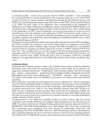
in the connection between the ideality factor and saturation current density shown in Fig. 9
(for different types of solar cells).
1,3 1,4 1,5 1,6 1,7 1,8 1,9 2,0
1E-10
1E-9
1E-8
1E-7
1E-6
7l
10l
5l
4p
1c
1p
J
0
[A/cm
2
]
n
Fig. 9. Saturation current dencity dependence on ideality factor (Vasic et al., 2000).
Direct connection between J
0
and n (nearly exponential increase of saturation current
density with the increase of n) produces the decrease of the efficiency with the increase of
either of these parameters. In the radiation environment, such an increase is usually the
result of induced defects and/or activation of the existent impurities that could act as a
recombination centers for the charge carriers, altering the dominant current transport.
Determination of the dominant current mechanism is very difficult because the relative
magnitude of these components depend on various parameters such as, density of the
interface states, concentration of the impurity defects, and also devises operating voltage.
Existence of the n(V) dependence is the result of such a junction imperfections, leading to
domination of different transport mechanisms in different voltage regions. Therefore,
measuring and monitoring the n(V) dependence which is possible even in working
conditions, could reveal not only the degree of degradation, but also, possible instabilities of
the device in certain voltage regions. This is especially important if those instabilities occur
in the voltage region where maximum power is transferred to the load. Although still in
working condition, performances of such solar cells (efficiency, for most) are considerably
degraded, so that monitoring of the device characteristics should be performed
Solar Cells – Silicon Wafer-Based Technologies
292
continuously, especially if solar cells are exposed to severe working conditions, such as
radiation environment.
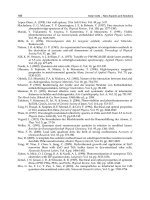
Although effects of gamma irradiation on the solar cells are known to be primarily through
ionization effects, increase of series resistance could also be observed, Fig. 10 (Vasic et al.,
2007, 2010).
0 1000 2000 3000 4000 5000 6000
0
1
2
3
4
5
6
7
8
9
10
R
s
[Ohm]
Dose [kGy]
58
101
255
338
Fig. 10. Dependence of R
s
on doses for polycrystalline solar cells (Vasic et al., 2007).
Almost linear dependence of series resistance on the absorbed irradiation dose indicates
that some changes in the collection of the charge carriers have occurred. This behaviour of R
s
is reflected mostly on the short-circuit current density J
sc
, since radiation induced activation
of defects and impurities mainly affects the transport mechanisms in the device.
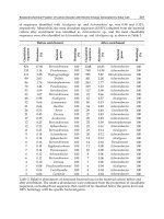
Dependence of the J
sc
on the absorbed dose for different illumination levels was shown in
Fig. 11.
0 1000 2000 3000 4000 5000 6000
0
1
2
3
4
5
6
7
8
9
10
J
sc
[mA/cm
2
]
Dose [kGy]
58
101
255
338
Fig. 11. Dependence of the J
sc
on doses for polycrystalline solar cells (Vasic et al., 2007).
Due to the inevitable presence of surface energy states (as a result of lattice defects,
dislocations, impurities, etc.), after silicon is irradiated with gamma photons, both the
surface recombination velocity and the density of surface states increase. If those states
Characterization of Thin Films for Solar Cells
and Photodetectors and Possibilities for Improvement of Solar Cells Characteristics
293
correspond to deep energy level in the silicon energy gap, they act as efficient surface
recombination centers for charge carriers. Generation of electron-hole pairs due to ionization
effects usually result in the generation and an increase of the noise and minimum signal that
can be detected. All of these effects lead to the decrease of output current. Steeper decrease
of the J
sc
for higher illumination levels indicates that recombination centers could be both
optically activated and activated by irradiation. Therefore, solar cells exposed to the higher
values of solar irradiation during their performance could exhibit greater decrease in the
initial J
sc
.
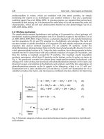
Additionally, if solar cells are polycrystalline, so presence of grain boundaries, characteristic
for the polycrystalline material, has great influence on the collection of the photogenerated
carriers. Presence of the recombination centers, small diffusion length and minority carrier
lifetime, as a result of either irradiation or aging, finally leads to the decrease of the
efficiency of solar cells. As could be seen in Fig. 12, this decrease is very pronounced,
regardless of the illumination level. Although initial efficiencies were slightly different
for different illumination levels, after irradiation they became almost equal, indicating that
radiation gas greater influence on production and transport of charge carriers than
illumination. That, from the standpoint of solar cells, could be very limiting factor for their
performance. Combined influence of the increased 1/f and burst noise due to radiation
induced damage has significant negative influence on major solar cells characteristics.
0 1000 2000 3000 4000 5000 6000
2
3
4
5
6
7
8
9
10
11
12
13
14
15
Efficiency [%]
Dose [kGy]
58
101
255
338
Fig. 12. Dependence of the efficiency on doses (Vasic et al., 2007).
All of this inevitably leads to the decrease of the resolution of the photodetector devices,
lowering solar cells efficiency and for this reason, monitoring of the device characteristics
should be performed continuously, especially when solar cells are exposed to the severe
working conditions.
3.2 Possibilities of the improvement of solar cells and photodetectors
The lifetime decrease of the charge carriers due to the radiation damage induced by
neutrons, produces degradation of electrical parameters of the cell, such as series resistance
(R
s
), output current and finally efficiency (η). High level of series resistance usually indicate
Solar Cells – Silicon Wafer-Based Technologies
294
the presence of impurity atoms and defects localized in the depletion region acting as traps
for recombination or tunneling effects, increasing dark current of the cell (Alexander, 2003,
Holwes-Siedle & Adams, 2002). Moreover, shallow recombination centers in the vicinity of
conducting zone enhance tunneling effect, further degrading output characteristics of the
cell by increasing noise level (especially burst noise that is connected to the presence of
excess current).
Such negative impact of neutron radiation was observed higher illumination level, as could
be seen in Fig. 13 (Vasic et al., 2008). But interesting phenomena – the decrease of series
resistance, was observed for lower values of illumination. (Different behavior for different
illumination level is due to the presence of finite series and parallel resistance in the cell.)
This decrease is very significant from the solar cell design standpoint because it indicates
possible beneficent influence of low doses of irradiation, even with neutrons. It could be
explained by the fact that during fabrication process of any semiconducting device,
structural defects and impurities that were unavoidably made, produce tension in the
crystal lattice. Low doses of radiation could act similarly to annealing, relaxing lattice
structure and decreasing series resistance. Subsequently, this leads to lowering of noise level
and an increase of the output current as shown in Fig.14 (J
m
– current in the maximum
power point).
0 50 100 150 200
3.0
3.5
4.0
4.5
5.0
5.5
6.0
6.5
7.0
7.5
8.0
8.5
9.0
R
s
[Ohm]
Dose [mGy]
32 W/m
2
58 W/m
2
Fig. 13. Dependence of R
s
on doses for two illumination levels (Vasic et al., 2008).
Other parameters of solar cells (voltage in the maximum power point V
m
, fill factor ff and
efficiency) have shown the similar tendencies, which is not surprising since, as it is well
known, high series resistance of the solar cell is one of the main limiting factors of the
efficiency. So, it could be expected that all the main output parameters of the solar cell
should exhibit the same behavior as series resistance in the relation to the irradiation dose.
Finally, improvement of output characteristics after the first irradiation step for low
illumination level is registered for the efficiency also, Fig. 15. Although higher doses of
neutron radiation undoubtedly have negative impact on the performance of solar cells,
observed phenomena give possibilities for using radiation as a method for the improvement
of solar cell characteristics.
Characterization of Thin Films for Solar Cells
and Photodetectors and Possibilities for Improvement of Solar Cells Characteristics
295
0 50 100 150 200
0.6
0.7
0.8
0.9
1.0
1.1
1.2
1.3
1.4
1.5
J
m
[mA/cm
2
]
Dose [mGy]
32 W/m
2
58 W/m
2
Fig. 14. Dependence of the J
m
on doses (Vasic et al., 2008).
0 50 100 150 200
6.0
6.5
7.0
7.5
8.0
8.5
9.0
9.5
10.0
10.5
Efficiency [%]
Dose [mGy]
32 W/m
2
58 W/m
2
Fig. 15. Dependence of the efficiency on doses (Vasic et al., 2008).
Though commonly referred to as a source of noise in semiconducting devices, radiation
induced effects (interaction of neutrons with Si solar cells, in particular) could have in some
cases positive effect on main electrical characteristics (R
s
, J
m
, η). Initial improvement of the
characteristics observed for small doses of neutron radiation and low illumination level,
indicates that there is a possibility of using irradiation for enhancement of the solar cells
quality.
Solar Cells – Silicon Wafer-Based Technologies
296
4. Conclusion
Single element optical detectors such as solar cells and photodiodes are the final component
needed for a communications or optical information processing systems. Due to wide area
of application, they are often exposed to the variety of radiation effects (natural space
environment, atmospheric environment, military and civil nuclear environment). Therefore,
the extensive studies concerning the development of semiconductor devices that can operate
normally in a radiation environment have been undertaken. Although proven to be reliable
in terrestrial applications, solar systems are (like other semiconductor devices) sensitive to
variety of radiation environments in which they are used. Performance failure could have
negative impact both on the financial and environmental aspects of the device application.
From a technological point of view, it is important to study the variations induced by
irradiation of semiconductor junction characteristic parameters (reverse saturation current,
ideality factor etc.), that affect the performance of the solar cells and photodiodes.
5. Acknowledgment
The Ministry of Science and Technological Development of the Republic of Serbia supported
this work under contract 171007.
6. References
Alexander, D.R. (2003). Transient Ionizing Radiation Effects in Devices and Circuits,
IEEE Transaction on Nuclear Sciences, Vol.50, No. 3, pp. 565-582, (2003), ISSN 0018-
9499
Alurralde, M., Tamasi, M. J. L., Bruno, C. J., Martinez Bogado, M. G., Pla, J., Fernandez
Vasquez, J., Duran, J., Shuff, J., Burlon, A. A., Stoliar, P., & Kreiner, A. J. (2004).
Experimental and theoretical radiation damage studies on crystalline silicon
solar cells, Solar Energy Materials & Solar Cells, Vol. 82, pp.531-542, (2004), ISSN
0927-0248
Holwes-Siedle, A.G., & Adams, L. (2002). Handbook of Radiation (Second Edition), Oxford
University Press, ISBN13 9780198507338, Oxford
Horiushi, N., Nozaki, T., & Chiba, A. (2000). Improvement in electrical performance of
radiation-damaged silicon solar cells by annealing, Nuclear Instruments and Methods
A, Vol. 443, pp. 186-193, (2000), ISSN 0168-9002
Hu, Z., He, S., & Yang, D. (2004). Effects of <200 keV proton radiation on electric properties
of silicon solar cells at 77 K, NIM B Beam Interaction with Materials & Atoms, Vol. 217,
pp. 321-326, (2004), ISSN 0168-583X
Jayaweera, P.V.V. , Pitigala, P.K.D.D.P., Perera, A.G.U., & Tennakone, K. (2005). 1/f noise
and dye-sensitized solar cells, Semiconductor Science Technology, Vol. 20, pp.L40-L42,
(2005), ISSN 0268-1242
Jayaweera, P.V.V. , Pitigala, P.K.D.D.P., Senevirante, M.K.I., Perera, A.G.U, & Tennakone, K.
(2007). 1/f noise in dye-sensitized solar cells and NIR photon detectors, Infrared
Physics & Technology, Vol. 50, pp. 270-273, (2007), ISSN 1350-4495
Khan, A., Yamaguchi, M., Ohshita, Y., Dharmaraso, N., Araki, K., Khanh, V.T., Itoh, H.,
Ohshima, T. , Imaizumi, M., & Matsuda, S. (2003). Strategies for improving
Characterization of Thin Films for Solar Cells
and Photodetectors and Possibilities for Improvement of Solar Cells Characteristics
297
radiation tolerance of Si space solar cells, Solar Energy Materials & Solar Cells, Vol.75,
pp. 271-276, (2003), ISSN 0927-0248
Kovačević-Markov, K., Vasić, A., Stanković, K., Vujisić, M. & Osmokrović, P. (2011). Novel
trends in improvement of solar cell characteristics, Radiation Effects and Defects in
Solids, Vol. 166, No. 1, pp. 8-14, (2011), ISSN 1042-0150
Lončar, B., Stanković, S., Vasić, A., & Osmokrović, P. (2005). The influence of gamma and X-
radiation on pre-breakdown currents and resistance of commercial gas filled surge
arresters, Nuclear Technology & Radiation Protection, Vol. XX, No. 1, pp. 59-63, (2005),
ISSN 1451-3994
Lončar, B., Osmokrović, P., Vasić, A., & Stanković, S. (2006). Influence of gamma and X
radiation on gas-filled surge arrester characteristics, IEEE Transactions on Plasma
Science, Vol. 34, No. 4, pp. 1561-1565, (2006), ISSN 0093-3813
Lončar, B., Osmokrović, P., Vujisić, M., & Vasić, A. (2007). Temperature and radiation
hardness of polycarbonate capacitors, Journal of Optoelectronics and Advanced
Materials, Vol. 9, No. 9, pp. 2863-2867, (2007), ISSN 1070-9789
Stojanović, M., Vasić, A., & Jeynes, C. (1996a). Ion implanted silicides studies by frequency
noise level measurements, Nuclear Instruments and Methods B, Vol. 112, pp. 192-195,
(1996),ISSN 0168-583X
Stojanović, M., Jeynes, C., Bibić, N., Milosavljević, M., Vasić, A., & Milošević, Z. (1996b).
Frequency noise level of As ion implanted TiN-Ti-Si structures, Nuclear Instruments
and Methods B, Vol. 115, pp. 554-556, (1996), ISSN 0168-583X
Stojanović, M., Stanković, S., Vukić, D., Osmokrović, P., Vasić, P., & Vasić, A. (1998). PV
solar systems and development of semiconductor materials, Materials Science
Fo
rum, Vols. 282-283, pp. 157-164, (1998), ISSN 0255-5476
Vasić, A., Stojanović, M., Osmokrović, P., & Stojanović, N. (2000). The influence of ideality
factor on fill factor and efficiency of solar cells, Materials Science Forum, Vol. 352, pp.
241-246, (2000), ISSN 0255-5476
Vasić, A., Stanković, S., & Lončar, B. (2003). Influence of the radiation effects on electrical
characteristics of photodetectors, Materials Science Forum, Vol. 413, pp. 171-174,
(2004), ISSN 0255-5476
Vasić, A., Osmokrović, P., Stanković, S. & Lončar, B. (2004). Study of increased temperature
influence on the degradation of photodetectors through ideality factor, Materials
Science Forum, Vol. 453-454, pp. 37-42, (2004), ISSN 0255-5476
Vasić, A., Osmokrović, P., Lončar, B., & Stanković, S. (2005). Extraction of parameters from I-
V data for nonideal photodetectors: a comparative study, Materials Science Forum,
Vol. 494, pp. 83-88, (2005), ISSN 0255-5476
Vasić, A., Vujisić, M., Lončar, B., & Osmokrović, P. (2007). Aging of solar cells under
working conditions, Journal of Optoelectronics and Advanced Materials, Vol. 9 , No. 6,
pp. 1843-1846, (2007), ISSN 1070-9789
Vasić, A., Osmokrović, P., Vujisić, M., Dolićanin, C., & Stanković, K. (2008). Possibilities of
improvement of silicon solar cell characteristics by lowering noise, Journal of
Optoelectronics and advanced Materials, Vol. 10, No 10, pp. 2800-2804, (2008), ISSN
1070-9789
Solar Cells – Silicon Wafer-Based Technologies
298
Vasic,A., Loncar, B., Vujisic, M., Stankovic, K., & Osmokrovic, P. (2010). Aging of the
Photovoltaic Solar Cells, Proceedings of 27th IEEE International Conference on
Microelectronics, pp. 487-490, ISBN 1-4244-0116-x, Nis, Serbia, May 2010
14
Solar Cells on the
Base of Semiconductor-
Insulator-Semiconductor Structures
Alexei Simaschevici, Dormidont Serban and Leonid Bruc
Institute of Applied Physics, Academy of Sciences,
Moldova
1. Introduction
The conventional energy production is not based on sustainable methods, hence exhausting
the existing natural resources of oil, gas, coal, nuclear fuel. The conventional energy systems
also cause the majority of environmental problems. Only renewable energy systems can
meet, in a sustainable way, the growing energy demands without detriment to the
environment.
The photovoltaic conversion of solar energy, which is a direct conversion of radiation
energy into electricity, is one of the main ways to solve the above-mentioned problem. The
first PV cells were fabricated in 1954 at Bell Telephone Laboratories (Chapin et al., 1954); the
first applications for space exploration were made in the USA and the former USSR in 1956.
The first commercial applications for terrestrial use of PV cells were ten years later. The oil
crisis of 1972 stimulated the research programs on PV all over the word and in 1975 the
terrestrial market exceeds the spatial one 10 times. Besides classical solar cells (SC) based on
p-n junctions new types of SC were elaborated and investigated: photoelectrochemical cells,
SC based on Schottky diodes or MIS structures and semiconductor-insulator-semiconductor
(SIS) structures, SC for concentrated radiation, bifacial SC. Currently, researchers are
focusing their attention on lowering the cost of electrical energy produced by PV modules.
In this regard, SC on the base of SIS structures are very promising, and recently the SIS
structures have been recommended as low cost photovoltaic solar energy converters. For
their fabrication, it is not necessary to obtain a p-n junction because the separation of the
charge carriers generated by solar radiation is realized by an electric field at the insulator-
semiconductor interface. Such SIS structures are obtained by the deposition of thin films of
transparent conductor oxides (TCO) on the oxidized silicon surface. A overview on this
subject was presented in (Malik et al., 2009).
Basic investigations of the ITO/Si SIS structures have been carried out and published in the
USA (DuBow et al., 1976; Mizrah et al., 1976; Shewchun et al., 1978; Shewchun et al, 1979)
Theoretical and experimental aspects of the processes that take place in these structures are
examined in those papers. Later on the investigations of SC based on SIS structures using, as
an absorber component, Si, InP and other semiconductor materials have been continued in
Japan (Nagatomo et al., 1982; Kobayashi, et al., 1991), India (Vasu & Subrahmanyam, 1992;
Vasu et al., 1993), France (Manifacier & Szepessy, 1977; Caldererer et al., 1979), Ukraine
Solar Cells – Silicon Wafer-Based Technologies
300
(Malik et al., 1979; Malik et al., 1980), Russia (Untila et al., 1998), the USA (Shewchun et al.,
1980; Gessert et al., 1990; Gessert et al., 1991), Brasil (Marques & Chambouleyron, 1986) and
the Republic of Moldova (Adeeb et al., 1987; Botnariuc et al., 1990; Gagara et al., 1996;
Simashkevich et al., 1999). The results of SIS structures fabrication by different methods,
especially by pyrolitic pulverization and radiofrequency sputtering, are discussed in those
papers. The investigation of electrical and photoelectrical properties of the Si based SIS
structures shows that their efficiency is of the order of 10% for laboratory-produced samples
with an active area that does not exceed a few square centimeters. The spray deposition
method of ITO layer onto the silicon crystal surface results in an efficient junction only in the
case of n-type Si crystals, whereas in the case of p-type silicon crystals radiofrequency
sputtering must be used to obtain good results.
Bifacial solar cells (BSC) are promising devices because they are able to convert solar energy
coming from both sides of the cell, thus increasing its efficiency. Different constructions of
BSC have been proposed and investigated. In the framework of the classification suggested
in (Cuevas, 2005) the BSC structures could be divided into groups according to the number
of junctions: a) two p-n junctions, b) one p-n junction and one high-low junction, and c) just
one p-n junction. In all those types of BSC are based on a heteropolar p-n junction. In this
case, it is necessary to obtain two junctions: a heteropolar p-n junction at the frontal side of
the silicon wafer and a homopolar n/n
+
or p/p
+
junction at its rear side. Usually these
junctions are fabricated by impurity diffusion in the silicon wafer. The diffusion takes place
at temperatures higher than 800
0
C and requires special conditions and strict control. In the
case of the back surface field (BSF) fabrication, these difficulties increase since it is necessary
to carry out the simultaneous diffusion of impurities that have an opposite influence on the
silicon properties. Therefore the problem arises concerning the protection of silicon surface
from undesirable impurities.
The main purpose of this overview is to demonstrate the possibility to manufacture, on the
base of nSi, monofacial as well as a novel type of bifacial solar cells with efficiencies over
10%, containing only homopolar junctions with an enlarged active area, using spray
pyrolysis technique, the simplest method of obtaining SIS structures with a shallow
junction. The utilization of such structures removes a considerable part of the above-
mentioned problems in BSC fabrication. The results of the investigations of ITO/pInP SC
obtained by spray pyrolysis are also discussed.
2. The history of semiconductor-insulator-semiconductor solar cells
First, it must be noted that SC obtained on the base of MIS and SIS structures are practically
the same type of SC, even though they are sometimes considered as being different devices.
The similarity of these structures was demonstrated experimentally and theoretically for
two of the most common systems, Al/SiO
x
/pSi and ITO/SiO
x
/pSi (Schewchun et al, 1980).
The tunnel current through the insulator layer at the interface is the transport mechanism
between the metal or oxide semiconductor and the radiation-absorbing semiconductor,
silicon in this case.
One of the main advantages of SIS based SC is the elimination of high temperature diffusion
process from the technological chain, the maximum temperature at the SIS structure
fabrication not being higher than 450
o
C. The films can be deposited by a variety of
techniques among which the spray deposition method is particularly attractive since it is
simple, relatively fast, and vacuumless (Chopra et al., 1983). Besides, the superficial layer of
Solar Cells on the Base of Semiconductor-Insulator-Semiconductor Structures
301
the silicon wafer where the electrical field is localized is not affected by the impurity
diffusion. The TCO films with the band gap of the order of 3.3-3.7eV are transparent in the
whole region of solar spectrum, especially in the blue and ultraviolet regions, which
increase the photoresponce comparative to the traditional SC. The TCO layer assists with the
collection of separated charge carriers and at the same time is an antireflection coating. In SC
fabrication the most utilized TCO materials are tin oxide, indium oxide and their mixture
known as indium tin oxide (ITO). Thin ITO layers have been deposited onto different
semiconductors to obtain SIS structures: Si (Malik et al., 1979), InP (Botnariuc et al., 1990),
CdTe (Adeeb et al., 1987), GaAs (Simashkevich et al., 1992). Therefore, solar cells fabricated
on the base of SIS structures have been recommended as low cost photovoltaic solar energy
converters. The reduction in cost of such solar cells is due to the simple technology used for
the junction fabrication. The separation of light generated carriers is achieved by a space
charge region that in the basic semiconductor is near the insulator layer.
The number of publications concerning the fabrication and investigation of SIS structures is
very big, therefore we will limited our consideration of the given structures only to those on
the base of the most widespread solar materials – silicon and indium phosphide. To be
exact, main attention will be focused on SC on the base of ITO/nSi and ITO/pInP.
2.1 SIS structures on the base of silicon crystals
As shown above, one of the ways to solve the problem of the cost reduction of the electrical
energy provided by SC is to use SIS structures. First publications regarding the obtaining
and investigation of ITO/nSi structures appeared in 1976. (Mizrah & Adler, 1976). Power
conversion efficiencies of 1% were reported for an ITO/nSi cell, obtained by the magnetron
dispersion of ITO layers on the surface of nSi crystals with an active area of 0.13 cm
2
. The
data obtained from the investigated I-V dark characteristics and known band gaps and the
work functions of ITO and Si allows to make the band diagram of these structures (Fig. 1).
The efficiency of 10% was observed for ITO/nSi cells, obtained by the spray deposition of
ITO layers onto nSi crystals with the area of 0.1 cm
2
(Manifacier & Szepessy 1977; Calderer
et al., 1979). ITO/nSi SC with the power conversion efficiencies of 10% were fabricated by
deposition onto n-type Si crystals by the electron- beam evaporation of a mixture of 90:10
molar % In
2
O
3
: SnO
2
powder (Feng et al., 1979).
The results of those works have been analyzed in detail (Shewchun et al., 1978; Shewchun et
al., 1979) from both experimental and theoretical points of view. Given the general theory of
heterojunctions is incomprehensible, how they can work as effective SC formed by materials
with different crystalline types and lattice constants, when an intermediate layer with many
defects appears at the interface. It is intriguing to note here that various authors have
received quite contradictory results. Examining these data, authors in (Shewchun et al.,
1979) concluded that the performance of those SC depended on the intermediate thin
insulator layer. Its main function is the compensation of the defects due to the mismatches
of the crystalline lattices. Its thickness is not greater than 30Å, which ensures the tunnel
transport of the carriers through the barrier. The theoretical analysis of ITO/nSi solar cell
has shown that they are similar to MIS structures: their parameters depend on the thickness
of the insulating layer at the interface, the substrate doping level, concentration of surface
states, oxide electric charge and temperature. The optimization of these parameters can
provide 20% efficiency.
In (Shewchun et al., 1979) this issue was examined in terms of energy losses during
conversion of sunlight into electricity. Different mechanisms of energy loss that limit
Solar Cells – Silicon Wafer-Based Technologies
302
ITO/nSi solar cell efficiency are probably valid for other SIS structures too. Dark current-
voltage characteristics were used as experimental material and it was shown that after a
certain threshold of direct voltage these characteristics do not differ from similar
characteristics of p-n junctions in silicon, and the current is controlled by diffusion processes
in silicon volume. Different mechanisms of energy loss that limit ITO/nSi solar cell
efficiency are presented in Table 1 (Shewchun et al., 1979).
Fig. 1. Energy band diagram of the ITO/nSi/n
+
Si structure (a) - in the dark, (b) - at solar
illumination under open circuit conditions. The shaded area - the insulating SiOx layer.
Solar Cells on the Base of Semiconductor-Insulator-Semiconductor Structures
303
Mechanism Loss rate
1. Absorption and reflection in the ITO layer up to 8%
2. Recombination in space charge region 0.1 1%
3. V
CD
height reduction 0 – 12%
too high work function 0-3%
inhomogeneous SiO
x
layer 0-3%
low doped ITO layer 0-3%
too large saturation current 0-3%
4. Low fill factor 0-10%
series resistance of the intermediate layer
series resistance of the contacts
shunt
Table 1. The energy loss mechanisms, which do not provide the maximum possible
efficiency of 20%
An increase of the conversion efficiency of SC based on ITO/nSi structures can be achieved
by the optimization of the thickness of the frontal ITO layer and of the insulator SiO
2
layer;
the optimization of the concentration of electrons in absorbing Si wafers; the texturing of the
Si wafers surface.
The thickness of the frontal ITO layer is a very important factor because it affects the
quantity of the absorbed solar radiation depending on both absorption and reflection. It is
necessary to select such ITO layer thickness that determines a large minimum of the
reflection in the region of maximum sensitivity of the n
+
ITO/SiO
2
/nSi SC. At the same time,
the thickness of the frontal ITO layer determines their electrical resistance and, therefore, the
value of the photocurrent, but for all that, the growing of the ITO layer thickness has an
contrary effect on the solar cells efficiency, diminishing the absorption and increasing the
photocurrent. At the same time, the thickness of the frontal ITO layer determines the
efficiency of this layer as an anti reflection coating.
The properties of the SIS structures, largely, also depend on the thickness of the SiO
2
insulator layer at ITO/Si interface. This SiO
2
layer increases the height of the junction
potential barrier and diminishes the saturation current. Besides, the insulator SiO
2
layer
must be tunnel transparent for charge carrier transport. The optimal SiO
2
insulator layer
thickness must be not more than some tens of Å.
All silicon wafers must be oriented in the (100) plane because only such crystallographic
orientation could be used to get a potential barrier by ITO spray deposition. Single
crystalline Si wafers with different carrier concentration from 10
15
cm
-3
up to 10
18
cm
-3
have
been used to fabricate ITO/nSi SIS structures by spray deposition.
The influence of the structural state of the Si single crystalline wafers on the conversion
efficiency will be discussed in the next section of this overview.
The paper (Feng et al., 1979) studied the current transport mechanism of ITO/Si structures,
the TCO layer beings obtained by evaporation under the action of an electron beam. Pre-
treatment of Si crystals with Cl
2
has led to the increased yield from 2.3% to 5.5%. In this case
the current transport mechanism was dominated by recombination in the space charge
Solar Cells – Silicon Wafer-Based Technologies
304
layer, while there is the thermo emission over the potential barrier in the absence of Cl
2
.
Systematical studies of the properties of the ITO/nSi structures, obtained by spray
pyrolysis, were carried out in 1980 (Ashok et al., 1980). The optical and electrical
characteristics of the IT0 layer as well as the thickness of the insulator layer have been
optimized to yield the following photovoltaic parameters on 0.5Ohm·cm nSi: V
oc
= 0.52V,
J
sc
=31.5mA/cm
2
, FF=0.70, conversion efficiency is 11.5%. The dark I-V and C-V
characteristics have also been evaluated to identify the mechanisms of barrier formation and
current flow. C-V data indicate an abrupt heterojuncton, while dark I-V characteristics are
suggestive of a tunneling process to determine current flow in these devices in conformity
with the Riben and Feucht model (Riben & Feucht, 1966). A comparison of spray deposited
ITO/nSi and SnO
2
/nSi was presented by Japanese researchers (Nagatomo et al. 1982). The
diode and photovoltaic properties of these structures are very similar, but the conversion
efficiency of ITO/nSi is higher, up to 11-13%, whereas for SnO
2
/nSi these values do not
exceed 7.2% (Nagatomo et al., 1979). As is reported in the paper (Malik et al., 2008; Malik et
al., 2009), the authors fabricated ITO/nSi solar cells using n-type single crystalline silicon
wafers with a 10Ohm·cm resistivity and an 80nm thick ITO film with a sheet resistance of
30Ohm/□ that was deposited by spray pyrolysis on the silicon substrate treated in the H
2
O
2
solution. This ITO thickness was chosen in order to obtain an effective antireflection action
of the film. The cells obtained in such a way can be considered as structures presenting an
inverted p-n junction (Fig. 2).
Fig. 2. Energy diagram (in kT units) of the heavy doped ITO/n-Si heterojunction
Under the AM0 and AM1.5 solar illumination conditions, the efficiency is 10.8% and 12.2%,
respectively. The theoretical modeling based on p-n solar cells shows an excellent agreement
between the theoretical and the experimental results. It is also shown that using 1Ω·cm
silicon substrates is a promising alternative for obtaining solar cells with 14% efficiency
under AM1.5 illumination conditions.
Various models for energetic band diagrams and the carrier transport mechanism in SIS
ITO/nSi cells have been proposed so far. Among them are the thermo ionic emission as the
dominant charge transport mechanism in the SC obtained by spray deposition of SnO
2
onto
nSi crystals (Kato et al., 1975), and the recombination current in the depletion layer for the
CVD deposited ITO/nSi junction (Varma et al., 1984). Majority of authors suggested that
Solar Cells on the Base of Semiconductor-Insulator-Semiconductor Structures
305
trap –assisted multi step tunneling through the depletion layer is the determinant current
flow mechanism (Ashok et al., 1980; Saim & Campbell, 1987; Kobayashi et al., 1990;
Simashkevich et al., 2009).
The mechanism of the current transport through the potential barrier is determined by the
energetic band diagram and the height of the barrier. When the later is very high, a physical
p-n junction is formed in Si crystals near the surface (Fig. 2). Otherwise, the ITO/nSi SC
operate as MIS structures or Schottky diodes (Fig. 1). Some data about the efficiencies of
ITO/nSi SC are presented in Table 2.
References ITO deposition method Area (cm
2
) Eff. (%) Note
Mizrah et al., 1976 R.F. Sputtering 0.13 1
Manifacier et al., 1977 Spray 1.5 10
Feng et al., 1979 Electron beam 1 - 4 10
Calderer et al., 1979 Spray 1.5 10
Ashok et al., 1980 Spray 0.3 11.5 BSF
Nagatomo et al., 1982 Spray 11-13
Gagara et al., 1996 Spray 10.1
Vasu et al., 2005 Electron beam 1.0 5.5
Malik et al., 2008 Spray 1 - 4 11.2
Table 2. Efficiencies of ITO/nSI solar cells fabricated by various deposition techniques of
ITO films on smooth (non textured) Si crystal surfaces
The analysis of the works referred to shows that the conversion efficiency of ITO/nSi solar
cells obtained by various methods is about 10% and in some cases reaches 12%. Their active
area is not more than a few square centimeters, which is not enough for practical
application.
2.2 ITO/nSi solar cells with textured surface of Si crystalls
As can be seen from Table 1, the optical losses of ITO/nSI solar cells are up to 8%, other
estimates show that they can exceed 10% (Garcia et al., 1982). Those losses depend on the
surface state of silicon wafers and can be minimized by creating a textured surface of the
light absorbing semiconductor material, thus reducing the reflection and increasing the
absorption. The texturization leads to the enlargement of the junction area of a photovoltaic
cell and to the increase of the conversion efficiency. The enlargement of the junction area in
the case of silicon crystals is usually achieved by means of selective chemical etching in
KOH (Bobeico et al., 2001; Dikusar et al., 2008; Simashkevich et al., 2011). As a result,
pyramids or truncated cones with the base dimensions of 5μmx5μm or with a diameter of
10μm on the Si surface are formed.
The efficiency of 12.6% under AM1 simulated irradiation was obtained for SnO
2
: P/SiO
2
/nSi
SC with the active area of 2cm
2
(Wishwakarma et al., 1993) Those cells were fabricated by
deposition of SnO
2
layers doped with P by CVD method on the textured surface of the Si
crystals with resistivity of 0.1 Ohm.cm. SiO
2
insulating layer was obtained by chemical
Solar Cells – Silicon Wafer-Based Technologies
306
methods. The textured surface of the Si crystals reduces the frontal reflectivity, and
consequently increases the short circuit current by around 10%.
ITO/nSI obtained by spray deposition of ITO layers on nSi wafers oriented in (100) plane,
were obtained in Japan (Kobayashi et al, 1990). The final size of the active area of the cell
was 0.9cm x 0.9cm. Mat-textured Si surfaces were produced by the immersion of the Si
wafers in NaOH solution at 85
0
C. For so treated specimens the solar energy conversion
efficiency of 13% was attained under AM1 illumination.
The paper (Simashkevich et al., 2011) studied the properties of ITO/nSi SC with improved
parameters. The performed optimization consists in the following: the optimization of the
thickness of the frontal ITO layer and of the thickness of the insulator SiO
2
layer; the
optimization of the concentration of the electrons in absorbing Si wafers; the texturing of the
Si wafers surface.
The performed investigations make it possible to come to the following conclusions. The
optimum thickness of the frontal ITO layer was determined experimentally from the
photoelectric investigations and is equal to 0.5μm. The SiO
2
layer can be obtained by
different methods. In the case of fabrication n
+
ITO/SiO
2
/nSi solar cells by spray pyrolysis,
the optimal SiO
2
layer thickness was obtained by a combined thermo chemical method
selecting the temperature regime and the speed of the gas flow during ITO layer deposition.
The optimal SiO
2
insulator layer thickness, measured by means of ellipsometric method, is
about 30-40Å.
To determine the optimal electron concentration ITO/nSi SIS structures were investigated
obtained by ITO spray deposition on the surface of phosphor and antimony doped single
crystalline Si wafers with different carrier concentrations: 10
15
cm
-3
, 5·10
15
cm
-3
, 6·10
16
cm
-3
, and
2·10
18
cm
-3
, produced in Russia (STB Telecom) and Germany (Siltronix, Semirep). The
investigation of the electrical properties of n
+
ITO/SiO
2
/nSi SC shows that the optimum
values of the barrier height, equal to 0.53eV and the space charge region thickness equal to
W=0.36μm, have been obtained in the case of Si crystals with the electron concentration
5·10
15
cm
-3
. Carrier diffusion length (L) is one of the main parameters for bifacial solar cells.
For this silicon crystal L is about 200μm. The BSF region at the rear side of the cell was
obtained by phosphor diffusion.
To enlarge the active area and reduce optical losses due to radiation reflection, the active
area of Si wafer, oriented in a plane (100), was exposed to the anisotropic etching.
The etching was spent by two expedients for reception of the irregular and regular
landform. In both cases, the boiling 50% aqueous solution of KOH was used as the etching
agent. The processing time was 60 - 80s. In the first case, the etching process was yielded
without initially making a landform on the silicon wafer surface for the subsequent
orientation of the etching process.
Fig. 3a shows that the landform of the silicon surface is irregular and unequal in depth. The
depth of poles of etching is within the limits of 2-3μm.
In the second case, the method of making the ranked landform in the form of an inverse
pyramid was applied. The chemical micro structurisation of the silicon wafer surface was
carried out in the following order: the deposition of a SiO
2
thin film with 0.1μm thickness by
electron beam method; the deposition on the SiO
2
thin film of a photo resists layer and its
exposure to an ultraviolet radiation through a special mask; removal of the irradiated photo
resist and etching SiO
2
with HF through the formed windows; removal of the remaining
photo resist thin film. The anisotropic etching of the silicon surface through the windows in
SiO
2
thin film was carried out. The result of this type of etching is shown in Fig. 3b.
Solar Cells on the Base of Semiconductor-Insulator-Semiconductor Structures
307
(a)
(b)
Fig. 3. Images of the silicon wafers surface landform a) irregular etching; b) regular etching
It is evident that the micro structured surface represents a plane with a hexagonal ornament
formed by inverse quadrangular pyramids with 4μm base and 2-3μm depth.
After the deposition of ITO layers on the both types of the textured surfaces of the silicon
wafers (Fig. 3) and Cu evaporated grid on the frontal side and continuous Cu layer on the
rear side, two types of the optimized structures have been fabricated (Fig. 4).
Fig. 4. The schematic image of ITO/SiO
2
/nSi/n
+
Si solar cell with optimized parameters and
textured Si surface
Solar Cells – Silicon Wafer-Based Technologies
308
The measurements of these characteristics and of solar energy conversion efficiency have
been carried out under standard conditions (AM1.5, 1000W/m
2
, 25
0
C) with the solar
simulator ST 1000. The load I-V characteristics of the n
+
ITO/SiO
2
/n/n
+
Si SC are presented
in Fig. 5 and Fig. 6.
0.00.10.20.30.40.5
0
5
10
15
20
25
30
35
Standart condition
1000W/m
2
, 25
o
C, AM1.5
J
sc
= 34.0mA/cm
2
U
oc
= 0.504V
FF = 69.3%
Eff.= 11.88%
R
ser
= 3.586 Ohm
R
sh
= 9131 Ohm
Current density,mA/cm
2
Voltage,V
Fig. 5. Load I-V characteristic of ITO/SiO
2
/nSi solar cells with irregular landform Si surface
0.0 0.1 0.2 0.3 0.4 0.5
0
10
20
30
40
Current density,mA/cm
2
Voltage,V
Standart condition
1000W/m
2
, 25
o
C, AM1.5
J
sc
= 40.6mA/cm
2
U
oc
= 0.507V
FF = 76.5%
Eff.= 15.79%
R
ser
= 3.860 Ohm
R
sh
= 1389 Ohm
Fig. 6. Load I-V characteristic of ITO/SiO
2
/nSi solar cells with regular landform Si surface
For samples obtained on textured Si wafers with irregular landform (Fig. 5), the efficiency
and other photoelectric parameters increased in comparison with the SC described earlier
(Gagara et al, 1996, Simashkevich et al, 1999). Besides, the results improved when Si wafers
Solar Cells on the Base of Semiconductor-Insulator-Semiconductor Structures
309
with regular landform (Fig.3b) were used for ITO/SiO
2
/nSi solar cell fabrication. The
respective load I-V characteristic is presented in Fig. 6.
The summary data regarding the methods of ITO layer deposition onto the textured silicon
wafers and the obtained efficiencies are presented in Table 3.
References
ITO deposition
method
Area
(cm
2
)
Eff.
(%)
Note
Kobayashi et al., 1991 Spray 2.25 13 Textured Si surface
Vishvakarma et al.,
1993
CVD 2.0 12.6 Textured Si surface
Simashkevich et al.,
2011
Spray 4.0 11.88
Irregular texture Si
surface
Simashkevich et al.,
2011
Spray 4.0 15.79 Regular texture Si surface
Table 3. Efficiencies of ITO/SiO
2
/nSi solar cells fabricated by various deposition techniques
of ITO layers onto the textured silicon wafers
2.3 SIS structures on the base of InP and other crystals
Indium phosphide is known to be one of the most preferable materials for the fabrication of
solar cells due to its optimum band gap; therefore, it is possible to obtain solar energy
conversion into electric power with high efficiency. On the base of InP, SC have been
fabricated with the efficiency of more than 20 % (Gessert, et al, 1990). In addition, InP based
SC are stable under harsh radiation conditions. It was shown (Botnaryuk, Gorchiak et al.,
1990, Yamamoto et al, 1984, Horvath et al, 1998) that the efficiency of these SC after proton
and electron irradiation decreases less than in the case of Si or GaAs based SC. However,
due to the high price of InP wafers, in terrestrial applications, indium phosphide based SC
could not be competitive with SC fabricated on other existing semiconductor solar materials
such as silicon.
2.3.1 Fabrication of ITO/InP photovoltaic devices
Let us consider the fabrication process of ITO/InP photovoltaic devices. Two main methods
of the ITO layer deposition onto InP crystals are used. The first method consists in the
utilization of an ion beam sputtering system (Aharoni et al., 1986). The fabrication process of
InP photovoltaic devices using this method and the obtained results are described in detail
elsewhere (Gessert et al., 1990; Aharoni et al., 1999).
A schematic diagram of the ITO/InP solar cell fabricated by the above-mentioned method is
presented in Fig. 7. The operation of solar cells shown in Fig. 7 can be attributed to two
possible mechanisms. One is that the conductive ITO and the substrate form an nITO/pInP
Schottky type barrier junction. The second is the formation of a homojunction due to the
formation of a “dead” layer (thickness – d) at the top of the InP substrate. This “dead” layer
is caused by the crystal damage, which results from the impingement of the particles
sputtered from the target on the InP top surface. The “dead” layer volume is characterized
by extremely short free carrier’s life times, i.e. high carrier recombination rates, with respect
to the underlying InP crystal.
Solar Cells – Silicon Wafer-Based Technologies
310
Fig. 7. Schematic diagram of the ITO/InP photovoltaic device obtained by ion bean sputtering.
Accordingly, it forms the “n” side of a homojunction with the “p” type underlying InP. The
formation of an n-p junction in InP may be due to tin diffusion from the ITO into the InP,
where tin acts as a substitution donor on In sites. The record efficiency of 18.9% was
obtained in (Li et al., 1989) for ITO/InP structures, when the ITO layer was deposited by
magnetron dispersion on p
+
p/InP treated preliminary in Ar/O
2
plasma.
Using the above-described sputtering process, a small-scale production of 4cm
2
ITO/InP
photovoltaic solar cells has been organized at Solar Energy Research Institute (now National
Renewable Energy Laboratory), Golden, Colorado, the USA (Gessert et al., 1991). Although
only a small number of the 4cm
2
ITO/InP cells (approximately 10 cells total) were
fabricated, the average cell efficiency is determined to be 15.5%, the highest cell performance
being 16.1% AM0. Dark I-V data analysis indicates that the cells demonstrate near-ideal
characteristics, with a diode ideality factor and reverse saturation current density of 1.02 and
1.1·10
-12
mA/cm
2
, respectively (Gessert et al, 1990).
The second, a simpler, method of ITO/InP photovoltaic devices fabrication consists in
spray-pyrolitic deposition of ITO layers onto InP substrates (Andronic et al., 1998;
Simashkevich et al., 1999; Gagara et al., 1986; Vasu et al, 1993). ITO layers were deposited on
the surface of InP wafers by spraying an alcoholic solution of InCl
3
and SnCl
4
in different
proportions. The following chemical reactions took place on the heated up substrate:
4InCl
3
+ 3O
2
= 2In
2
O
3
+ 6Cl
2
(1)
SnCl
4
+ O
2
= SnO
2
+ 2Cl
2
(2)
ITO thin films with the thickness of 150-250nm were deposited by the above-mentioned
spray method in various gaseous environments: O
2
, Ar, or air atmosphere. When the inert
gas was carrier gas, the installation could be completely isolated from the environment that
allowed obtaining the structures in the atmosphere without oxygen. A thin insulator layer
with the thickness up to 10nm is formed on InP surface due to the oxidation of the substrate
during spraying. The oxidation of InP wafers in HNO
3
for 20-30s was realized in the case of
inert gas atmosphere. In the case of InP crystals, a thin insulator P
2
O
5
layer with the
thickness 3-4 nm was formed on InP wafer surface during the ITO layers deposition. Ohmic
contacts to pInP were obtained by thermal vacuum evaporation of 95 % Ag and 5 % Zn alloy
on the previously polished rear surface of the wafer.
Solar Cells on the Base of Semiconductor-Insulator-Semiconductor Structures
311
Structures with different crystallographic orientation and holes concentration in the InP
substrates were obtained. The optimum concentration of the charge carriers in plnP
substrates was 10
16
cm
-3
, but the InP wafers with these carrier concentrations and the
thickness of 400 nm had a high resistance. For this reason, p/p
+
InP substrates were used in
order to obtain efficient solar cells with a low series resistance. In some cases a plnP layer
with the thickness up to 4 µm and concentration p = (3 30)·10
16
cm
-3
was deposited by the
gas epitaxy method from the InPCl
3
H
2
system on the (100) oriented surface of InP heavily
doped substrate with the concentrations p
+
= (1 3)·10
18
cm
-3
for the fabrication of
ITO/pInP/p
+
InP structures. Ag and 5 % Zn alloy evaporated in a vacuum through a special
mask were used as an ohmic contact to the ITO and to InP crystal. A schematic diagram of
ITO/p/p
+
InP structure obtained by spray pyrolitic method is presented in Fig. 8.
Fig. 8. Schematic diagram of the ITO/InP structure obtained by spray pyrolitic method.
2.3.2 Electrical properties of ITO/InP solar cells
The energy band diagram of the ITO/pInP structure proposed in (Botnariuc et al., 1990) is
presented in Fig. 9. The current flow mechanism of the ITO/InP structures, obtained in
different fabrication conditions, was clarified in (Andronic et al., 1998) on the base of the
energy band diagram below.
Fig. 9. Energy band diagram of ITO/InP structure obtained in oxygen atmosphere
Solar Cells – Silicon Wafer-Based Technologies
312
The I-V characteristics of ITO/pInP structures at different temperatures, obtained in the
non- oxide environment are given in Fig. 10a.
(a) (b)
Fig. 10. Dark current-voltage characteristics at direct bias a) obtained in nitrogen
atmosphere: b) obtained in oxygen atmosphere
One can suppose the existence of two channels of carriers transport through the structure
interface (insertion in Fig. 10a). The first channel is the following: the majority carriers from
InP are tunneling through the barrier at the interface and then recombining step by step
with electrons from ITO conduction band (Riben & Feucht, 1966). According to this model,
the I-V characteristic slope should not depend on temperature. The second channel appears
at the direct bias of more than 0.6V and is determined by the emission of electrons from the
ГГО conduction band to the InP conduction band This emission should occur by changing
the I-V curves slope at different temperatures. As one can see from the experimental data,
these two channels are displayed by two segments on I-V characteristics.
Fig. 10b shows the I-V characteristics of the ITO/InP structures achieved in an oxygen
environment or under substrate oxidation. In this case, the presence of the insulator layer on
the interface could be expected. The ITO/InP structures capacity-voltage measurements
confirm this supposition. During the fabrication of the ITO/InP structure in oxygen
atmosphere, a thin insulator layer on the interface is obtained. Changing the segment II from
the ITO/InP structure I-V characteristics shows the presence of a thin insulator layer. The
insulator presence leads to changing the process of electron emission from the ITO conduction
band to the InP conduction band on the tunneling process through this insulator layer. Thus,
the form of segment II on the I-V characteristics becomes similar to the segment I form.
2.3.3 Photoelectric properties of ITO/InP solar cells
Photoelectric properties of these SC have been investigated at the illumination of the
heterostructures through the wide gap oxide layer. For all investigated samples, the current-
voltage characteristics at illumination do not differ from the characteristics of respective
Solar Cells on the Base of Semiconductor-Insulator-Semiconductor Structures
313
homojunction solar cells. The current short circuit I
sc
linearly depends on the illumination
intensity; the open circuit voltage U
oc
changes with the illumination after the usual
logarithmic dependence:
ln 1
sc
oc
o
I
kT
U
qI
(3)
where I
L
- light induced current, I
s
- the saturation current, T- temperature.
The dependence of ITO/InP cells parameters in AM 0 conditions versus InP substrate
orientation and hole concentration was studied. InP wafers with the orientation in (100) and
(111) B directions were used to obtain solar cells by the deposition of ITO layers (Table 4).
Substrate p, 10
16
cm
-3
V
oc
,
(mV) I
sc
,
(mA/cm
2
) η, (%)
pInP (111)B
2.6
6.5
15
674
699
689
28.3
23.8
25.3
10.4
9.6
9.5
p
+
/pInP (100)
10
30
2.0
707
695
707
25.9
28.6
30.8
11.1
11.0
11.6
pInP (111)A
3.7
5.7
37
568
722
545
22.0
17.7
14.3
5.0
5.3
3.7
Table 4. The dependence of ITO/InP cells parameters in AM0 conditions versus InP
substrate crystallographic orientation
The photo sensibility spectral distribution of the p
+
/pInP(100) structure is presented in Fig. 11.
400 500 600 700 800 900 1000
0.0
0.1
0.2
0.3
0.4
0.5
0.6
I
sc
/E (A/W)
(nm)
Fig. 11. The photo sensibility spectral characteristic of the p
+
/pInP (100) SC
The region of the spectral sensibility of Сu/nITO/pInP/Ag:Zn structure is situated between
400 - 50 nm.
Solar Cells – Silicon Wafer-Based Technologies
314
The minimum efficiency was observed when solar cells were obtained by deposition of ITO
layers onto InP wafers oriented in (111) A direction. To increase the efficiency, those solar
cells were thermally treated in H
2
atmosphere at the temperature of 350
0
C during 10
minutes to reduce the series resistance (Bruk et al, 2007).
It was shown that before the thermal treatment the following parameters had been obtained
under AM 1.5 illumination conditions: U
oc
= 0.651 V, I
sc
= 18.12 mA/cm
2
, FF = 58 %,
Eff. = 6.84 % (Fig. 12, curve 1).
-0.2 0.0 0.2 0.4 0.6 0.8
-0.02
-0.01
0.00
0.01
3
2
1
J (A/cm
2
)
U (V)
Fig. 12. Load I-V characteristics of Сu/nITO/pInP/Ag:Zn solar cells: 1-before thermal
treatment; 2-after thermal treatment in H
2
; 3-best parameters after thermal treatment in H
2
After the thermal treatment the parameters were: U
oc
= 0.658 V, I
sc
= 20.13 mA/cm
2
, FF = 58%,
Eff.= 7.68 % (Fig.12, curve 2). The photoelectric parameters of the SC received on InP wafers
with the concentration p = 3.10
17
cm
-3
after the thermal treatment were U
oc
=0.626 V, I
sc
= 22.72
mA/cm
2
, FF = 71 %, Eff.= 10.1 % (Fig. 12, curve 3), that is better than for analogous SC
without treatment in H
2
.
The thermal treatment in H
2
leads to the undesirable decrease of the photo sensibility in the
short wave region of the spectrum (Fig.13).
The highest sensibility is observed at 870nm, which indicates that the maximum
contribution in the photo sensibility is due to the absorption in InP.
ITO/InP structures grown by spray pyrolysis were also investigated in Semiconductor
Laboratory of the Indian Institute of Technology, Madras (Vasu & Subrahmanyam, 1992;
Vasu, et al., 1993). The maximum efficiency of 10.7% was achieved under 100mW/cm
2
illumination for junctions having 5% by weight of tin in the ITO films. The texturing of
the InP crystal surface in ITO/InP SC (Jenkins et al., 1992) reduces the surface reflection.
These cells showed improvement in both short circuit current and fill factor, the efficiency
can be increased by 6.74%. The texturing reduces the need for an optimum antireflection
coating.
Solar Cells on the Base of Semiconductor-Insulator-Semiconductor Structures
315
SIS structures for SC fabrication were also obtained on the base of other semiconductor
materials besides Si and InP. ITO/CdTe (Adeeb et al., 1987) and ITO/GaAs (Simashkevich
et al., 1992) structures were obtained by spray pyrolysis of ITO layers on pCdTe and pGaAs
crystals. For ITO/CdTe the efficiency was 6%, for ITO/GaAs SC it did not exceed 2.5%.
400 500 600 700 800 900 1000
0
20
40
60
80
100
120
140
160
180
2
1
I
sc
(arb.un.)
(nm)
Fig. 13. The spectral photo sensibility of Cu/n+ITO/pInP/Ag:Zn structure: 1- before H
2
annealing, 2- after H
2
annealing
2.3.4 Degradation of photoelectric parameters of ITO/InP solar cells exposed to
ionizing radiation
The degradation of photoelectric parameters of ITO/InP solar cells after their irradiation by
protons with energies E
p
=20.6MeV and flux density up to F
p
=10
13
cm
-2
and by electrons with
E
c
=1MeV and F
e
≤10
15
cm
-2
was investigated (Andronic et al., 1998). The results of the
photoelectrical parameter measurements at AM0 conditions after the irradiation are
presented in Fig. 14.
Higher efficiency of 11.6% is obtained if the InP substrate is oriented in [100] plane.
Fig. 14. The degradation of ITO/InP heterostructures photoelectric parameters under
protons (a) and (b) electrons irradiation