Optoelectronics Devices and Applications Part 15 doc
Bạn đang xem bản rút gọn của tài liệu. Xem và tải ngay bản đầy đủ của tài liệu tại đây (4.82 MB, 40 trang )
Optoelectronics in Suppression Noise of Light
549
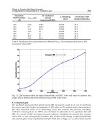
photocurrent fluctuation is shown in Fig. 9, with 200,000 points for each curve. The points in
the figure are the experimental results, and the solid curves are Gaussian fits of the
probability distribution. Curve a represents the probability distribution of the prepared sub-
Poissonian field, curve b corresponds to a coherent state (the SNL), and curve c corresponds
to single-beam field without correction. It is shown that the sub-Poissonian distribution of
light fluctuation is narrower than a standard Gaussian distribution of the coherent state. The
uncorrected single-beam fluctuation distribution is a super-Poissonian and is much broader
than the standard Gaussian distribution. The photocurrent fluctuation of the sub-Poissonian
field can also be compared with the standard Gaussian distribution. A noise reduction of 1.2
dB below the SNL is calculated from average half-widths (Fig. 9) and does not accord well
with what we observed with the spectrum analyzer because of the narrow bandwidth of the
prepared sub-Poissonian field and a nonideal low-pass filter. The calculated photocurrent
fluctuation of a single beam is 9 dB above the SNL, which accords well with what we
observed with the spectrum analyzer.
Fig. 8. (Color online) (a) Normalized sub-Poissonian light noise from 1079 to 1083.7 nm. (b)
Wavelength of twin beams versus temperature of the crystal in the OPO.
Optoelectronics – Devices and Applications
550
Fig. 9. (Color online) Intensity fluctuation distribution at 5.5 MHz. Curve
a, prepared sub-
Poissonian field; curve
b, coherent light; curve c, single beam from the NOPO (beam A).
4. Conclusion
We introduce the application of opto-electronics feed-forward in noise suppression,
including both classical noise (fiber laser noise suppression) and quantum noise (preparing
sub-Poissonian) suppression. The technique of opto-electronics has been widely applied and
will be more and more significant in the field of quantum optics and quantum information.
5. References
Andersen, U.; Josse,V. & Leuchs, G. (2005). Unconditional Quantum Cloning of Coherent
States with Linear Optics. Phys.Rev. Lett. Vol. 94, No. 24, pp.240503, ISSN:1079-
7114.
Ball, G.; Hull-Allen,G. & Holton, C. (2008). Low noise single frequency linear fiber laser.
Electronics Letters. Vol. 29, No. 18, pp. 1623-1625, ISSN: 0013-5194.
Braunstein, S. Nicolas, J.; Iblisdir, S.; Loock, P. & Massar, S. (2001). Optimal Cloning of
Coherent States with a Linear Amplifier and Beam Splitters. Phys.Rev. Lett. Vol. 86,
No. 21, pp.4938-4941, ISSN:1079-7114.
Cheng, Y.; Kringlebotn, J.; Loh, W.; Laming, R. & Payne, D. (1995). Stable single-frequency
travelling-wave fiber loop laser with integral saturable-absorber-based tracking
narrow-band filter. Opt. Lett. Vol. 20, No. 8, pp. 875-877, ISSN:0146-9592.
Dong, R.; Lassen, M.; Heersink, J.; Marquardt, C.; Filip, R.; Leuchs, G. & Andersen, G. (2008).
Experimental entanglement distillation of mesoscopic quantum states. Nature
Phys. Vol. 4, No. 2 November, pp.919-923, ISSN:1745-2473.
Optoelectronics in Suppression Noise of Light
551
Furusawa, A.; Sørensen, J.; Braunstein,S.; Fuchs, C.; Kimble, H. & Polzik, E. (1998).
Unconditional Quantum teleportation. Science. Vol.282, No.5389, pp.706-709,
ISSN:1095-9203.
Hage, B.; Samblowski, A.; DiGuglielmo, J.; Franzen, A.; Fiurášek, J. & Schnabel, R. (2008).
Preparation of distilled and purified continuous-variable entangled states. Nature
Phys. Vol. 4, No. 2 November, pp.915-918, ISSN:1745-2473.
Kim, C. & Kumar, P. 1992. Tunable sub-Poissonian light generation from a parametric
amplifier using an intensity feedforward scheme. Phys.Rev. A. Vol. 45, No. 7,
pp.5237-5242, ISSN:1050-2947.
Lam, P.; Ralph, T.; Huntington, E. & Bachor, H. (1997). Noiseless Signal Amplification using
Positive Electro-Optic Feedforward. Phys.Rev. Lett. Vol. 79, No. 8, pp.1471-1474,
ISSN:1079-7114.
Laurat, J.; Coudreau, T.; Treps, N.; Maitre, A. & Fabre, C. (2003). Conditional Peraration of a
Quantum State in the Continuous Variable Regime: Generation of a sub-Poissonian
State from Twin Beams. Phys.Rev. Lett. Vol. 91, No. 21, pp.213601, ISSN:1079-7114.
Li, R.; Choi, S. & Humar, P. (1995). Generation of sub-Poissonian pulses of light. Phys.Rev.
A. Vol. 51, No. 22, pp.R3429-R3432, ISSN:1050-2947.
Liu, K., Cui S., Zhang, H. Zhang, J. and Gao J. R. et al. 2011. Chin. Phys. Lett. Vol. 28, No.7,
pp.074211, ISSN:1741-3540.
Machida, S.; Yammmoto, Y. & Itaya, Y. (1987). Observation of amplitude squeezing in a
constant- current- driven semiconductor laser. Phys.Rev. Lett. Vol. 58, No. 10,
pp.1000-1003, ISSN:1079-7114.
Machida, S. & Yamamoto, Y. (1989). Observation of amplitude squeezing from
semiconductor lasers by balanced direct detectors with a delay line. Opt. Lett. Vol.
14, No. 19, pp. 1045-1047, ISSN:0146-9592.
Menicucci, N.; Loock, P.; Gu, M.; Weedbrook, C.; Ralph, T. & Nielsen, M. (2006). Universal
Quantum Computation with Contiunous-Varible Cluster States. Phys.Rev. Lett.
Vol. 97, No.11, pp.110501, ISSN:1079-7114.
Mertz, J.; Heidmann, A.; Fabre, C.; Giaocobino, E. & Reynand, S. (1990). Observation of
high-intensity sub-Poissonian light using an optical parametric oscillator. Phys.Rev.
Lett. Vol. 64, No. 24, pp.2897-2900, ISSN:1079-7114
Ou, Z.; Pereira, S. F.; Kimble, H. J. & Peng, K. C. (1992). Realization of the Einstein-Podolsky-
Rosen paradox for continuous variables.Phys.Rev. Lett. Vol.68,No. 25,pp.3663-3666,
ISSN:1079-7114.
Richardson, W.; Machida, S. & Yamamoto, Y. (1991). Squeezing photon-number noise and
sub-Poissonian electrical partition noise in a semiconductor laser. Phys.Rev.
Lett.Vol. 66, No. 22, pp.2867-2870, ISSN:1079-7114.
Sanders, S.; Park, N.; Dawson, J. W. & Vahala, K. J. (1992). Reduction of the intensity noise
from an erbium-doped fiber laser to the standard quantum limit by intracavity
spectral filtering. Appl. Phys. Lett. Vol. 61, pp. 1889-1891, ISSN: 0003-6951.
Spiegelberg, C.; Geng, J. H. & Hu, Y. D. (2004). Low-Noise-Narrow-linewidth Fiber Laser at
1550nm. Journal of Lightwave Technology. Vol. 22, No. 1, pp.57, ISSN: 0733-8724
Tapster, P. et al. 1988. Use of parametric down-conversion to generate sub-poissonian light.
Phys.Rev. A. Vol. 37, No. 8, pp.2963-2967, ISSN:1050-2947.
Teich, M. & Saleh, B. 1985. Observation of sub-Poisson Franck-Hertz light at 253.7nm.
J.Opt.Soc.Am.B. Vol. 2, No. 2, pp.275- 282, ISSN:1520-8540.
Optoelectronics – Devices and Applications
552
Yamamoto, Y. & Haus, H. 1986. Peaparation, measurement and information capacity of
optical quantum states. Rev. Mod. Phys. Vol. 58, No. 4, pp. 1001-1020, ISSN:0034-
6861.
Zhang, Y.; Kasai, K. & Watanable, M. (2002). Investigation of the photon-number statistics of
twin beams by direct detection. Opt. Lett. Vol. 27, No. 14, pp. 1244-1246, ISSN:0146-
9592.
Zou, H.; Zhai, S.; Guo, J.; Yang, R. & Gao, J. R. (2006). Preparation and measurement of
tunable high-power sub-Poissonian light using twin beams.Opt. Lett. Vol. 31, No.
11, pp. 1735-1737, ISSN:0146-9592.
26
Anomalous Transient Photocurrent
Laigui Hu
1
and Kunio Awaga
2
1
Department of Applied Physics, Zhejiang University of Technology,
2
Department of Chemistry and Research Center for Materials Science, Nagoya University,
1
China
2
Japan
1. Introduction
The operating principle in conventional optoelectronic devices is based on steady-state
photocurrent. In these devices, photogenerated carriers have to travel long distances across
the devices. Various dissipation mechanisms such as traps, scattering and recombination
dissipate these carriers during transport, and decrease device response speed as well as
optoelectronic conversion efficiency, especially in organic devices (Forrest & Thompson,
2007; Pandey et al., 2008; Saragi et al., 2007; Spanggaard & Krebs, 2004; Xue, 2010). Such
organic devices have received considerable attention due to their potential for of large-area
fabrication, combined with flexibility, low cost (Blanchet et al., 2003), and so on. Efforts to
substitute inorganic materials by organic ones in optoelectronics have encountered a serious
obstacle, i.e., poor carrier mobility that prevents photogenerated carriers from travelling a
long distance across the devices.
Typically, exciton diffusion length in organic materials is approximately 10-20 nm (Gunes et
al., 2007). Internal quantum efficiency decreases with the increase in film thickness (Slooff et
al., 2007) since recombination will occur prior to exciton dissociation if photogenerated
excitons are unable to reach the region near the electrodes. Therefore, though a thicker film
can result in an enhanced light harvesting, collecting carriers using electrodes becomes
difficult. In addition, the poor mobility of organic materials always triggers the formation of
space charges in thin film devices, and the space charges additionally limit the photocurrent
(Mihailetchi et al., 2005).
In this chapter, we introduce an anomalous transient photocurrent into optoelectronics
based on Maxwell’s theory on total current, which consists of conduction and displacement
current. In contrast to organic optoelectronic devices based on conduction photocurrent,
which sufferrs from poor carrier mobility, the anomalous photocurrent can contribute to
optoelectronic conversion and “pass” through an insulator. Though such anomalous
photocurrent, or photoinduced displacement current, has received previous attention
(Andriesh et al., 1983; Chakraborty & Mallik, 2009; Iwamoto, 1996; Kumar et al., 1987;
Sugimura et al., 1989; Tahira & Kao, 1985), its mechanism and characteristics are still largely
unresolved. We systematically explained this phenomenon based on our theoretic analyses
and experiments on an organic radical 4’4-bis(1,2,3,5-dithiadiazolyl) (BDTDA) (Bryan et al.,
1996) thin film device. A double-layer model was introduced, and a new type of device with
structure of metal/blocking layer/semiconductor layer/metal was developed to reproduce
the anomalous photocurrent (Hu et al., 2010b). The photocurrent transient is observed to
Optoelectronics – Devices and Applications
554
involve polarisation in the materials, and stored charges within the phtocells can be released
by the time-dependent conduction photocurrent. The formulae derived for this phenomena
are promising for the characterisation of carrier transport in organic thin films.
In this chapter, we firstly demonstrate the anomalous photocurrent and steady-state
photocurrent in the BDTDA photocells with a structure of ITO/BDTDA (300 nm)/Al (Hu et
al., 2010a; Iwasaki et al., 2009). The anomalous photocurrent in the BDTDA films is observed
to involve a large polarisation current induced by the formation of space charges near the
electrodes. Subsequently, a series of formulae based on the total current equation for a
double-layer system have been developed to fit experimental data. The theoretical ideas
behind this formula are discussed as well.
Based on the analyses, the metal/blocking layer/semiconductor layer/metal photocell is
demonstrated using different organic materials, including insulators and semiconductors, to
reproduce the anomalous photocurrent. We introduce the enhancement of anomalous
photocurrent by employing a transparent dielectric polymer with a larger dielectric constant
(as a blocking layer) since larger polarisation current can be produced. Fast speed can be
achieved since the performance is mainly limited by the fast dielectric relaxation (Kao, 2004).
These are promising for high-speed operation in optoelectronics. Afterward, the properties
of anomalous photocurrent, including light intensity dependencies, are demonstrated.
Finally, we briefly introduce a new method for mobility measurements based on the double-
layer model. Unlike the time of flight technique and field effect transistor measurements,
this method can be used for an ultra-thin organic semiconductor to check carrier transport
along the directions perpendicular to electrodes in photocells. Furthermore, we demonstrate
that the technique can be utilised to check the dominant carrier types in a semiconductor.
The final section includes the summary and proposals.
2. Anomalous photocurrent in BDTDA photocells
Anomalous transient photocurrent has been independently revealed in organic materials
and amorphous inorganic materials. In extant literatures, mechanisms such as
trapping/detrapping or electron injection from electrodes were adopted to interpret this
behaviour in different materials. A common understanding from previous reports is that the
transient photocurrent comes from organic or amorphous materials with poor carrier
mobility or large thickness. However, the effects of the dielectric properties on related
materials were seldom studied in detail. Moreover, we observed the anomalous transient
photocurrent in a radical BDTDA thin film device with a significant imbalance of carrier
transports. As a model material, behaviour in the BDTDA devices will be introduced in this
section, as well as the physical properties of the pink BDTDA thin films.
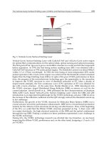
Fig. 1. Molecular -stacking along the monoclinic a axis of BDTDA, a photograph of a thin
film on ITO, and the molecular packing in the bc plane for this material
Anomalous Transient Photocurrent
555
2.1 Characteristics of BDTDA thin films
2.1.1 Film structures
BDTDA is a disjoint diradical. Molecular orbitals for the two unpaired electrons are
localised to separate five-membered rings, and exchange interactions between the two
radical centres are very small. Its crystal structure consists of a face-to-face BDTDA dimer,
indicating that intermolecular interaction is stronger than intradimer interaction. These
dimers show -stacking along the monoclinic a axis. Packing of dimeric stacks produces a
herringbone-like motif with electrostatic S
+
…N
-
contacts, in which all the molecular planes
of BDTDA are parallel to the bc plane. It is notable that BDTDA films consist of alternating
1-dimensional -stacking with molecular planes parallel to the substrates, as shown in Fig. 1
(Iwasaki et al., 2009; Kanai et al., 2009). Therefore, -stacking can bridge the distance
between bottom and top electrodes, which aids photoconduction between the electrodes.
Fig. 2. Bonding and antibonding supramolecular orbitals of radical dimer.
2.1.2 Imbalance of carrier transport in BDTDA films
Considering that two -radical BDTDA molecules exhibit face-to-face overlap, a bonding
supramolecular orbital and an antibonding supramolecular orbital are developed (Fig. 2). The
population of the bonding supramolecular orbital is concentrated at the centre of the dimer,
while that of the antibonding supramolecular orbital spreads outside along the R—R axis.
Since these radical dimers create stacking chains with - interactions, the antibonding
supramolecular orbitals are expected to form a wide band through a large interdimer overlap;
population of the lowest unoccupied molecular orbital (LUMO) spreads towards the outside
of the dimer. By contrast, the highest occupied molecular orbital (HOMO) forms a narrow
band. Therefore, a significant imbalance of carrier transport can be expected, specifically high
photoconductivity by the electron migration in the wide LUMO band and poor hole mobility
in the narrow HOMO band. In addition, the valence bond image (Iwasaki et al., 2009) suggests
that the photoexcited state includes a character of charge transfer, namely, R:R → R
+
R
-
, where
R is a radical. In other words, electrons will be directly promoted from one molecule to another
by photons, which can be regarded as a precursor stage of charge separation. These
characteristics are promising for developing photoactivities.
2.1.3 Space charge limited current in BDTDA films
To characterise the diradical film, photocells with a structure of ITO/BDTDA (300 nm) /Al
were prepared (Fig. 3) and current-voltage (J-V) characteristics were recorded. BDTDA was
Optoelectronics – Devices and Applications
556
prepared as described in a previous report (Bryan et al., 1996), and was thermally
evaporated onto ITO glasses. As a top electrode, Al was also thermally evaporated onto the
thin films. The effective area of this photocell was approximately 0.02 cm
2
. The sample was
then fixed into a cryostat with a pressure below 1 Pa. During measurement, the Al electrode
was grounded, and bias polarity was defined as plus when a positive bias voltage was
applied to ITO.
Fig. 3. Schematic views and an energy diagram of BDTDA photocells.
J-V characteristics were investigated using a picoammeter/voltage source under dark
conditions and the bias voltage was scanned from -3 V to 3V. As shown in Fig. 4(a), the J-V
curve exhibits a rectification behaviour, and rectification rate is approximately 10
2
at 2 V. This
behaviour is reasonable, as the work functions of the two electrodes are different, and non-
injecting (see energy diagram of electrodes and BDTDA in the inset of Fig. 3). The applied bias
V was corrected (van Duren et al., 2003) to compensate for the built-in voltage (V
bi
≈ 0.4 V) that
arises from work function difference between the two electrodes. Voltage drop across the
series resistance of BDTDA devices was ignored, as its value was negligibly small.
Figure 4(b) exhibits the log (J)-log (V) plots for the data in Fig. 4(a). This curve consists of
two regions with a crossover point at ~0.8 V, below which the J-V curve demonstrates
Shockley behaviour that is ascribed to the injection limited current. At higher voltages (V >
0.8 V), the J-V curve shows a linear dependence, and its slope can be estimated as ~4.9. This
value indicates that space charge limited current dominates the curve, though the
dependence does not satisfy Child’s law (J V
2
) (Coropceanu et al., 2007; Karl, 2003). This is
a bulk limited current ascribed to a trap-controlled space charge limited current or a space
charge limited current with a field dependence of carrier mobility (Blom et al., 1997; Sharma,
1995). Therefore, space charges are easily generated in this thin film devices, mainly due to
significant imbalance of carrier transport and relatively large thickness (300 nm).
Fig. 4. J-V characteristics of a BDTDA photocell under a dark condition; (a) linear plot of J
versus V; (b) log (J)-log(V) plot for the data in (a).
Anomalous Transient Photocurrent
557
2.2 Photoresponses of BDTDA films
To measure the photocurrent of the photocells, a monochromated light, and green laser (532
nm) that can produce a stronger illumination, were employed as light source to irradiate the
samples. To match the absorption band of BDTDA thin films, light with a wavelength of 560
nm was chosen for weak illumination to the transparent ITO electrode. We adopted lock-in
techniques or an AC method (Ito et al., 2008) for normalised photocurrent-action spectra.
Fig. 5. (a) Absorption spectrum of BDTDA thin film; the inset shows the whole data within
the range of 1.4-4.5 eV; (b) photocurrent-action spectra
2.2.1 Steady-state photocurrent of BDTDA films
To determine the optical properties of BDTDA thin films for photocurrent measurements,
absorption spectrum of the BDTDA thin film (100 nm) on a quartz substrate within the range
of 1.5-3.0 eV was recorded, as shown in Fig. 5(a). The inset shows data in the whole range of
1.2-4.5 eV. It is notable that there is a broad band around 2.1 eV that covers the whole visible
range. The molecular orbital calculations indicate that this broad band is a complex of various
electronic transitions, including intramolecular-, intradimer-, and interdimer transitions,
allowed in the dimeric structure of this disjoint diradical. Subsequently, we examined the
photoresponse of ITO/BDTDA (300 nm)/Al sandwich-type photocells.
Figure 5(b) shows the plots of photocurrent versus the photon energy (photocurrent-action
spectra) measured by a lock-in technique with bias voltages V
bias
= -3, -1 and 0 V.
Photocurrent is obtained in the whole range of visible light (1.8-3.0 eV), while it shows a
quick decrease below 2.2 eV. This decrease is possibly caused by the fact that absorptions
below this energy are due to intramolecular excitations. The wide-range response, shown in
Fig. 5(b), is advantageous for practical application as photodetectors.
Figure 6 is the photocurrent induced by green laser light illuminating from the ITO side with a
small reverse bias voltage V
bias
of -3V. Upon illumination, conductivity is enhanced with an
on/off gain of 1.810
2
under an excitation light intensity of 1.59 mW/cm
2
. The corresponding
photoresponsivity (R
res
) was calculated to be approximately 3.5 mA/W based on the relation
R
res
= (I
ph
)/IA, where A is the effective device area; I
ph
and I are the photocurrent and the
incident light intensity, respectively. The on/off ratio increases with the light intensity, and its
maximum value observed in our experiments is approximately 10
3
. Meanwhile, the
photoresponsivity demonstrates an inverse behaviour, and changes from 10
-1
to 10
-4
A/W,
which is comparable to that of the most advanced organic polymer photodetectors for visible
region (Hamilton & Kanicki, 2004; Narayan & Singh, 1999; O'Brien et al., 2006; Xu et al., 2004).
Optoelectronics – Devices and Applications
558
Fig. 6. On/off switching properties of the BDTDA photocell.
It is notable that the ITO/BDTDA/Al cells produce a photocurrent even at V
bias
= 0 V, due to
the potential difference of the electrodes, specifically ITO (4.8 eV) and Al (4.3 eV). This
photovoltaic behaviour is consistent with the energy scheme in Fig. 3 taken by UPS/IPES
measurements (Iwasaki et al., 2009). It is possible that the charge separation character in the
photoexcited state, namely R+R-, contributes to this photovoltaic behaviour.
2.2.2 Anomalous transient photocurrent of BDTDA films
Figure 7(a) shows the photoresponses of an ITO/BDTDA/Al photocell with a bias voltage
of 0 V. Upon illumination, a large anomalous transient photocurrent followed by a steady-
state photocurrent was observed. Upon removal of illumination, a negative anomalous
transient photocurrent was detected. Both the anomalous transient photocurrent and
steady-state photocurrent increase with increases in light intensity. Figure 7(b) demonstrates
the short circuit photoresponses under a reverse bias voltage of -2 V. Note that the
anomalous transient photocurrent can be dramatically suppressed by applying a bias
voltage. In particular, the negative current is nearly eliminated, while the steady-state
current is increased. It is notable that anomalous transient photocurrent values under the
zero bias can be comparable to those of the steady-state photocurrent under a bias voltage
V. Positive anomalous transient photocurrent with weak excitation light intensity (≤ 0.57
μW/cm
2
) decreases exponentially with time, and decay time of the positive anomalous
transient photocurrent shows light-intensity dependence. As shown in Fig. 7(a), a stronger
illumination causes faster decay. Meanwhile, for the light intensity of > 0.57 μW/cm
2
,
positive anomalous transient photocurrent cannot fit well with a single exponential
simulation. This indicates that anomalous transient photocurrent is a superposed signal
with different mechanisms.
Quantum efficiencies for steady-state photocurrent and anomalous transient photocurrent
were calculated by neglecting reflection losses at the device surfaces. Figure 8(a) shows the
intenal quantum efficiency (Pettersson et al., 2001) versus photon energy plots for the peak
values of the positive (red curve) and negative anomalous transient photocurrent (blue
curve) and for steady-state photocurrent under monochromatic illumination with weak
intensity from a halogen lamp. Intenal quantum efficiency values for the positive and
negative anomalous transient photocurrent show increases with an increase in photon
energy, and their values are considerably higher than that of the steady-state photocurrent
(black curve). It is notable that the transient intenal quantum efficiency for the positive
Anomalous Transient Photocurrent
559
anomalous transient photocurrent reaches an extremely high value of 65% at the photon
energy of 2.8 eV, and its root mean square value is estimated to be ~30%; intenal quantum
efficiency values of steady-state photocurrent are ~6%, corresponding to an external
quantum efficiency of ~2%.
Fig. 7. Photoresponses of a BDTDA photocell with an illumination of 560 nm; (a)
photoresponses under different light intensities with a zero bias voltage; (b) photoresponses
under different light intensities with a bias voltage of -2 V.
To explore the recombination processes and mechanisms for anomalous transient
photocurrent, we examined the light intensity dependence of the positive anomalous
transient photocurrent and steady-state photocurrent. The results are shown in Fig. 8(b),
where both axes are in a logarithmic scale. Both anomalous transient photocurrent and
steady-state photocurrent obey a power law: J I
, with = 0.93 for the former or = 0.28
for the latter. The former value suggests that monomolecular or geminate recombination
(Binet et al., 1996) plays a role in the process. The latter value suggests that the steady state
suffers from higher order recombination processes, such as Auger (Wagner & Mandelis,
1996) and quadrimolecular recombinations (Marumoto et al., 2004). Considering that the
value is close to 0.25, quadrimolecular recombinations are more likely; adjacent
photogenerated R
+
R
-
pairs may interact with each other and recombine simultaneously.
Fig. 8. (a) Intenal quantum efficiency values of the anomalous transient photocurrent and
steady-state photocurrent for a BDTDA photocell; (b) light intensity dependence of the
positive anomalous transient photocurrent (red points) and the steady-state photocurrent
(blue points) induced by the green laser.
Optoelectronics – Devices and Applications
560
3. Mechanisms of anomalous photocurrent in BDTDA
Due to imbalance of carrier transports and the energy scheme of photocells, the junction at
the Al/BDTDA interface plays the dominant role for the transient photoresponse (Hu et al.,
2010a) if the BDTDA film is fully depleted. On the contrary, ITO/BDTDA with a larger
barrier plays a main role if the film is not depleted. The junction acts as an active region
(dark pink region in Fig. 9), which makes a different contribution to the anomalous transient
photocurrent compared with the bulk region as blocking region (shallow pink region). The
thick film can be treated as a double-layer system with widths of d
a
and d
b
(Hu et al., 2010b).
Due to the large thickness and an imbalance of carrier transport, space charges are
accumulated in the active layer. The built-in electric field will be changed, which may lead
to the generation of polarisation current in the film.
Fig. 9. A schematic view of BDTDA photocells.
3.1 Total current in a double-layer model
Theoretic analyses were performed to explore the mechanisms. To simplify the related
theoretic analyses, electric fields in both regions are regarded as uniform and thus the
BDTDA films can be separated into a double-layer film. Moreover, the thickness of both
layers is assumed to be constant.
3.1.1 Theoretic analyses for a double-layer model
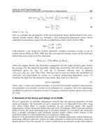
Based on the total current equation (Guru & Hiziroğlu, 2004), the current density j through
the double layers is written as follows:
a
00a0a0a
b
bbb b a
dE t dE t
jEt Et
dt dt
, (1)
where σ
b0
, σ
b
, ε
b,
and E
b
(t) pertain to dark conductivity, photoconductivity, relative dielectric
constant, and the time t dependence of the uniform electric field, respectively, in the bulk
blocking region. Meanwhile, σ
a0
, σ
a
, ε
a
, and E
a
(t) express the corresponding quantities in the
active junction region. The constant ε
0
denotes the dielectric constant of free space. The first
terms in both sides of Eq. (1) are conduction current, while the second terms are
displacement current. All parameters for conductivity are assumed to be time independent
and dark conductivities were ignored. Taking the bias voltage (V = E
b
d
b
+ E
a
d
a
) and the
boundary condition ε
b
E
b
(0)=ε
a
E
a
(0) into account, we can resolve Eq. (1), and the time
dependence of E
b
, E
a
and j can be written as:
/t
aaa
b
ba ab ba ab ba ab
V
Et Ve
dd dddd
, (2a)
Anomalous Transient Photocurrent
561
/t
bbb
a
ba ab ba ab ba ab
V
Et Ve
dd dddd
, (2b)
2
/
2
ab ba ba
t
ba
ba ab
ba ab b a a b
ddV
jV e
dd
dd d d
, (3)
where
0 ba ab
ba ab
dd
dd
. (4)
As shown in Eq. (4), the physics of decay time
τ relates to the extraction speed for the free
carriers by electrodes and dielectric property/polarisation in the films. Subsequently, we
can estimate the total collected charges at time
t in the active side electrode, which is given
by the following:
00
() () ()
tt
Qt A
j
tdt itdt
, (5)
where i(t) is the discharging current in the external circuit. We take into account that the
voltage drop across load resistor R is equal to that across the photocell, particularly the
following:
00
()
()
tt
Aj t dt i t dt
itR
C
, (6)
where C is the capacitance of the photocell. Since the initial current i(0) = 0, Eq. (6) can be
resolved and the external discharging current i(t) (i.e., anomalous transient photocurrent) is
expressed as follows:
0
() (1 )
tt t
RC RC
S
it e e S e
RC
, (7)
where
2
0
0
2
ab ba ba
ba ab b a a b
ddV
ddd d
,
ba
ba ab
V
dd
3.1.2 Simplified analyses for BDTDA photocells
In general, photogenerated excitons in organic materials can be dissociated only at donor-
acceptor interfaces, or by a strong local electric field (Nicholson & Castro, 2010). If the film
thickness is considerably larger tthan exciton diffusion length and carrier drift length, the
excitons and carriers far from the electrodes cannot contribute to the photocurrent. In other
words, the photoconductivity σ
a
, which is proportional to carrier mobility μ and density n in
the junction (active region), is considerably larger than that in the bulk region, as well as the
Optoelectronics – Devices and Applications
562
dark conductivity. Therefore, other conductivities (σ
b0
, σ
b
, and σ
a0
) can be ignored. Eqs. (2)
and (7) can therefore be expressed as follows:
/
1
t
a
b
bbaabb
V
Et Ve
dd d d
, (8a)
/t
b
a
ba ab
Et Ve
dd
, (8b)
tt
RC
S
it e e
RC
(9)
with
2
0 ba
ba ab b
dV
ddd
(10)
and
0 ba ab
ba
dd
d
. 11)
Obviously, photogenerated carriers in the junction region that can be collected by electrodes
will be exhausted if photoconductivity of the blocking region is extremely small. The space
charge will be accumulated in the film and thus the electric field can be changed, as shown
in Eq. (9). This naturally leads to a polarisation current. Two mechanisms, including
τ and
RC time constant, are responsible for the decay of the anomalous transient photocurrent.
The derivative calculation was performed for Eq. (9), and a rise time
τ
R
can be obtained. In
particular, after a time
ln
R
RC RCI
t
RCI
, (12)
with κ = τI = ε
0
(d
b
ε
a
+d
a
ε
b
)/d
b
eαμ, the largest current density J
m
can be achieved, which is
expressed as follows:
1
RC
RC
m
RC RC
J
RC
. (13)
Since σ
a
=eαIμ, where α is quantum efficiency and αI means carrier density with a light
intensity of I, and e means the elementary charge, the decay time τ can be written as follows:
0 ba ab
b
dd
ed I
, (14)
which suggests a relationship of τ I
-1
. This relation fits the experimental data well. We
consider the situation of a weak illumination, which will lead to a large τ. If τ >> RC, the
discharging current density in Eq. (9) will be
Anomalous Transient Photocurrent
563
t
m
JJe
, (15)
with a maxima J(t) value J
m
2
a
m
ba b a
dVe I
JI
dd
. (16)
Equation (15) suggests that the anomalous transient photocurrent exhibits exponential decay
under weak irradiation and/or with a very small RC time constant in the circuit, which fits
well with the experimental behaviour in Fig. 7(a). It is notable that
2
mb
J
in Eq. (16),
indicating the effects from the dielectric constant of the bulk region. On the contrary,
stronger illumination triggers a smaller
τ, which is related to the dielectric constants of the
materials and photoconductivity in the junction region. If
τ << RC, the time constant in the
circuits will dominate the decay, and shows resistance dependence as well as an exponential
relationship.
3.2 Discussions
Both Eqs. (7) and (9) indicate that the anomalous transient photocurrent is a superposed
signal with two mechanisms, namely, electron extraction from the junction region, and
discharging process in the external circuit with a time constant of
RC. It is clear that the
thickness of our BDTDA films (300 nm) is excessively large, exceeding the exciton diffusion
length and carrier drift length. Upon illumination, photogenerated electrons near the
cathode are extracted as conduction current, while electrons on the other side cannot move
across the thick film to compensate. This induces the transient conduction current.
The capacitance and dielectric constant in the equations involve polarization mainly in the
bulk region triggered by photogenerated space charges in the films. The dielectric property
of BDTDA strongly influences the anomalous transient photocurrent. Based on theoretic
analyses, it is natural that the anomalous behaviour is universal for the thin films with large
polarity, poor mobility and relatively large thickness. Though the carriers in organic
materials cannot withstand a long trip due to various means of dissipation, including traps
and recombination, displacement or a polarisation current can generate a large anomalous
transient photocurrent without experiencing a long trip. Fast generation of this photocurrent
is possible because the photoinduced polarisation current allows localised charges to
oscillate around their equilibrium states. This is promising for high-speed organic
photodetectors.
Fig. 10. A schematic display of an anode/ blocking layer /active layer/cathode photosensor.
4. Metal/insulator/semiconductor/metal type photocells
Based on the double-layer model, we developed a device to confirm the theoretic analyses in
Section 3. A transparent thick organic insulator layer as a blocking layer was adopted to
Optoelectronics – Devices and Applications
564
substitute the bulk region in BDTDA photocells, and an organic semiconductor thin layer as
an active layer was chosen to substitute the junction region. Figure 10 demonstrates the
photocell with a structure of metal/organic insulator/organic semiconductor/metal, which
may be utilised for light detection as well. The thickness of the semiconductor layer is
targeted around 20 nm, which is equivalent to the carrier drift length. The organic double
layers between the metals induce an imbalance of carrier transports; in particular, only one
type of carrier can be collected by the electrodes. These will facilitate accumulation of the
other type of carriers as space charges at the interface of the blocking layer and active layer.
In this structure, the dielectric property of the insulator layer will strongly influence the
signals.
Fig. 11. Chemical structures of PVDF and ZnPc:C
60
donor-acceptor systems.
4.1 Photoresponses of ITO/PVDF/ZnPc:C
60
/Al
To check the photoresponse of this kind of photocell, an equivalent metal/blocking
layer/semiconductor layer/metal photocell was fabricated with ITO and Al electrodes. A
well-known transparent polymer, polyvinylidene fluoride (PVDF, 8 wt% in dimethyl
formamide), was adopted for the blocking layer and spin-coated onto a hot ITO glass slide
(100 ºC). Thickness was estimated to be ~1 µm by cross-sectional SEM images. At the top of
the blocking layer, a 30-nm active layer with a high charge-separation efficiency was
prepared with zinc phthalocyanine (ZnPc) and fullerene (C
60
) (molar ratio: 1:1, see Fig. 11
for their molecular structures) by co-deposition. Subsequently, the Al cathode was thermally
evaporated onto the blend film. Photocurrent measurements were conducted under an
illumination from a green laser (532 nm) controlled by a multifunction synthesiser.
Photoresponses across a load resistor of 10
5
Ω were recorded on an oscilloscope.
Fig. 12. (a) Photoresponses of an ITO/PVDF/ZnPc:C
60
/Al photocell under an illumination
of different intensities; (b) a comparison between the absorption spectra of the blend films
(blue curve) and photocurrent-action spectra of the photocell (red curve).
4.1.1 Photoresponses
Figure 12 shows the photoresponses with various light intensities. Upon laser illumination,
a large anomalous transient photocurrent similar to that in the BDTDA photocells is
Anomalous Transient Photocurrent
565
observed, and a negative anomalous transient photocurrent appears just after the
illumination. Both the positive and negative anomalous transient photocurrent increase with
increases in light intensity, and a faster decay can be obtained under a stronger illumination,
which fits the expectation of Eq. (12). Absorption spectra of the blend films and
photocurrent-action spectra (Fig. 12(b)) were collected for comparison. The peaks in these
spectra are in agreement, indicating that the active layer does play a primary role in the
production of this anomalous transient photocurrent. It is notable that no signals were
obtained in the ITO/PVDF/Al structure, suggesting that only the active layer was the
sensitive component. In addition, the relationship between anomalous transient
photocurrent and weak light intensity was observed to exhibit linearity.
Fig. 13. (a) Photoresponses of an ITO/PVDF (1 µm)/ZnPc:C
60
(30 nm)/Al photocell with a
light modulation of 1 kHz (31.8 mW/cm
2
). (b) Frequency dependence of the photoresponses.
We examined the reproducibility of the anomalous transient photocurrent as well.
Continuous current oscillation induced by frequency modulation is stably observed without
degeneration (Fig. 13(a)). Evidently, the effective current will be increased as modulation
frequency increases, as more current peaks can be generated in a fixed time period. It is
notable that the values of the anomalous transient photocurrent peaks increase with
increases in modulation frequency, and saturation is subsequently achieved after a certain
modulation frequency, as shown in Fig. 13(b).
Fig. 14. (a) Simulations for the positive anomalous transient photocurrent based on (a) Eq.
(7) and (b) Eq. (12) at 100 Hz.
4.1.2 Theoretic analyses for the transient photocurrent
We performed theoretic simulations for the anomalous transient photocurrent from the
metal/blocking layer/semiconductor layer/metal photocells based on Eqs. (7) and (12), as
Optoelectronics – Devices and Applications
566
shown in Fig. 14. The blue triangles in Fig. 14(a) show the time dependence of the current
density of positive anomalous transient photocurrent obtained under an illumination of 31.8
mW/cm
2
. The solid red curve in this figure shows the theoretical simulations from Eq. (7).
The
RC time constant was extracted from the simulation to be 6.8×10
-5
s, which is
considerably close to the experimental value (4.2 ×10
-5
s, experimentally determined for the
present circuit by an LCR meter at 100 Hz).
τ was estimated to be ~1.6×10
-4
s, during which
1-(1/e) of the photogenerated carriers that can be extracted will be collected by electrodes.
The blue squares in Fig. 14(b) depict the dependence of the rise time
τ
R
on light intensity.
This behaviour is reproduced by Eq. (12) (solid curve) as well.
The RC time constant and τ
are estimated to be 8.3×10
-5
s and 1.4×10
-4
s under an illumination of 31.8 mW/cm
2
,
respectively. Both simulated values from Eqs. (7) and (12) are in approximate agreement
with each other, suggesting that the established double-layer model is reasonable for the
explanation of anomalous transient photocurrent.
Fig. 15. Impulse response of the ITO/PVDF/ZnPc:C
60
/Al photocell under a zero bias
voltage; the inset is a magnified version of the recovery process.
4.1.3 Impulse response
To evaluate the lifetime of anomalous transient photocurrent, an impulse response was
examined with a nanosecond laser beam (600 nm) from an optical parametric oscillator
pumped by a Nd:YAG laser (10 Hz; pulse width: ~6 ns; power: ~1.08 µJ/pulse). A digital
oscilloscope and a dc 300-MHz amplifier were used to collect voltage response with an
input resistance of 50 Ω. A photocell with a structure of ITO/polystyrene (1 μm)/ZnPc:C
60
(20 nm)/Al was prepared for comparison with the ITO/PVDF (1 μm)/ZnPc:C
60
(20 nm)/Al
photocells. The fabrication method for the polystyrene blocking layer was the same as that
for PVDF.
Figure 15 shows the impulse response of the photocell with a PVDF blocking layer, which
consists of rise, decay, and recovery processes. This behaviour is similar to that of the
pyroelectric detectors with slower rise, decay, and recovery times (Odon, 2005; Polla
et al.,
1991), though their mechanisms are quite different. The
RC constant in this circuit was
estimated to be ~5 ns. Rise and decay time of the PVDF photocell can be observed as ~15
and 100 ns, respectively. Both the rise and decay times show an
RC constant dependence;
they increase along with increases in the
RC constant (not shown). However, the recovery
time exhibits a long time scale of ~2.5 µs (see inset of Fig. 15) and is independent of the
RC
constant.
Anomalous Transient Photocurrent
567
Fig. 16. Dielectric constant dependence of the anomalous transient photocurrent under an
illumination (532 nm) of 160 mW/cm
2
; (a), (b) and (c) show the short-circuit anomalous
transient photocurrent in the metal/blocking layer/semiconductor layer/metal photosensor
with PVDF, polystyrene, and vacuum gap as blocking layers, respectively.
Faster response can be achieved by decreasing the dielectric constant ε of blocking layer. For
example, substitution of the PVDF layer (ε ≈ 7-13) (Kerbow & Sperati, 1999) by polystyrene
(ε ≈ 2.6) (Cullen & Yu, 1971) brings about a considerably faster rise (~5 ns) and decay (~8 ns)
times at 0 V, but recover time remains to be ~1 µs. Slow recovery time could be ascribed to
an energy barrier between the donor-acceptor and/or semiconductor-metal interfaces.
Considering that the polarisation current is proportional to the variation rate of
E
b
triggered
by the photogenerated space charges, a faster generation of space charges by a sharper light
pulse can bring about a larger anomalous transient photocurrent, even when only a small
number of space charges are generated. Therefore, device speed is mainly determined by the
rise and decay time, even though the system does not completely recover.
4.1.4 Dielectric influences
We examined the relation between the dielectric constant ε
b
of the blocking layer and the
quantum efficiency of anomalous transient photocurrent. Photocells with three different
blocking layers (1 µm), namely, with vacuum gap (
ε = 1), polystyrene, and PVDF were
prepared. Thickness of all the active layers is approximately 20 nm. Figure 16
demonstrates the short-circuit photoresponses of the three photocells against a strong
illumination (160 mW/cm
2
). The values of the anomalous transient photocurrent
dramatically increase with
ε
b
as predicted in Eq. (16). As such, we can control the transient
conversion efficiency by changing the
ε value of blocking layer. It is notable that the
positive anomalous transient photocurrent of the PVDF photocell is ~8×10
2
times larger
than that of the vacuum-gap photocell, though a rough estimation based on Eq. (16)
suggests a difference of two orders of magnitude. The internal quantum efficiency of
anomalous transient photocurrent in this PVDF cell under a weak illumination (0.2
µW/cm
2
; 560 nm) from a halogen lamp is calculated to be approximately 34% (root mean
square, rms). The photoresponsivity at 560 nm (0.2 µW/cm
2
) reaches 10 mA/W (rms)
Optoelectronics – Devices and Applications
568
even without applying a bias voltage, which is comparable to those of conventional
organic photodetectors operated by a bias voltage (Iwasaki et al., 2009; Narayan & Singh,
1999; O'Brien et al., 2006). It is believed that more charges stored in the PVDF photocell
with a larger
ε were released upon illumination, when compared with the polystyrene and
vaccum gap photocells.
Fig. 17. (a) Photoresponse of ITO/ ZnPc/polystyrene (1 µm)/Al photocells under a zero bias
voltage; (b) light intensity dependence of peak anomalous transient photocurrent value.
4.2 Photoconductivity dependence
Based on Eq. (14), decay time τ is inversely proportional to photoconductivity σ
a
= enμ,
where
n = αI is the photogenerated free carrier density. Therefore, larger carrier mobility
and density will induce faster decay and a larger signal if the
RC time constant in a circuit
is very small. To check this relationship, ZnPc (30 nm) as the active layer was utilised in
the metal/blocking layer/semiconductor layer/metal structure by thermal evaporation
with a speed of 1 Å/s. Polystyrene layer (1 µm) by spin coating was adopted as the
blocking layer. Two types of photocells with different structures for this material were
produced, namely, ITO/polystyrene/ZnPc/Al and ITO/ZnPc/polystyrene/Al. As
expected, the former does not exhibit signals since ZnPc is an excellent donor material.
The latter shows a signal (see Fig. 17) and only holes are collected by the ITO electrode,
which can be judged by the current direction. However, compared to those from the blend
film (or bulk-heterojunction) devices, the signal from ZnPc photocells is considerably
weaker due to a lower charge separation efficiency, which leads to a smaller carrier
density. We likewise examined the light intensity dependence of anomalous transient
photocurrent. As predicted in Section 3, intensity dependence of anomalous transient
photocurrent does exhibit linearity (Fig. 17(b)) under weak illumination with a
monomolecular or geminate recombination.
4.3 Discussions
Photoresponses from the metal/blocking layer/semiconductor layer/metal structure even
with a vacuum gap is promising, indicating potential for pulse light detection. As we
know, metal/semiconductor/metal type organic thin film device usually exhibits a large
dark current due to pin holes, which leads to a small photocurrent. The employment of a
blocking layer hampers the formation of pin holes and results in an extremely small dark
current. It is possible now to utilise ultrathin films only with the highest internal quantum
Anomalous Transient Photocurrent
569
efficiency for light detection. Compared with ideal metal/semiconductor/metal
photocells with the same thickness in which conduction photocurrent
J
ph
can be written as
follows:
ph
ba
Ve I
J
dd
, (17)
the metal/blocking layer/semiconductor layer/metal structure may exhibit a larger
anomalous transient photocurrent current if we select an appropriate blocking layer and
active layer with a small value of
d
b
/d
a
, and small dielectric constant ratio (ε
a
/ε
b
). These
can be judged from Eq. (16)
1
. Therefore, it is possible to release more stored charges in the
capacitor type photocells upon illumination in addition to the photogenerated free
carriers. Equation (14) likewise indicates a promising method for characterisation of
carrier transport. As we can see from this equation, the anomalous transient photocurrent
signal is related to carrier mobility and density. Therefore, mobility can be estimated if we
extract the decay time
τ from theoretic simulations, and obtain the photogenerated carrier
density by other methods, such as light-induced electron paramagnetic resonance
technique. In addition, we can utilise the metal/blocking layer/semiconductor
layer/metal structure to determine the carrier type in an organic semiconductor, as
described in Section 4.2.
5. Conclusion
In summary, we analysed the anomalous transient photocurrent in the BDTDA photocells
based on a double-layer model. Resuts indicate that the dielectric property of organic
materials will strongly influence the anomalous behaviour. For instance, a large dielectric
constant will induce a larger anomalous photocurrent. This was confirmed in equivalent
devices, such as ITO/PVDF or polystyrene/ZnPc:C
60
/Al, in which the PVDF and
polystyrene layer act as the bulk region, and the blend film acts as the junction region in the
BDTDA photocells. Both theoretic and experimental results fit well with each other,
suggesting that polarisation and fast extraction of photogenerated carriers in the blend film
play significant roles in this behaviour. The theoretic analyses likewise indicate that the
anomalous transient photocurrent may achieve a larger value if proper conditions are
satisfied, compared to the conventional metal/semiconductor/metal photocells with the
same total thickness. It is notable that the metal/blocking layer/semiconductor layer/metal
structure is immune from pin-hole effects which usually exist in ultrathin conventional
devices. Stored charges in the metal/blocking layer/semiconductor layer/metal capacitor
photocells can be released upon illumination, which is quite different from the conventional
principles for light detection or harvesting. These indicate potential optoelectronic
conversion for pulse light detection in various fields, including communications, remote
control, and image sensors. The obtained theory may also play a role in the characterisation
of carrier transport along the directions perpendicular to the electrodes in the
metal/blocking layer/semiconductor layer/metal photocells.
1
For comparison, Eq. (16) can be changed to the following:
22 22
/2
mababbaab
JVeI d d d d
.
Optoelectronics – Devices and Applications
570
6. Acknowledgments
The authors are indebted to Prof. Hiroshi Ito for his technical supports and constructive
suggestions. Also acknowledged are the research group members who contributed to this
work through useful discussions and provision of materials. This research was supported by
a Grant-in-Aid for Scientific Research from the Ministry of Education, Culture, Sports,
Science, and Technology (MEXT) and by CREST, JST. Dr. Hu also thanks the National
Natural Science Foundation of China (No. 11004172 and 10804098) and the Zhejiang
Provincial Natural Science Foundation of China (No. Y607472).
7. References
Andriesh, A. M. et al. (1983), Anomalous Transient Photocurrent in Disordered
Semiconductors - Theory and Experiment.
Solid State Communications, Vol. 48, No.
12, pp. 1041-1043, ISSN 0038-1098.
Binet, F.
et al. (1996), Mechanisms of recombination in GaN photodetectors. Applied Physics
Letters
, Vol. 69, No. 9, pp. 1202-1204, ISSN 0003-6951.
Blanchet, G. B.
et al. (2003), Large area, high resolution, dry printing of conducting polymers
for organic electronics.
Applied Physics Letters, Vol. 82, No. 3, pp. 463-465, ISSN
0003-6951.
Blom, P. W. M.
et al. (1997), Electric-field and temperature dependence of the hole mobility
in poly(p-phenylene vinylene).
Physical Review B, Vol. 55, No. 2, pp. R656-R659,
ISSN 0163-1829.
Bryan, C. D.
et al. (1996), Preparation and characterization of the disjoint diradical 4,4'-
bis(1,2,3,5-dithiadiazolyl) [S
2
N
2
C-CN
2
S
2
] and its iodine charge transfer salt [S
2
N
2
C-
CN
2
S
2
]. Journal of the American Chemical Society, Vol. 118, No. 2, pp. 330-338, ISSN
0002-7863.
Chakraborty, A. K. & Mallik, B. (2009), Photoinduced anomalous current changes in some
organometallic materials.
Current Applied Physics, Vol. 9, No. 5, pp. 1079-1087, ISSN
1567-1739.
Coropceanu, V.
et al. (2007), Charge transport in organic semiconductors. Chemical Reviews,
Vol. 107, No. 4, pp. 926-952, ISSN 0009-2665.
Cullen, A. L. & Yu, P. K. (1971), Accurate Measurement of Permittivity by Means of an Open
Resonator.
Proceedings of the Royal Society of London Series a-Mathematical and Physical
Sciences
, Vol. 325, No. 1563, pp. 493-509, ISSN 0950–1207
Forrest, S. R. & Thompson, M. E. (2007), Introduction: Organic electronics and
optoelectronics.
Chemical Reviews, Vol. 107, No. 4, pp. 923-925, ISSN 0009-
2665.
Gunes, S.
et al. (2007), Conjugated polymer-based organic solar cells. Chemical Reviews, Vol.
107, No. 4, pp. 1324-1338, ISSN 0009-2665.
Guru, B. S. & Hiziroğlu, H. R. (2004),
Electromagnetic Field Theory Fundamentals, Cambridge
Univ. Press, Cambridge. ISBN 0521830168.
Hamilton, M. C. & Kanicki, J. (2004), Organic polymer thin-film transistor photosensors.
Ieee
Journal of Selected Topics in Quantum Electronics
, Vol. 10, No. 4, pp. 840-848, ISSN
1077-260X.
Anomalous Transient Photocurrent
571
Hu, L. G. et al. (2010), Highly efficient alternating photocurrent from interactive organic-
radical dimers: A novel light-harvesting mechanism for optoelectronic conversion.
Chemical Physics Letters, Vol. 484, No. 4-6, pp. 177-180, ISSN 0009-2614.
Hu, L. G.
et al. (2010), Optoelectronic conversion by polarization current, triggered by space
charges at organic-based interfaces.
Applied Physics Letters, Vol. 96, No. 24, pp.
243303, ISSN 0003-6951.
Ito, H.
et al. (2008), Photocurrent of regioregular poly(3-alkylthiophene)/fullerene
composites in surface-type photocells.
Thin Solid Films, Vol. 516, No. 9, pp. 2743-
2746, ISSN 0040-6090.
Iwamoto, M. (1996), Transient current across insulating films with long-range movements of
charge carriers.
Journal of Applied Physics, Vol. 79, No. 10, pp. 7936-7943, ISSN 0021-
8979.
Iwasaki, A.
et al. (2009), Interactive Radical Dimers in Photoconductive Organic Thin Films.
Angewandte Chemie-International Edition, Vol. 48, No. 22, pp. 4022-4024, ISSN 1433-
7851.
Kao, K C. (2004),
Dielectric Phenomena in Solids Elsevier Academic Press, Amsterdam. ISBN
978-0-12-396561-5.
Karl, N. (2003), Charge carrier transport in organic semiconductors.
Synthetic Metals, Vol.
133, No. pp. 649-657, ISSN 0379-6779.
Kumar, A.
et al. (1987), Anomalous Decay of Photocurrent in Amorphous Thin-Films
of Ge
22
Se
78
. Physical Review B, Vol. 35, No. 11, pp. 5635-5638, ISSN 0163-
1829.
Marumoto, K.
et al. (2004), Quadrimolecular recombination kinetics of photogenerated
charge carriers in regioregular poly (3-alkylthiophene) / fullerene
composites.
Applied Physics Letters, Vol. 84, No. 8, pp. 1317-1319, ISSN 0003-
6951.
Mihailetchi, V. D.
et al. (2005), Space-charge limited photocurrent. Physical Review Letters,
Vol. 94, No. 12, pp. 126602, ISSN 0031-9007.
Narayan, K. S. & Singh, T. B. (1999), Nanocrystalline titanium dioxide-dispersed
semiconducting polymer photodetectors.
Applied Physics Letters, Vol. 74, No. 23, pp.
3456-3458, ISSN 0003-6951.
Nicholson, P. G. & Castro, F. A. (2010), Organic photovoltaics: principles and techniques for
nanometre scale characterization.
Nanotechnology, Vol. 21, No. 49, pp. 492001, ISSN
0957-4484.
O'Brien, G. A.
et al. (2006), A single polymer nanowire photodetector. Advanced Materials,
Vol. 18, No. 18, pp. 2379-2383, ISSN 0935-9648.
Odon, A. (2005), Voltage Response of Pyroelectric PVDF Detector to Pulse Source of
Optical Radiation.
Measurement Science Review, Vol. 5, No. pp. 55-58, ISSN 1335-
8871
Pandey, A. K.
et al. (2008), Size effect on organic optoelectronics devices: Example of
photovoltaic cell efficiency.
Physics Letters A, Vol. 372, No. 8, pp. 1333-1336, ISSN
0375-9601.
Optoelectronics – Devices and Applications
572
Pettersson, L. A. A. et al. (2001), Quantum efficiency of exciton-to-charge generation in
organic photovoltaic devices.
Journal of Applied Physics, Vol. 89, No. 10, pp. 5564-
5569, ISSN 0021-8979.
Polla, D. L.
et al. (1991), Surface-Micromachined Pbtio3 Pyroelectric Detectors. Applied
Physics Letters
, Vol. 59, No. 27, pp. 3539-3541, ISSN 0003-6951.
Saragi, T. P. I.
et al. (2007), Spiro compounds for organic optoelectronics. Chemical Reviews,
Vol. 107, No. 4, pp. 1011-1065, ISSN 0009-2665.
Sharma, G. D. (1995), Electrical and photoelectrical properties of Schottky barrier devices
using the chloro aluminium phthalocyanines.
Synthetic Metals, Vol. 74, No. 3, pp.
227-234, ISSN 0379-6779.
Slooff, L. H.
et al. (2007), Determining the internal quantum efficiency of highly efficient
polymer solar cells through optical modeling.
Applied Physics Letters, Vol. 90, No.
14, pp. 143506, ISSN 0003-6951.
Spanggaard, H. & Krebs, F. C. (2004), A brief history of the development of organic and
polymeric photovoltaics.
Solar Energy Materials and Solar Cells, Vol. 83, No. 2-3, pp.
125-146, ISSN 0927-0248.
Sugimura, A.
et al. (1989), Anomalous Photoinduced Current Transients in Nematic
Liquid-Crystals.
Physical Review Letters, Vol. 63, No. 5, pp. 555-557, ISSN 0031-
9007.
Tahira, K.&Kao, K. C. (1985), Anomalous Photocurrent Transient in Polyethylene.
Journal of
Physics D-Applied Physics
, Vol. 18, No. 11, pp. 2247-2259, ISSN 0022-3727.
van Duren, J. K. J.
et al. (2003), Injection-limited electron current in a methano-
fullerene.
Journal of Applied Physics, Vol. 94, No. 7, pp. 4477-4479, ISSN 0021-
8979.
Wagner, R. E. & Mandelis, A. (1996), Nonlinear photothermal modulated optical reflectance
and photocurrent phenomena in crystalline semiconductors .1. Theoretical.
Semiconductor Science and Technology, Vol. 11, No. 3, pp. 289-299, ISSN 0268-
1242.
Xu, Y. F.
et al. (2004), Photoresponsivity of polymer thin-film transistors based on
polyphenyleneethynylene derivative with improved hole injection.
Applied Physics
Letters
, Vol. 85, No. 18, pp. 4219-4221, ISSN 0003-6951.
Xue, J. G. (2010), Perspectives on Organic Photovoltaics.
Polymer Reviews, Vol. 50, No. 4, pp.
411-419, ISSN 1558-3724.
Part 6
Nanophotonics